


Abstract
The detailed electronic structure of a layered semiconductor 1T-TiS2 and its modification in Ni-intercalated Ni1/3TiS2 were studied beyond the full surface Brillouin zone by use of a momentum microscope and He-I light source on their in-situ cleaved surfaces. Clear dispersions associated with the electron Fermi surface (FS) pockets induced by the self-intercalated Ti in non-doped 1T-TiS2 around the M points, as well as the hole FS pocket induced by the surface Ni in Ni1/3TiS2 around the Γ point, were confirmed in the observed high-resolution EB(kx, ky) band cross sections. A bird's eye view of the two-dimensional band dispersions EB(kx, ky) clarified many complex band dispersions. The experimental results are compared with first-principles band calculations performed for the bulk as well as the one monolayer (ML)-TiS2 and surface-1ML-Ni1/3TiS2. The characteristic changes of the band dispersions near the Fermi level (EF) are ascribed to the contribution of the 3d states of the surface Ni atoms with the C3v symmetry in contrast to the 'D3d' symmetry of the intercalated Ni. The importance of experimental studies of band dispersions in the full Brillouin zone is demonstrated, showing the high potential of momentum microscopy.
Export citation and abstract BibTeX RIS

Content from this work may be used under the terms of the Creative Commons Attribution 3.0 licence. Any further distribution of this work must maintain attribution to the author(s) and the title of the work, journal citation and DOI.
1. Introduction
Studies of two-dimensional (2D) van der Waals materials have grown extensively to elucidate their extraordinary electronic properties [1–15], which are considered to be of high technological importance. Various 2D materials are attracting much interest because of the possible modification of their bulk-, surface-electronic, and magnetic properties by physical and/or chemical means by impurity doping, alloying, surface deposition/adsorption, or chemical reaction [1–16]. Even the surfaces of host 2D materials show characteristic electronic and magnetic properties due to the combination of spin–orbit coupling and time-reversal symmetry, for instance, in the case of topological insulators, a class of materials under hot debate today [1, 16]. Elucidation of the differences in the electronic structure among the bulk, monolayer, and surface are the key issues for which angle-resolved photoelectron spectroscopy (ARPES) is very powerful. Comprehensive maps of the electronic structure can often only be obtained with high measurement efficiency, as provided by current synchrotron radiation ARPES setups, before surface degradation modifies the surface electronic structure.
A transition-metal atom (M) intercalated 1T-TiS2, namely, MxTiS2, is known to show various unusual physical properties compared with non-doped 1T-TiS2 [13], depending upon the M species and its concentration. A paramagnetic-to-spin-glass or -to-ferromagnetic transition takes place for some M with increasing x [17]. In NixTiS2, hole pockets are suggested from the Hall measurement in contrast to MxTiS2 with Mn, Fe, and Co [13]. Therefore, detailed ARPES studies of these materials are strongly desired. Previous ARPES results [12, 13, 18, 19] were so far compared to band calculations based on self-consistent augmented plane wave (APW) [10, 11] or Hartree–Fock [20] methods. However, the influence of M intercalation on electronic and magnetic properties via mutual hybridization is not clarified yet. In the present experiment, we employed a recently developed momentum microscope [21] to measure comprehensive 2D momentum-resolved photoelectron maps for the layered semiconductor 1T-TiS2 [4–9] and Ni-intercalated Ni1/3TiS2 [10–15]. The novel measurement scheme of the momentum microscope collects all photoelectrons emitted into the complete solid angle above the sample and directly forms a 2D reciprocal space image on the detector. These momentum images represent constant energy cuts EB(kx, ky) through the initial-state band structure of the sample. The parallel imaging principle allows collection of each momentum image, covering more than the first-surface Brillouin zone (BZ) of the TiS2, within less than 3 min per binding energy (EB), even using a laboratory He gas discharge light source.
Our results reveal dramatic changes of the Fermi surface (FS) pockets, band dispersions, and broadenings in Ni1/3TiS2 compared to the non-intercalated host material. For a detailed understanding of the observed electronic properties, we compare the experimental results with advanced first-principles theoretical band calculations. As both experiment and theory cover large volumes in the E-k phase space, details of the electronic modification by Ni intercalation are revealed. Evidence is given that the electronic states near the Fermi level (EF) are dominated by the 3d states of the surface Ni atoms rather than by Ni atoms beneath the surface.
2. Experimental setup
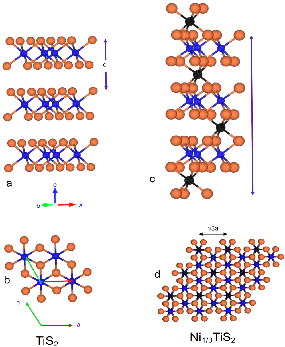
Here we studied 1T-TiS2 and Ni-intercalated Ni1/3TiS2. 1T-TiS2 has the CdI2-type structure, consisting of a sequence of Ti layers in the plane defined by the hexagonal lattice vectors a and b (angle 120°) and sandwiched between S layers (figures 1(a) and (b)) [6, 22], forming a S-Ti-S unit-layer (hereafter called monolayer TiS2 or 1ML-TiS2) [3]. Ti atoms are nearly octahedrally ('Oh') surrounded by six sulfur atoms (figures 1(a) and (b)). These TiS2 MLs are piled up along the c-axis via the van der Waals gaps.

Figure 1. Schematic atomic geometry of layered 1T-TiS2 (a), (b) and Ni1/3TiS2 (c), (d). The side view is shown in figures 1(a) and (c). Figures 1(b) and (d) show the look from the normal direction of the a-b plane. The dark orange and blue balls correspond to the S and Ti atoms, respectively. The black balls in figures 1(c) and (d) stand for the intercalant atoms M (in the present case, Ni). In the case of M1/3TiS2 in figures 1(c), the √3 a × √3 a triangular lattice is formed for M atoms in the three sites A, B, and C, as indicated in figure 1(c). The piling up along the surface perpendicular direction c is then presented as TATBTCTATBTC... and so on, if the 1ML-TiS2 is presented as T. The upper two atomic layers in figure 1(c) are out of the unit cell, indicated by the dark blue arrow.
Download figure:
Standard image High-resolution imageThe bulk BZ of 1T-TiS2 is schematically shown in figure 2(a) with the high symmetry points Γ, K, M in the central plane and A, H, L points in the upper- and lower-BZ boundary planes. The K', M', H', and L' points are 60° rotated from the K, M, H, and L points. Threefold symmetry is realized in this case. The blue curve in figure 2(b) shows the kz corresponding to the Fermi level (EF) under the excitation at hν = 21.2 eV for the experimentally evaluated inner potential V0 = 11 eV [13] and work function ϕ = 4.2 eV. A wide variety of atoms (M) can be intercalated into the van der Waals gaps. The intercalant atoms M in MxTiS2 (x < 1) occupy the 'D3d' interstitial sites (figures 1(c) and (d)) [11].

Figure 2. Schematic 3D BZ of 1T-TiS2 (a) and the kz corresponding to the EF for the excitation photon energy of 21.2 eV (blue line in (b)) on the assumption of well-defined kz. Although the Γ, M, K symmetry points are the naming for k⊥ = 0 (k⊥ ∼ 2.2 Å−1 in the present case), the same nomenclature is used to define the (kx, ky) points along the A-Γ-A, L-M-L, and H-K-H axes in this paper, since k⊥ in the present experiment is broadened and/or deviated from k⊥ = 0. The K' and M' points are 60° rotated from the K and M points. Bird's eye views of the 2D band dispersions with EB from EF to 1.825 eV in 1T-TiS2 and Ni1/3TiS2 are shown in (c) and (d). In figures (c) and (d), the view is at 73° from the sample surface normal.
Download figure:
Standard image High-resolution imageIn our photoemission experiments, we used a recently developed momentum microscope [21], consisting of photoelectron emission microscope (PEEM) optics, and an imaging hemispherical energy filter consisting of two hemispherical deflection analyzers in an S-type arrangement. After the exit of the energy filter, a 2D image detector records either the real-space PEEM image or the 2D momentum-resolved photoelectron distribution at constant energies, emitted from a 20 μm-diameter region of the sample surface. Due to the imaging properties of the objective lens of the momentum microscope optics, all photoelectrons emitted into the solid angle of 2π steradian above the sample surface are collected and focused into a momentum image with a linear kx and ky scale. The maximum parallel momentum accessible in the momentum image is only limited by the photoemission horizon. This is the maximum k// at which the excited photoelectron has enough energy to overcome the surface work function, given by k//max = 0.5123√Ek, with the kinetic energy Ek given in eV. In our experiments, using 21.2 eV photons, this results in a maximum radius of the momentum image of 2 Å−1 at EF.
The samples were cleaved in situ in an ultrahigh vacuum. The position of the sample with respect to the microscope was optimized by a hexapod sample stage with six degrees of freedom for the best condition for real−space as well as k−space imaging. The photoelectrons were excited by a He lamp (Specs UVS-300), where the unpolarized He-I line was focused onto the sample by a tubed ellipsoidal mirror. The cross section of the light beam at the sample position had a diameter of 1.2 mm. Differential pumping of the gas discharge lamp was employed to realize a vacuum at the sample in the order of 2 × 10⁻⁹ mbar.
Here, we briefly point out further advantages of the simultaneous 2D imaging of photoemission intensities in the wide 2D BZ by a momentum microscope. In conventional 2D ARPES, the sample is rotated and tilted to record the EB(kx, ky) for a wide range of wave vectors. In that case, the photon beam will not always hit a fixed spot on the sample. This leads to a dataset that reflects the electronic structure of different sample areas. In the case of a momentum microscope, the photon beam is fixed on the sample. In addition, the surface-parallel momentum components kx and ky are directly obtained with high accuracy rather than being converted from angular coordinates. The relative intensity of the photoemission at different (kx,ky) is uniquely compared. The parallelized, high-efficiency 2D detection scheme prevents any need for sampling one of the momentum axes with a lower density of data points. Therefore the possibility to overlook any tiny ARPES features is very low.
The resolution of this instrument is experimentally confirmed to be ΔE ≤ 12 meV and Δk ≤ 0.005 Å−1. A detailed discussion about the instrumental resolution is given in reference [21]. The present measurement is performed with Δkx and Δky ∼0.02 Å−1, as verified by the sharp cutoff at the photoemission horizon, and the energy resolution is set to ΔE ∼30 meV. Better resolution values do not provide additional information for the present sample. The rather moderate resolution setting allows us to record complete 3D datasets that cover a large EB range of 5.5 eV and a k// range of ±2 Å−1 within a total measurement time of only 8 h, using a laboratory light source. The 3D datasets were collected with EB steps of 25 meV, consisting of 221 constant-energy (kx, ky) momentum distribution maps. Degradation of the sample was checked by comparison of the (kx, ky) images at EF before and after the measurements and was found to be negligible.
3. Experimental results
A bird's eye views (or 3D view) of the measured 2D band dispersions are shown for EB from EF to 1.825 eV in figures 2(c) and (d), respectively. 2D band dispersions of the valence bands (VBs) are clearly visible, and the electronic states crossing EF are recognized. The stronger and wider FSs are seen in Ni1/3TiS2 compared with 1T-TiS2. The shift of the VB structures toward larger EB in Ni1/3TiS2 is also clearly observed in these results. Anisotropies in the dispersions of the FS pocket bands and deeper VBs are distinctly revealed. In the region with larger  the emergence of the VBs in the next BZ are recognized, as seen in figures 2(c). Band dispersions along any kx,y directions can be immediately derived from the colossal amount of the experimental dataset. Typical band dispersions of 1T-TiS2 are shown in figure 3(a) along the high-symmetry M-Γ-K directions. The intensity at EF near the M point is really weak relative to the strong intensity in the VB for EB ≳ 0.8 eV. There is no FS contour near Γ. With increasing EB from the VB top (VBT), at least three bands are observed for EB = 1.2–2.0 eV. In the EB region between 1.8–2.3 eV is additionally recognized a rather broad band ranging in 0 ± 0.2 Å−1.
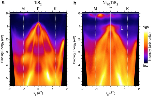
Figure 3. Band dispersions along M-Γ-K in 1T-TiS2 (figure 3(a)) and Ni1/3TiS2 ((b)). Please note that the value of kz in the experiment is deviated from the exact kz(Γ-K-M), as indicated in figure 2(b).
Download figure:
Standard image High-resolution imageCorresponding results for Ni1/3TiS2 are shown in figure 3(b). A much stronger intensity compared to 1T-TiS2 is recognized at EF near the M points. The non-flat extension of the near-EF states with finite dispersion along the M-Γ direction is clear. It is also confirmed that a hole FS with a clear dispersion is induced near Γ, where the increase in the diameter of the hole FS pocket with EB is revealed (more clearly seen later in figures 7(a)–(c)). In contrast to the rather sharp VBT in 1T-TiS2 near ∼0.8 eV, a much less dispersive lampshade band (L) is located near EB = 0.8–0.9 eV in Ni1/3TiS2. Since characteristic features of these typical band dispersions are desirable to be immediately compared with the theoretical band calculations described in section 4, comparison of detailed features in 2D EB(kx, ky) between experimental and theoretical results will be given in section 5.
4. Theoretical approach
First, we have determined the structural properties of these materials by the vdW-DF2 functional [23, 24] to take into account the van der Waals interaction. The calculated bulk lattice constants for TiS2 are a = 3.40 Å and c = 5.98 Å, and these values are found not to change much (less than 1%) in the Ni1/3TiS2, in contrast to the experimental values of a = 3.407 Å and c = 5.695 Å [25]. The expansion of the lattice is predicted to be negligibly small. We have used these calculated structural parameters in the following calculations.
We have performed first-principles calculations to clarify the nature of the electronic structure in 1T-TiS2 and Ni1/3TiS2, based on the density functional theory [26, 27] using the Vienna ab initio simulation package (vasp) [28, 29]. In our calculations for electronic structures, the exchange-correlation energy has been estimated in the Heyd–Scuseria–Ernzerhof (HSE) functional [30–32]. The HSE functional is a class of hybrid functionals mixing a part of exact exchange energy with the remaining part from the generalized gradient approximation (GGA). Only the short-range part of the exact exchange energy  is mixed in the HSE functional. We have adopted the mixing ratio to be 20% in this study. Then our applied HSE functional is explicitly written as the following:

where EGGA and  depict the total energy and the short-range part of the exchange energy of the GGA, respectively. We have used the projected augmented wave (PAW) method to expand the valence and core electron density. It is confirmed that the cutoff energy of 400 eV and the 6 × 6 × 1 k-point sampling in the hexagonal BZ of the √3 × √3 monolayer structure, or the equivalent sampling densities in other structures, are enough to assure the accuracy of 50 meV in the total energy and in the bandgaps.
In figure 4(a), we show the calculated band structure for the bulk 1T-TiS2. We see that the general features of the results correspond qualitatively to the experimental results. The VBT is located at the Γ point, and the conduction band minimum (CBM) is at the M point. The band dispersion of the highest occupied VB along the M-Γ direction spans an energy width of 2.0 eV, which is a bit larger than the experimental result. The calculation predicts a semiconducting behavior with a smaller energy gap of 0.4 eV compared to the experimentally evaluated value of ∼0.53 eV. The second highest VB, predicted to be rather flat around the Γ point, is predicted at EB ∼0.7 eV. However, this band is not observed in the experiment in the predicted EB region. The VB consists of hybridized d-orbitals of Ti atoms and p-orbitals of S atoms, and the conduction bands (CBs) are dominated by the d-orbitals of the Ti atoms.

Figure 4. Band dispersions along the M-Γ-K directions derived by HSE calculation for bulk 1T-TiS2 (a) and Ni1/3TiS2 (b). Corresponding results are also shown for 1ML-TiS2 (c) and surface-1ML-Ni1/3TiS2 (d). The bands are plotted with a constant Δk step. Therefore the intensity becomes higher when bands overlap or the broadening is decreased. If scattering and hybridization are negligible, each spot of the band should have the same intensity.
Download figure:
Standard image High-resolution imageFigure 4(b) shows the results of the HSE calculations for bulk Ni1/3TiS2, where we adopted a √3 × √3 super-cell to reproduce the intercalated system. The obtained bands are unfolded to the primitive BZ [33, 34] to facilitate a comparison with the results of 1T-TiS2. We note the absence of a clear bandgap in figure 4(b), and that the overall lifetime of the quasi-particle is shorter than in the non-doped case, as indicated by the lower intensity of the individual bands. We attribute the reduction of the quasi-particle lifetime dominantly to inelastic scattering of host electrons at intercalant atoms. This mechanism is explicitly taken into account by our theoretical model. In contrast, electron–electron scattering has been neglected in the calculation, treating the electron system by a mean-field approach. One flat and three dispersive bands are predicted along the Γ-M direction within ∼2.0 eV from EF. No hole FS pocket is predicted around the Γ point, in a strong contrast to the experimental results (figure 3(b)). The presence of a bandgap between the hole FS and the next VB at the Γ point clearly observed in the experiment is not predicted in the calculations.
In the calculated PDOS for the bulk Ni1/3TiS2 in figure 5(a), the most striking features are the location of the pronounced d-orbitals introduced by the Ni atoms, which are rather partially concentrated in energy regions around EB ∼ 1.8 eV and 0.5 eV. The components of CBs and VBs are not so much different from the non-doped 1T-TiS2 case (not shown), except for the energy range from 2.2 to 0 eV dominated by the Ni 3d states. Ni atoms are located not exactly at but close to the D3d sites ('D3d') surrounded by six sulfur atoms in the bulk. The crystal field causes the d-electrons of the Ni atom to be split into three irreducible representations of the group, i.e., Eg,A1g, and Eu located around EB ∼1.8, 1.2, and 0.5 eV, respectively, as recognized in figure 5(a).

Figure 5. The calculated density of states projected onto atomic orbitals (partial density of states: PDOS) derived by the same HSE calculation for bulk Ni1/3TiS2 (a) and surface-1ML- Ni1/3TiS2 (b).
Download figure:
Standard image High-resolution imageAs just stated above, the HSE calculations for the bulk Ni1/3TiS2 fail to explain the observed experimental results. After extensive efforts, we have found that we have to include the surface effect in the calculation model to well reproduce the experimental results in Ni1/3TiS2, because in this experiment the probing depth of the photoelectrons with the electron kinetic energies in the range of ∼17–12 eV is rather short, as < 5 Å [35].
Figure 4(c) shows the calculated band structure for 1ML-TiS2. One can recognize that the VBT is located at the Γ point, and the CBM at the M point is much closer to EF compared with the bulk band calculation. The flat band predicted to be near EB ∼ 0.7 eV in the bulk band calculation is now predicted near EB ∼ 2 eV.
Figure 4(d) shows the calculated band structure for the 'surface-1ML- Ni1/3TiS2,' defined as half of the intercalated Ni atoms left on the cleaved side of 1ML-TiS2 and no Ni atoms on the other side of 1ML-TiS2. We have here adopted a 2√3 × 2√3 super-cell method and unfolded the calculated band structure to the primitive cell BZ. The most striking feature is the hole FS pocket predicted at the Γ point and a clear gap existing below it. One can trace the hole FS dispersing down to EB = 0.4 eV. The next VBT is located at Γ with EB ∼ 1.2 eV.
Figure 5(b) shows the calculated PDOS for the surface-1ML- Ni1/3TiS2. It is clearly seen that the d-orbitals of Ni are concentrated just below EF within the range of 1.2 eV and split by the crystal field with C3v symmetry. Except for this region, the VB consists of hybridized eg-orbitals of Ti atoms and p-orbitals of S atoms, and the CBs are dominated by the t2g-orbitals of Ti. Thus, the main contribution to the FS comes from the d-orbitals of the surface Ni atoms.
5. Discussion
Since the band cross sections EB(kx,ky) are measured with high accuracy of Δkx and Δky by use of the momentum microscope, detailed comparison with the first-principles theoretical band calculations is feasible. The comparison for 1T-TiS2 (Ni1/3TiS2) between experimental and theoretical results is given in figure 6 (figure 7). The bottom right figure in figure 6 shows the primitive cell BZ at kz = 0, where the light incidence azimuthal angle is ϕ = 30° and its polar angle is θ = 70° from the surface normal. In the case of undoped 1T-TiS2, one notes that EF is in the bandgap, while it crosses the CB in the experiment due to the Ti self-intercalation. Therefore, we need to shift EF in the calculation for 1ML-TiS2 by 0.1 eV to be consistent with the experimental result. (The theoretically predicted band cross section at EB = −0.1 eV is shown in figure 6(f)). The degree of self-intercalation is, however, very small [6]. The theoretical results in figures 6(g)–(i) resemble those in figures 6(b), (d), and (e), judging from the distribution of the weak intensity regions. In addition, one can remember that the branching behavior of the relatively sharp VBT, which is experimentally observed in figure 3(a) near EB ∼1.1 eV around k║ ∼ 0.4 Å−1, is well reproduced in the theoretical calculation given in figure 4(c). The observed broad band in EB ∼ 1.8–2.3 eV and k// ∼0 ± 0.2 Å−1 in figure 3(a) corresponds well to the top of the M-shaped band predicted in figure 4(c). The dispersions along the M-Γ-K directions and the regions without bands shown in figure 3(a) and the representative features of the EB(kx,ky) slices in the wide EB range in experimental results in figure 6 are qualitatively well reproduced theoretically for 1ML- TiS2, even though the calculated results at kz = 0 show sixfold symmetry. The possible reason for this is discussed later, since it is seen in both cases of 1ML-TiS2 and surface-1ML- Ni1/3TiS2.

Figure 6. Experimentally obtained typical 2D band cross sections EB(kx, ky) for 1T-TiS2 chosen from 221 slices are given in (a)–(e). Since the intensity near EF is rather weak, the intensity at EF is magnified four times. Typical band cross sections derived from the same HSE calculation are given in (f)–(i). The lower right figure shows the primitive cell BZ at kz = 0. The azimuthal angle of the incident light is at ϕ = 30°. The polar incidence angle is θ = 70° from the surface normal direction.
Download figure:
Standard image High-resolution image
Figure 7. Experimentally obtained 2D band cross sections EB(kx, ky) for Ni1/3TiS2 chosen from 221 slices are given in (a)–(g). Since the intensity near EF is rather weak, the intensity at EF is magnified three times, and the intensities at 0.1 and 0.25 eV are both magnified two times. (h) shows the primitive cell and 2√3 × 2√3 super-cell BZs at kz = 0, where the M point in the super-cell is indicated by Msc. Typical band cross sections derived from the HSE calculation are given in (i)–(l). The azimuthal and polar angles of incidence are the same as in figure 6.
Download figure:
Standard image High-resolution image
The typical band cross sections for Ni1/3TiS2 are given in figures 7(a)–(g). Much stronger FS intensity at the M points as well as the finite intensity at the Γ point compared with 1T-TiS2 are clearly seen in figure 7(a). The stronger intensity in the electron FS pockets must be due to the modification of the CB by Ni intercalation, resulting in the rising of EF and more filling electrons in the electron FS pockets. The presence of the hole FS is recognized when one compares the results of figures 7(a)–(c). In addition, a circular shaded-off band (C) passing through the inner part of the electron FSs around the Msc points is recognized in figures 7(a) and (b). As one can recognize in figure 7(i), the present theory can successfully predict the finite intensity in the region of Msc corresponding to the ring-like structure (C) observed in the experiment for Ni1/3TiS2 (figures 7(a) and (b)). If no Ni atoms are lost on the cleaved surface and perfectly √3 × √3 periodicity remains, the Msc point in the super-cell BZ and the M point in the primitive cell are equivalent and have comparable intensity. When only half of the Ni atoms are left on the surface in the form of a 2√3 × 2√3 super-cell, scattering of the Ti 3d states is increased, and the intensity at the Msc points is decreased. Then, weak intensity is predicted near the Msc and Msc' points. The randomness of the surface Ni atoms induced by cleavage further blurs the signal in these regions. Thus, the inner circle C in the experimental results (figures 7(a) and (b)) is ascribed to the long-distance 'partial' ordering of the surface Ni atoms. The experimental results in figures 7(d), (e), and (g) are also qualitatively well reproduced by the results in figures 7(j), (k), and (l). The opening of a gap between the hole FS around the Γ point and the next prominent VB (L) seen in figure 3(b) is well predicted in figure 4(d). The observed experimental features near EF are fully explained by this surface-1ML-Ni1/3TiS2 model.
The partial density of states (PDOS) of the surface-1ML-Ni1/3TiS2 (figure 5(b)) clearly demonstrates that the d-electron spectrum of the surface Ni atom is much different from that of Ni atoms sandwiched by two TiS2 MLs (figure 5(a)); namely, the energy distribution width is much narrower, and the center of gravity of the band is shifted by roughly 0.5 eV toward EF. The surface Ni atoms are located at C3v sites surrounded by three sulfur atoms, which means the crystal field is very different from the case of intercalated Ni atoms at 'D3d' interstitial sites. In fact, we have found that the potential at the topmost C3v position is 0.6 eV higher than that at the corresponding sites in the sandwiched position, according to the GGA calculation [36]. Furthermore, we have found that the effective potential at the second Ni layer is almost the same as in the bulk, differing by less than 0.1 eV. Thus, we have found that the surface Ni atoms make a great contribution to the present ARPES results, making the model of the surface-1ML-Ni1/3TiS2 the most suitable for interpretation of the experimental results. If the Ni atoms on the surface are ordered, the hybridization-induced band width may become smaller because of the reduced number of nearest S atoms. However, their widths are rather broad near the Γ point due to the randomness of the location of Ni atoms on the surface.
The prominent global intensity asymmetry between the lower left and upper right regions at EB larger than 1.6 eV in figures 6 and 7 is induced by the off-normal light incidence direction (θ ∼ 70° and ϕ = 30°), namely, an effect known as the linear dichroism in angular dependence of photoelectrons [37]. Even for the unpolarized excitation light, the p-polarized component induces more photoelectron excitation than the s-polarization component due to the metal optics at the sample surface. Then the characteristic feature for the p-polarized light dominates in the intensity distribution: symmetric with respect to the light incidence plane (defined by the light incidence direction and the surface normal) and the intensity change along the ϕ = 30° M-Γ-M' direction, as recognized in figures 6(b)–(e) as well as figures 7(c)–(g).
Although the theoretically predicted intensity in figures 6 and 7 becomes sixfold symmetric for kz = 0 due to the time-reversal symmetry, the FS intensity off the Γ-K-M planes becomes different between kx,y and −kx,y. The quasi-threefold symmetry of the M point FSs in Ni1/3TiS2 is explicable by taking the kz ≠ kz(Γ-K-M) effects into account. The results in TiS2 also show noticeable deviation from the sixfold symmetry, reflecting the deviation from kz = kz(Γ-K-M). In the near future, hν dependence of the ARPES measurement should be made by momentum microscopy to check this kz-dependent effect in the normal incidence configuration.
6. Conclusion
In contrast to many preceding ARPES studies, dispersions of the two kinds of FS pockets are clearly revealed in the present experiments for Ni1/3TiS2, demonstrating that the states are not due to the localized defects or impurities distributed randomly in the crystal. The bird's eye views of the 2D band dispersions helped us to identify subtle modifications of the band structure of 1T-TiS2 upon Ni intercalation.
Although the surface electronic structure of layered semiconductors has so far been thought to be rather similar to their bulk electronic structure, it is demonstrated here that it can be much different when the surface environment is different from that in the bulk: namely, the sites of the Ni atoms on surface-1ML-Ni1/3TiS2 have C3v symmetry, in contrast to the 'D3d' symmetry of the bulk intercalated Ni atoms. This results in a much different crystal field splitting of the Ni 3d states on the cleaved surface and in the bulk.
It is recently known that surface electronic structures are dramatically modified by surface doping in topological insulators [38]. Such a specific surface electronic structure in various materials must fully be understood to develop devices utilizing the peculiar electronic properties on some surfaces of layered systems. Since band cross sections at any EBs as well as band dispersions in any kx,y planes are very easily and reliably derived from the colossal EB(kx, ky) dataset, momentum microscopy is an invaluable tool for the detailed understanding of the exotic electronic properties of many solids under hot debate today. Even by using a laboratory He lamp, momentum microscopy can be as powerful as current synchrotron radiation-based ARPES setups. In addition, momentum microscopy can easily be extended to the use of synchrotron radiation, namely, soft and hard x-rays, and facilitate complete three-dimensional EB(kx, ky, kz) band mapping of bulk electronic structures.
Acknowledgments
The authors are much obliged to A Krasyuk and M Schmidt for technical advice and comments. SS thanks H Negishi and M Inoue for providing samples, attracting his interest into the 1T-TiS2-layered semiconductor and its transition-metal- intercalation system.