


Abstract
Semiconducting graphene nanoribbons (GNRs) are envisioned to play an important role in future electronics. This requires the GNRs to be placed on a surface where they may become strained. Theory predicts that axial strain, i.e. in-plane bending of the GNR, will cause a change in the band gap of the GNR. This may negatively affect device performance. Using the tip of a scanning tunneling microscope we controllably bent and buckled atomically well-defined narrow armchair GNR and subsequently probed the changes in the local density of states. These experiments show that the band gap of 7-ac-GNR is very robust to in-plane bending and out-of-plane buckling.
Export citation and abstract BibTeX RIS

Content from this work may be used under the terms of the Creative Commons Attribution 3.0 licence. Any further distribution of this work must maintain attribution to the author(s) and the title of the work, journal citation and DOI.
For graphene to reach its full potential in electronic applications, it is essential to introduce a band gap [1]. There exist various ways to do so, ranging from creating graphene nanostructures, to inducing strain [2–5]. In case of graphene nanoribbons (GNRs), the band gap depends on the width and termination of the ribbon. This makes GNRs promising structures for application in future electronics, especially if they are atomically well-defined. Sizeable band gaps are only obtained for armchair edge GNRs (ac-GNR) having a width on the order of 5–15 atoms[3–5]. When such an ac-GNR would be integrated into a (macroscopic) device it will almost certainly experience some form of strain. This raises the question how strain affects the electronic structure of ac-GNRs.
Thus far, the influence of axial strain and in-plane bending strain on the electronic structure of GNRs has only been addressed theoretically. Depending on the type of strain, changes in the band gap ranging from a few tens of meV to 1 eV have been predicted [6–9]. Experimental verification of these predictions are scarce, especially for in-plane bending and buckling. Recent advances in the preparation of GNRs allow for synthesis of atomically precise 7-ac-GNRs on Au(111) under UHV conditions [10]. The electronic structure of these ribbons is well characterized [11–13]. High-resolution direct/inverse photoemission spectroscopy gives a band gap of 2.4 ± 0.4 eV [13]. Scanning tunneling spectroscopy (STS) measurements find a comparable band gap (2.6 eV) [12, 13]. In a scanning tunneling microscope (STM) experiment the GNR could also be picked up to perform conductance measurements along its long axis [14]. In this experiment the conductance is observed to decrease when the GNR is lifted from the surface. This is ascribed to out-of-plane bending of the GNR.
Here, we study how in-plane bending of atomically well-defined ac-GNRs affects their electronic structure. The ribbons are bent using the tip of a STM. The changes in the electronic structure are subsequently probed using STS.
All experiments were performed in a low temperature STM/AFM (Omicron GmbH) kept at 4.5 K using a tuning fork in the Q-plus design as the force sensor (24.454 Hz, Q = 12.000, oscillation amplitude: ∼86 pm). 7-ac-GNR are grown by evaporating the precursor molecule 10, 10'-dibromo-9, 9'-bianthryl onto a clean Au(111) surface kept at 200 °C, as described previously [10]. Subsequent heating to 400 °C leads to the formation of atomically well-defined ac-GNRs. All STS spectra are recorded using a lock-in amplifier with the oscillator set to 293 Hz, 10/20 mV rms.
Figure 1(a) shows an atomically resolved AFM image of an ac-GNR measured with a metal terminated tip, overlaid with an atomic model. The measurement is performed in constant height mode. Above the edges of the ribbon, there is a large attractive interaction between tip and sample, as indicated by the large negative frequency shift. At these points the GNR might be lifted slightly from the surface due to the reactive metal tip. Note that chemically passivated tips (typically CO terminated) are required to avoid accidental pick up of small molecules [15]. The GNRs are just big enough to allow them to be imaged with metal tips.

Figure 1. (a) 7-ac-GNR overlaid with an atomically resolved AFM image. (b) STM image of 7-ac-GNR (V = 100 mV, I = 100 pA) with colored crosses indicating positions of STS spectra, scale bar 5 nm. Scale bar: 5 nm. (c) and (d) Experimental and calculated (TB) STS spectra on ac-GNR (25 monomer units).
Download figure:
Standard image High-resolution imageSTS spectra recorded at several positions over a GNR as indicated in figure 1(b) are shown in figure 2(c). The onset of the valence band around −0.8 V. The onset becomes less steep when STS spectra are recorded closer to the end of a ribbon. Tight Binding calculations (TB) performed on gas-phase ribbons predict that the states on ac-GNRs can be considered as monomer states modulated by a 1D particle-in-a-box envelope function. Since the intensity of this envelope function varies spatiality, a decrease in the local density of stated is expected towards the end of the GNR. STS spectra extracted from the TB calculations (figure 1(d)) are in good agreement with the experiment. Note that the broad in-gap resonance between −0.5 and 0 V is due to the Au surface state under the ribbon.
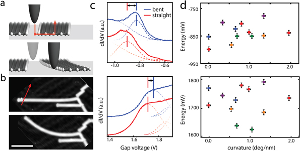
Figure 2. (a) Schematic of GNR bending: after the feedback loop is disconnected, the tip is moved towards the surface and the GNR is pushed by the tip. (b) Top, a straight GNR with the tip trajectory indicated. Bottom, after manipulation the GNR is at its maximum curvature of 2 deg/nm. Scale bar: 10 nm. (c) STS spectra of valence band (top) and conduction band (bottom) recorded for bent/straight ribbons. (d) Position of valence band (top) and conduction band (bottom) recorded on several ribbons (indicated by colors) with different curvatures.
Download figure:
Standard image High-resolution imageThe STM tip can be used for the manipulation of small molecules or atoms[16]. The same methodology can be used to bend GNRs. Briefly, in-plane bending of an ac-GNR is done by placing the tip next to the GNR, disconnecting the feedback loop, moving the tip a few Angstroms towards the surface, and moving the tip in the direction of the desired bend (figure 2(a)). After the manipulation, the feedback loop is reconnected and an image is obtained of the bent ac-GNR (figure 2(b)). We find that the maximum curvature that can be obtained for an ac-GNR using this procedure is 2 deg/nm. The critical curvature that a GNR can sustain depends on the corrugation of the interaction energy. Above a curvature of 2 deg/nm the lateral forces induced by bending are sufficient to cause relaxation to a less strained conformation. An example of the changes in the electronic structure of a GNR due to bending to a curvature of 2 deg/nm is shown in figure 2(c). For this ribbon, the valence band onset is shifted to lower bias by 59 ± 10 mV(figure 2(c), top), while the conduction band shifts to higher bias by 26 ± 10 mV (figure 2(c), bottom). Hence, the band gap changes by only 33 mV (1.3%). Figure 2(d) shows the position of the valence/conduction bands of several GNRs, plotted as a function of curvature. For in-plane bending of ac-GNRs up to curvatures of 2 deg/nm, there is no clear correlation between curvature and position of the conduction and valence bands. Part of the spread in the data may be related due to the fact that it is impossible to acquire spectra at exactly the same position before and after manipulation (combined with the uncertainty originating from the data fitting). In addition, (minor) tip changes due to the manipulation cannot be excluded and not all ribbons had an equal length. Nevertheless, in all cases we find that for curvatures up to 2 deg/nm the effect of bending on the band gap is small, on the order of a few percent.
Note that since both the valence and conduction band shift in the same direction, we can rule out that the shift of the bands is caused by a change in voltage distribution in the tunnel junction (caused by e.g. a change in the adsorption height of the GNR on the Au(111)). Also, a slight buckling (induced by bending) is deemed unlikely: buckling would result in one of the arm-chair edges being closer to the substrate, whereas the opposite edge is further away. This should lead to a shift in opposite directions on the two sides of the GNR. However, this is not observed experimentally. In addition, we did not observe differences in the apparent height along the short axis of the GNRs. Considering the above, we believe that the observed shift of the valence and conduction bands, as well as the small changes in the band gap are caused by the in-plane bending.
The electronic structure of distorted GNRs is governed by an effective axial strain that is a cumulative sum of contributions due to axial stretching, bending, and/or twisting [17]. In case of axial stretching, the distances between the atoms, and therefore the C–C interaction (i.e. the magnitude of the hopping integral in tight-binding calculations), should change significantly. This should result in large changes in band gap. In contrast, if strain causes bond angles to distort, the magnitude of the C–C interaction—and therefore the band gap—should not change much. Hence, we tentatively conclude that the strain induced by in plane bending is predominantly accommodated in distorted bond angles. This is consistent with the calculated ratio of the bond and angle stiffness [18, 19].
To investigate the mechanism of bending (pushing or pulling) as well as to bend ac-GNR beyond 2 deg/nm, an additional z-step (typically 8 Å with respect to a set point of V = 100 mV, I = 20 pA) towards the surface was made before reconnecting the feedback loop. This additional z-step reproducibly resulted in the deposition of a small cluster of atoms next to the ribbon (see figure 3(a)). We believe that the tip pushes the GNR since the cluster of atoms ends up on the side of the ribbon from which the tip came. This small cluster allows us to push the GNR beyond a curvature of 2 deg/nm (figure 3(a)-1/2). Above a curvature of 4 deg/nm ac-GNRs start to buckle. This buckling is seen in STM images as a large increase in apparent height at the buckling site. Upon removing the metal cluster using STM manipulation (typical parameters: constant height mode, with the tip brought closer to the surface by 3 Å w.r.t. a set point of V = 100 mV, I = 0.8 nA), the buckled GNR does not relax to a more straight conformation, indicating that it corresponds to a stable configuration (figure 3(a)-bottom left). The blue STS spectrum in figure 3(b) is recorded on a straight part of a buckled ac-GNR. For comparison, an STS spectrum acquired on the same ribbon before buckling, but with a different tip (due to deposition of a metal cluster) is also given (red). The spectrum acquired on the buckled ribbon shows the same features as a spectrum obtained on a straight GNR (valence band at −859 mV, onset of the Au(111) surface state at ∼−400 mV and the conduction band at 1757 mV) [12, 13]. Buckled GNRs can be returned to (nearly) straight configurations. STM images acquired after 'unbuckling' do not reveal any defects, demonstrating that the buckling is a non-destructive process (figures 3(a)–4).

Figure 3. (a) Bending of ac-GNRs beyond 2 deg/nm. Arrows indicate the direction of tip motion. Top left image: 2 manipulations steps to bend a GNR beyond 2deg/nm. After the second step, the tip is brought in contact with the surface to deposit a small cluster of atoms to prevent GNR relaxation. Top right: cluster is removed by lateral STM manipulation (typical parameters: constant height mode, with the tip brought closer to the surface by 3 Å w.r.t. a set point of V = 100 mV, I = 0.8 nA). Bottom left: the buckled GNRs can be straightened by lateral manipulation. Bottom right: STM image after straightening the buckled GNR. Scale bar: 2 nm. (b) STS spectra recorded on a nearly straight ribbon (red) and on a straight part of a buckled GNR (blue). The inset shows where the spectra where acquired.
Download figure:
Standard image High-resolution image
Figure 4. (a) STM image of an intact GNR (50 mV, 2 pA). (b) STM image (100 mV, 50 pA) of a buckled GNR after scanning the as-grown GNR multiple times at 3.7 V, 500 pA. (c) Constant height AFM image of the buckled ac-GNR shown in (b). (d) Height profiles of ac-GNR before and after buckling (dotted lines in (a) and (b). (e) STS spectra recorded on an ac-GNR before (blue) and after buckling (red, green) (see inset). The location where the spectra where taken are indicated in (a) and (b). Scale bars: 1 nm.
Download figure:
Standard image High-resolution image
Finally, we can use the STM tip to buckle the ac-GNR along the entire edge, resulting in a so-called partial-single walled nanotubes (p-SWNT) [20]. Figure 4(a) shows an intact ac-GNR. Figure 4(b) shows the same GNR after scanning several times at high bias (3.7 V). A single voltage pulse of this magnitude leads to breaking of a C–H bond and formation of a C–Au bond [13]. The ribbon appears narrower and the apparent height is decreased w.r.t. the as-grown ribbons (see figure 4(d), location of the line profiles indicated in 4(a) and (b)). A constant height AFM image of this ribbon (figure 4(c), acquired with a metal tip) has a loss of contrast near the edges, consistent with a buckled structure [21]. Additionally, the large areas of attraction, seen for the intact GNR (figure 1(a)), are no longer present. This suggests that the ribbon is more strongly coupled to the surface, in agreement with the narrower appearance and the lower apparent height. The above observations strongly suggest that (almost) all C–H bonds are broken and that multiple C–Au bonds are formed. Due to the mismatch of the GNR structure with the underlying Au lattice, the p-SWNT is not evenly buckled. Comparing STS spectra taken at a similar position before and after buckling reveals a large change in the position of both the conduction and valence bands (red and blue curves in figure 4(e)). These changes are consistent with an increased coupling to the surface. Spectra acquired at the zigzag edge of the p-SWNT (green spectrum in figure 4(d)) do not exhibit the end-state present for intact GNRs [13]. Interestingly, the onset of the valence band is observed at exactly the same position on the zigzag and ac-edge but the conduction band at the zigzag edge is located at higher bias. For defect-free ribbons the conduction band onset is observed at the same voltage on the zigzag and armchair edges [13].
To conclude, we have subjected atomically precise ac-GNR to several different types of STM manipulations. For in-plane bending of ac-GNRs up to curvatures of 2 deg/nm, there is no clear correlation between curvature and position of the conduction and valence bands. The changes in the band gap are on the order of a percent. A GNR can also be buckled, transforming it to a p-SWNT, by contacting the carbon atoms along the ac-edge to the Au substrate via tip induced bond formation. The buckled structure can be visualized using atomically resolved AFM. In this conformation the states of the ac-GNR broaden significantly due to increasing coupling to the surface.
We acknowledge discussions with Cristiane Morais Smith. This research was supported by NWO (Chemical Sciences, Veni-grant 722.011.007).