


Abstract
We report here on the presence of two different nonvolatile resistive switching mechanisms in Pt-Pr0.67Ca0.33MnO3-Pt sandwich structures based on pulsed electrical transport measurements. As a function of pulse length, amplitude and temperature, the devices show two different switching regimes. The first is positive switching (PS) where a high resistance state (HRS) evolves at positive bias at the top electrode in the voltage range of U ≈ 0.5–1.2 V and pulse lengths tp ≈ 10−7 s. In addition, we observe a cross over to negative switching (NS) for U > 1 V and tp ≈ 10−3 s. Here, the HRS evolves at negative bias applied at the top electrode. We present strong evidence that both switching mechanisms take place at the interface between Pr0.67Ca0.33MnO3 and the top electrode. Based on finite element simulations of the temperature evolution during the electrical pulses, we show that the onset of Joule heating is characteristic of the PS regime, whereas drastic temperature increases of several hundred Kelvin evolve during NS. Based on the observed different timescales, pulse amplitudes and temperature dependences of PS and NS, respectively, we suggest that two different switching mechanisms are involved: a fast, short range exchange of oxygen at the interface with the metallic electrode for PS and a slower, long range redistribution of oxygen in the entire PCMO film for the NS.
Export citation and abstract BibTeX RIS

Content from this work may be used under the terms of the Creative Commons Attribution 3.0 licence. Any further distribution of this work must maintain attribution to the author(s) and the title of the work, journal citation and DOI.
1. Introduction
A large variety of transition metal oxides embedded in metal electrodes exhibit nonvolatile resistance changes under external electric stimulation. This makes them possible candidates for resistive random access memory (R-RAM) applications [1, 2]. Pr1−xCaxMnO3 manganite thin films sandwiched by precious Pt electrodes exhibit both volatile and nonvolatile resistance changes (e.g. [3]). Such manganites belong to the class of strongly correlated electron systems. The electric conductivity in the p-doped Pr1−xCaxMnO3 is governed by the hopping transport of small polarons [4]. Volatile resistance reductions are observed in electric fields due to driven polaron states with enhanced conductivity, both in bulk single crystals [5] as well as in lateral thin films geometry [6].The small polaron mobility is thermally activated. Higher temperatures, also due to Joule heating, can therefore significantly reduce the resistance.
In cross plane geometry, higher amplitudes of electric stimulation can be easily achieved and induce remanent resistance changes. For Pr1−xCaxMnO3 the reversible switching between low resistance states (LRS) and high resistance states (HRS) is bipolar, i.e. after switching from a LRS to a HRS, one can only return to the LRS by applying an electric pulse with the opposite polarity. Depending on the amplitude of the excitation, intermediate states can also be reached, i.e. multi-level switching is possible [1].
We focus here on Pr0.67Ca0.33MnO3 (PCMO) sandwiched by two noble metal electrodes (Pt), where switching due to oxidation/reduction of the bulk electrode material (as observed e.g. for Al [7] and Ti [8] electrodes) should be very limited. This allows us to study processes which are located within the oxide films or at the interfaces between the oxide and the noble metal, respectively. There are models for resistive switching without altering the metallic electrode; Mott transitions [9, 10], Schottky barrier effects [11], polaron ordering [12] or electro-chemical effects related to the migration of oxygen/cation vacancies [13]. Although there is some consensus that at sufficiently large electric stimulation migration effects can be initiated in many oxides, the existence of a single universal switching mechanism and the role of electronic correlation effects remain elusive.
Like other oxide systems [14–17], Pt-PCMO-Pt exhibit two different bipolar switching regimes, depending on the applied electric stimulation amplitude [18]. They differ in switching polarity, and are therefore defined as positive and negative switching regimes, PS or NS, respectively, since positive or negative pulses are required to establish the HRS. In voltage cycling experiments the NS (PS) corresponds to a clockwise (counter-clockwise) remanent resistance change. In symmetric devices the appearance of NS and PS can be explained by a single switching mechanism which occurs at the two opposing interfaces at different stimulation amplitudes [15, 19]. In contrast, our devices are asymmetric. We show that the voltage drop mainly takes place at the top electrode interface and that also the resistive switching takes place only at the interface to the top electrode. The two observed switching regimes are attributed to two different switching mechanisms occurring in the device under electric stimulation at different time scales and voltage pulse amplitudes. Filamentary switching as reported in other oxides (e.g. [16]) seems to be rather unlikely due to the lack of initial forming steps or visible device modifications.
We present systematic measurements of the nonvolatile resistance change dependent on the duration and the amplitude of the applied excitation pulse at various temperatures. Our results indicate that the underlying processes of resistance change have different activation energies for the NS and PS regimes, respectively. Finite element simulations of the temperature evolution of the used devices during electric pulses show that significant Joule heating is especially present in the NS regime. Time scales, current ranges and the sign of the voltage for the NS regime are fully consistent with a Joule heating assisted long-range bulk oxygen migration process altering the oxygen vacancy distribution in the PCMO very close to the interface by exchanging vacancies with the bulk. In contrast, for the PS regime, the temperature increase due to Joule heating is less prominent. In addition, the shorter time scales, the switching polarity and the smaller current densities/voltages for PS switching are compatible with a short-range oxidation (e.g. electro-chemical) of the metallic electrode interface.
2. Methods
2.1. Device preparation
Our devices consist of Pr0.67Ca0.33MnO3 (PCMO) films sandwiched between Pt electrodes. The films are successively deposited by the ion beam sputtering technique on 10 × 10 mm MgO single crystal substrates. First, about 450 nm of Pt as the bottom electrode, followed by 300 nm of PCMO, are deposited at 1023 K under 1.4 · 10−4 mbar O2 and 1.0 · 10−4 mbar Xe (sputter gas) background pressure. All PCMO films reveal the orthorhombic crystal structure with dominating [001] orientation perpendicular to the substrate, but with different degrees of twining and different volume fractions (<10%) of (112) misorientations.
In order to confine the top electrode, a photo resist lacquer (Allresist, U-4040) with small holes is used as an insulator on the extended PCMO film. The holes with diameters of a few μm are created by a photolithography technique and provide the top electrode contacts on the PCMO after the final Pt layer is deposited on top of the stack (see schematic in figure 1(b)). The top electrode Pt layer is deposited at room temperature without oxygen partial pressure. A low deposition temperature is necessary because deposition at high temperatures would lead to a decomposition of the organic lacquer which remains on the sample. The lacquer also provides an insulating interlayer for the supply lines leading to the top electrodes on the film. Five different devices were used for this contribution. The devices are fabricated using the same procedure and showed only insignificant deviations in the relevant properties. The different top electrode diameters lead to different overall resistance. Therefore abbreviations with the electrode diameter will be used: A, C (both 5 μm) and B, D, E (4 μm).
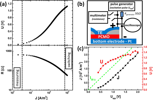
Figure 1. (a) Nonlinear dynamic applied voltage U and device resistance R as a function of 1 ms current pulses by Keithley 2430 current source. (b) Schematic view of the device geometry and the electric measurement setup with the pulse generator. (c) Calibration of the applied sample voltage and current density as a function of the applied voltage of the pulse generator. The green line shows the result of an ohmic sample resistance of R = 30 Ω for comparison. (300 K, device C, 5 μm).
Download figure:
Standard image High-resolution image2.2. Pulsed electric measurements setups
In the following, the excitation pulse is characterized by the resistance R, the current density J, the voltage drop U and the pulse duration tp. Scaling of the resistance with respect to device cross-section and thickness [3] implies a rather homogeneous current transport across the device. We therefore calculate J from the current and the full device cross section for comparison of differently sized samples. Nevertheless, the actual current-carrying cross section might be smaller i.e. J should be interpreted as an overall current density. Underlying device diameters are mentioned in the figure captions.
Figure 1(a) shows a typical U-J and R-J dependence, respectively. For small currents, the resistance is current independent. At higher current densities, a nonlinear regime evolves which is characteristic for polaronic transport. Nonvolatile resistive switching commonly occurs beyond J ≥ 108 A m−2. The excitation pulse can be either applied in voltage-controlled or current-controlled modes, respectively. Using a J-controlled pulse mode avoids a current runaway due to nonlinear R(U) behavior and thus does not require compliance limits. However, the occurrence of PS and NS switching is independent of the measurement mode. Therefore current and voltage amplitude are in general treated as pulse amplitude. The remanent resistance changes are probed after the excitation pulse at small probe pulses Uprobe in the ohmic regime. The resistances R+ and R− correspond to the probe resistance after positive and negative excitation pulses. The switching amplitude is defined as ΔR/R− = (R+−R−)/R−.
Two different measurements setups are used for the pulsed measurement of J-U curves and remanent resistance changes: cross plane electric transport properties at voltage or current pulses of duration tp = 1 ms (probe and excitation pulse) are obtained by using a Keithley 2430 current/voltage source. Uprobe was fixed at 0.08 V and the delay time between subsequent probe and excitation pulses was about 200 ms. For electric excitation on time scales down to 100 ns, a pulse generator (Agilent 81101A) was used (figure 1(b)) in combination with a Keithley 2000 multimeter. The generator and multimeter were electrically separated from the device by a relay box leading to a longer delay time of about 500 ms between excitation and probe of the remanent resistance. The multimeter measured the remanent resistance at Uprobe = 0.2 V for about 300 ms. The applied pulse trains used for both measurement setups are sketched in the insets of figures 2(a) and (b).
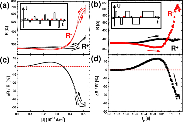
Figure 2. Remanent resistance after alternating pulses with (a) variable current amplitude/fixed pulse length (tp = 1 ms) and (b) pulses with variable pulse length/fixed amplitude (Uapp = 1.5 V). The insets show the corresponding pulse schemes with alternating excitation pulse polarity (open bars) and small voltage pulses (filled bars) used for measuring the remanent resistance at low voltages. R+ (black) and R−(red) represent the remanent resistances measured after the application of positive or negative of the excitation pulses, respectively. The arrows in (a) indicate the two branches obtained for increasing and decreasing pulse current amplitudes. In (b) only the branch for increasing pulse lengths is shown. The corresponding, normalized switching amplitude ΔR = R+−R− for (a) and (b) is presented in (c) and (d), respectively. ((a/c) device A, 5 μm, (b/d) device B, 4 μm.).
Download figure:
Standard image High-resolution imageFor the experiments involving the pulse generator, a calibration procedure is required to gain actual voltage drop U. Since the pulse generator has an internal resistance of 50 Ohm, it is configured such that the sample resistance is equal to the value of the internal resistance. Consequently, when setting the generator e.g. to Uapp = 1.5 V, a voltage of 2 Uapp = 3 V will be applied to the series circuit of sample and internal resistance which leads to a sample voltage of 1.5 V for a 50 Ohm sample. Since the sample resistance is voltage dependent, we have used an oscilloscope to measure the actual voltage drop for various Uapp (figure 1(c)). This calibration between U and Uapp was also applied to another sample (see caption of figure 7(a)).
3. Results
3.1. Dependence of switching amplitude on pulse amplitude and pulse length
Figure 2 demonstrates the remarkable similarity of the influences of the pulse current density and the pulse duration on the nonvolatile resistance changes. The actual development of the two resistance states R+ and R−after the application of a positive/negative pulse for a fixed tp = 1 ms and increasing J is plotted in figure 2(a). Figure 2(c) shows the corresponding switching amplitude ΔR/R− = (R+−R−)/R−. At small current densities no difference between R+ and R− is visible. A positive switching amplitude (R+ > R−) evolves above J ≈ 109 A m−2, i.e. the HR state corresponds to R+. The amplitude increases up to a maximum at about J ≈ 2.5 · 109 A m−2 and then decreases with increasing current density. At ≈ 3.5 · 109 A m−2 the switching amplitude vanishes, i.e. the resistance states R+ and R− are equal. Larger currents now exhibit R+ < R− and therefore negative switching amplitude (the HR state corresponds to R−) evolves, where the switching polarity is reversed. Note the good reversibility of the process: while successively reducing the pulse current density from its maximum value, the R+ and R− branches are very close to the R+ and R− branches for increasing J. Furthermore, at low currents, the initial resistance value of the cycle is approached, where R+ ≈ R−. Only the first cycling of the device (starting from virgin resistance state) causes some irreversible changes in R+ and R− (supplement S6). The initial resistance is typically about 3–4 times higher than the virgin resistance ([3], supplement S3).
It is worthwhile to note that, after a first initial sequence, further sequences with the same maximum pulse length or maximum current (voltage) are well reproducible. The switching amplitude ΔR is voltage/current dependent, but nearly independent of the actual R+ and R− (see supplement S6), most likely due to the strong nonlinearity of device resistance in the switching regime. Therefore the amplitude between R+ and R− is only current dependent i.e. R− decreases and R+ increases when J is decreased after Jmax. The final resistance after each cycle is the sum of all previous switching processes and is, remarkably, almost constant for switching sequences which are symmetric with respect to the increase and decrease of applied pulse amplitude/length.
The qualitative same R+/R− characteristics can be observed for alternating pulses with variable pulse length at fixed stimulation amplitude Uapp (figure 2(b)). For very small pulse lengths tp ≤ 10−6 s no switching is observed. With increasing tp positive switching also occurs (ΔR/R− (tp) > 0, see figure 2(d)) until a maximum is reached. For longer pulses, ΔR/R− (tp) is reduced again and shows a sign reversal at about tp = 5 · 10−2 s.
Figure 3(a) gives an overview of the combined effect of pulse length and pulse amplitude (here expressed by Uapp) on ΔR/R−. Since the negative switching has much larger switching amplitudes, the modulus was taken. Note that the curve at Uapp = 1.5 V (green line) is the same as in figure 2(d). The polarity change from PS to NS is now represented by a dip in |ΔR/R−| at a characteristic pulse length tp which shifts to longer pulse lengths for decreasing Uapp. For Uapp = 1.0 V, the PS to NS transition is shifted beyond the studied maximal pulse length of tp = 1 s. Therefore, no negative switching is observed. Also the onset of the positive switching shifts to increased pulse lengths with decreasing Uapp. The shortest visible time scale for switching of tp ≈ 10−6 s is given by the time constant of the RC circuit of the measurement setup and is thus not an intrinsic time scale of the device (see also figure 4).
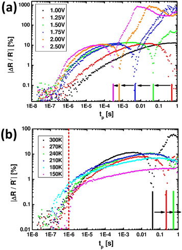
Figure 3. Modulus of switching amplitude of the same device as in figure 2(b) for different Uapp voltages at 300 K (a) and for different temperatures at fixed Uapp = 1.5 V (b). Note that a more pronounced shift of the initial PS onset to shorter tp with increasing temperature might be hidden in the transient regime below tp = 10−6 s (device B, 4 μm).
Download figure:
Standard image High-resolution image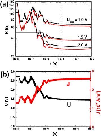
Figure 4. Time evolution of the device resistance R, sample voltage U and current density J during a 1 ms pulse measured by an oscilloscope. (a) R at different Uapp for positive (black) and negative (red) sign of the bias. (b) Voltage drop U and resulting current density J for the 1 ms pulse with Uapp = 2.0 V. The initial flat line at 2.7 V represents the limit of the oscilloscope (actually higher voltage, less current) before the initially high resistive sample dynamically reaches low resistance at about 1 μs (device C, 5 μm).
Download figure:
Standard image High-resolution imageFigure 3(b) shows the temperature dependence of |ΔR/R−|. A strong increase in the PS amplitude with increasing resistance is observed at lower temperatures, where the thermally activated polaronic transport (R(T) ∝ T exp(E/kT)) in PCMO leads to a strong increase in the resistance (see supplement S1). Remarkably, the switching amplitude ΔR/R− follows an almost universal curve at positive switching, i.e. the resistance difference ΔR(tp) = R+−R− scales with initial R(T). In contrast to the PS regime, both the onset as well as the magnitude of the NS switching amplitude is strongly temperature dependent: the transition to negative switching is successively shifted to longer pulse lengths and |ΔR/R−| drops with decreasing temperature. Below T = 240 K, the transition is even shifted to tp > 1 s outside the accessible measurement range of our study.
3.2. Temporal evolution of the stimulation pulse
In addition to the study of the remanent resistance change after the application of the stimulation pulse, we have conducted experiments to analyze the resistance evolution during a stimulation pulse. For such experiments based on the pulse generator, the nonlinear resistance behavior of the device in combination with the internal 50 Ohm resistance (in series) of the pulse generator has to be taken into account. It influences the time evolution of the applied voltage which is actually applied to a sample as a function of time and Uapp: the temporal evolution of the resistance, current density and voltage during a 1 ms pulse applied by the pulse generator are demonstrated in figure 4 for a typical sample. Figure 4(a) shows the time evolution of the dynamic device resistance during an excitation pulse of 1 ms with different values of Uapp. For one of the pulses (Uapp = +2 V), the corresponding voltage and current densities are plotted in figure 4(b).
At the beginning of the pulse (t < 10−8 s), the sample exhibits a greater resistance (ohmic resistance of this device is about 600 Ω) than the internal 50 Ohm resistance of the pulse generator and experiences almost the full voltage amplitude of 2 × Uapp (not visible in figure 4(b) due to limited measurement range). Since the device resistance is high, the current is low. In the regime 10−8 s ≤ t ≤ 10−7 s the device resistance has dropped well below the ohmic regime, but no voltage dependence is visible for the different applied Uapp. Between 10−7 s ≤ t ≤ 10−6 s this dependence becomes visible in our measurement setup. However, the resistance drop of the sample is overlaid by more or less reproducible oscillations on a time scale of the RC circuit (extended contacts on the device, bonds, cable, etc) for all times below 10−6 s. For t > 10−6 s, the device resistance is reduced to a value comparable to the internal 50 Ohm, leading to a decrease in the actual U with increasing current density J. A well-measurable dynamic resistance is therefore established above 10−6 s. This time scale is independent of the applied Uapp. Note that this transient regime for t < 10−6 s might suppress initial resistive switching at shorter pulse lengths (see also figure 2).
The J-U characteristic of devices commonly reveals a small asymmetry with respect to the current direction. It is therefore worthwhile to note that the slightly higher resistance at positive excitation pulses (figure 4(a)) is not related to the formation of the HRS in the PS regime. In general, small remanent resistance changes have only negligible influence on the dynamic, nonlinear polaron resistance, especially at higher voltages. The measureable difference between the HRS and LRS decreases with increasing Uprobe, as the dynamic resistance curves for both states approach each other at higher voltages (see [3]). Therefore small switching effects occurring in the PS regime are invisible in the dynamic resistance. However, the slight increase of the resistance during the pulse with –Uapp = 2.0 (red curve) indicates a crossover to negative switching (for further support, see supplemental material S2). This implies that during a 1 ms pulse the initial positive switching is followed by the negative switching in time. The observed switching amplitude seems to be a result of the overlay of an initial fast but saturating positive switching and a slower but more pronounced negative switching process. As a consequence it is important to note that the switching amplitude in figure 2(d) can be qualitatively interpreted as the actual development of the remanent resistance during a single, long pulse since the switching evolution during long pulse lengths contains the characteristics of shorter ones.
3.3. Temperature evolution during the electric pulses
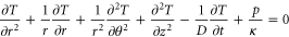
The time and space dependent temperature evolution due to Joule heating can dramatically influence the underlying mechanisms of the resistance change. The influence is therefore studied numerically [20] by finite element modeling using COMSOL Multiphysics®. We partition the total device into different areas, where the partial differential equation of heat conduction is solved in the time domain. These areas are (with thickness): the MgO substrate (1 mm), the bottom (600 nm) and top electrode (500 nm) made of Pt, the insulating layer (PMMA), the passive area of the PCMO layer below the PMMA resin and the electrically contacted area of the PCMO layer (300 nm) between the top and the bottom electrode. In good approximation to the experimental geometry, the device is axisymmetric (see figure 5(a)). The heat equation is therefore treated in cylinder coordinates:
including the thermal diffusivity D =  /(ρ cp) and the Joule heating volume power density p = R(T) J2 A/d. The values used for the local thermal conductivity
  specific heat cp and densitiy ρ are given in table 1. These three values are given at room temperature and approximated as temperature independent.
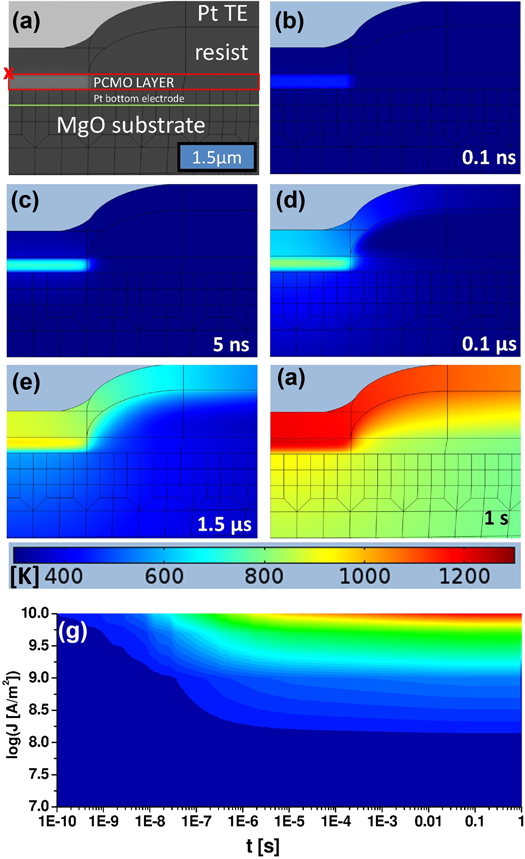
Figure 5. Simulated temperature evolution within the Pt-PCMO-Pt devices based on finite element simulations for J = 1010 A m−2 (see supplement S1 for details) (a) Scheme of simulated device, (b)–(f) spatial temperature distribution for different time steps. (g) Temperature evolution in time at different given current densities in the PCMO in the device center at the top electrode interface, see red cross in (a).
Download figure:
Standard image High-resolution imageTable 1. Parameters used for thermal finite element simulation.
| Parameter\material | PCMO | Pt | MgO | PMMA |
|---|---|---|---|---|
| Cp (J kg−1 K) | 480 [21] | 130 [22] | 873.6 | 1470 [23] |
| κ (W mK−1) | 1.58 [24] | 71.6 [22] | 56.975 | 0.2 [25] |
| ρ (kg m−3) | 5700 | 21450 | 3585 | 1200 |
Due to the dominating resistance contribution, the Joule heating (p-term) is exclusively induced in the electrically contacted PCMO layer between the top and the bottom electrodes, which represents the diameter (3 μm) of the device. The heat generated depends on the temperature dependent electric resistance R(T). This results in a drop in the Joule heating power during temperature increase. We apply a fit function R(T) = 77.86/T0.5 exp(1272.26/T) Ω to the experimentally measured data points (between 140 and 300 K) and extrapolate R(T) up to temperature T = 2000 K, where no experimental values are accessible (see figure S1(a) in supplement).
All outer boundaries are adiabatic (the top electrode on the surrounding PMMA is extended to 10 mm) except the substrate mount. Here, we consider an ideal thermal contact between the 1 mm thick substrate and the mount so that the ambient temperature is given as an isothermal boundary condition. Since PCMO is a poor thermal conductor and exhibits a relatively high electric resistance, a tremendous temperature increase is expected in short intervals. As a consequence both the time discretization and the spatial mesh discretization were chosen to be small. We apply time steps down to ts = 1 · 10−13 s and a finite element mesh with an element size of dm ≈ 2.5 · 10−8 m in the domain of the PCMO layer. The additional resistance drop due to the applied voltage is disregarded in this work. Thus we consider exclusively R(T) instead of R(T, U).
Figures 5(b)–(f) show the spatial distribution of the temperature evolution at J = 1010 A m−2 at different time steps. Clearly, the temperature increase at the bottom electrode is much smaller compared to the top electrode and also compared to the film center. In the stationary state close to a 1 s pulse duration, the highest temperatures evolve at the PCMO interface with the top electrode. This effect might become even more pronounced if a series resistance of the PCMO-top electrode interface was taken into account.
The simulated temperatures can be compared with the experimental observation of the melting of the top electrode material by performing switching experiments in a SEM (see figure S1(b) in supplementary material). We conclude from this calibration that the absolute temperatures are somewhat overestimated in the finite element calculations. This is due to disregarding the resistance drop by the applied voltage and the slight decrease in κ(T), reducing the actual generated power and increasing the heat conduction for a given current density. We observe that the timescale of about 10−6 s for the cross over between the rapid temperature increase and a moderate further increase due to the warming up of the bottom electrode and the substrate does not strongly depend on the current density (figure 5(g)). In the following, we define the regime of slowly increasing temperature with T ≈ (¾-1) Tend as the quasi-stationary state. We therefore expect that this timescale is not significantly affected by the approximations used. It is important to note that Joule heating at pulse amplitudes and time scales relevant for NS lead to temperatures up to a few hundred K in the device.
Another important result of the simulations is that the temperature increase in the stationary state is proportional to the heating power density P per unit area, i.e. ΔT = q U J = q P. This result is used for the simulations of the microscopic processes involved in PS and NS. We obtain q = 1.0 · 10−7 Km2 W−1 from experiments (see supplement figure S1(b)) which is below the qsim ≈ 1.6 · 10−7 Km2 W−1 obtained from the simulations after approaching the stationary state. It is plausible to assume a general calibration T ≈ 0.6 Tsim also qualitatively valid during the temporal temperature evolution as can be seen in figure 5(g).
3.4. Localization of resistance change in the device
In order to identify the interfaces which are involved in the resistance change, a third Pt-electrode ('center') was prepared as a reference close to the top and bottom electrodes by conventional lithography and focussed ion beam etching (figures 6(a) and (b)). The freestanding top electrode was contacted by a conductive micro-tip in an advanced SEM system, as described in more detail in [3]. After applying the excitation pulse between top and bottom electrodes, the remanent resistances were subsequently measured in two-point geometry (Keithley 2430, 1 ms pulses) for all three contact combinations by means of a relay box: between top and center, between bottom and center and between bottom and top electrodes (figure 6(a), pulse setup) with delay times of about 500 ms between all pulses.
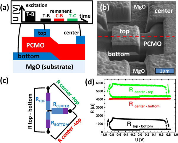
Figure 6. Determination of resistance change at the top and bottom electrodes, respectively, by using an additional third electrode ('center'). (a) Schematic cross section of device used and pulse configuration. (b) Tilted SEM—image of device (red dotted line represents the cross section in (a)). (c) Equivalent circuit for the resistance measurement. (d) Remanent resistance in NS mode between top and bottom (Uprobe = 0.08 V), center and bottom as well as center and top (Uprobe = 0.2 V, both) electrodes after applying pulse voltage between top and bottom (in voltage cycle measurement).
Download figure:
Standard image High-resolution image
Figure 7. (a) ΔR/R− (%) for different U and pulse length tp at 300 K for device B (4 μm). The pulse length is successively increased from tp = 10−6 s to 1 s and back (not shown) for six different Uapp as shown in figure 3(a). Positive switching (ΔR > 0) is marked by red color; negative switching (ΔR− < 0) by blue color. Zero switching amplitude (ΔR ≈ 0) below the switching threshold or at the contour line separating the transition from the PS to the NS regime, is indicated by green color. For switching amplitudes beyond −20%, the area is uniform black giving no scale. Note, that the voltage drop U was calculated from the generator voltage Uapp according to the calibration curve in figure 1(c). Since the calibration was performed on a similar but not an identical sample, U may slightly differ from the true sample voltage (device B, 4 μm). (b) Schematic of the model used for the simulated dependence of the relative switching amplitude ΔR for the PS and NS as a function of the pulse duration and the applied pulse voltage (d). Obtaining the four parameters (ENS, EPS, YPS, YNS) by using designated data points from the measurement is shown in (c).
Download figure:
Standard image High-resolution image
In order to validate the self-consistency of the three measured resistance values, e.g. that center and top includes the contributions of the involved interfaces and a PCMO bulk part, we introduce a series equivalent circuit (figure 6(c)). The two different interfaces, together with an associated bulk contribution, are represented by three different resistance contributions (RTOP, RCENTER and RBULK) which can be calculated from the experimentally measured resistances (table 2). The model was confirmed by shunting two of the three electrodes and comparing experimental and calculated resistances (columns 6 and 7). The contribution of the top electrode is much higher than that of the bottom electrode. This implies a voltage drop mainly at the top electrode.
Table 2. Measured resistances Rexp for the virgin state of a device between two electrodes, respectively (column 1, 2), calculated top, bottom and center contributions for the equivalent circuit (column 3, 4) and measured and calculated resistances in three electrode configurations, where two electrodes are shunted (column 5–7).
| Two electrode measurements | Rexp (Ω) | Rcalc (Ω) | Three electrode measurements | Rexp (Ω) | Rcalc (Ω) | |
|---|---|---|---|---|---|---|
| top-bottom | 425 | top | 397 | (Top + bottom)-center | 5371 | 5358 |
| center-bottom | 5360 | center | 5333 | (Top + center)-bottom | 397 | 397 |
| top-center | 5730 | bottom | 27 | (Bottom + center)-top | 426 | 425 |
Figure 6(d) shows the remanent resistances of all electrode combinations during a voltage cycle. The Rtop-bottom exhibits the typical NS mode (HRS for negative voltages). A similar resistance change (note the comparable amplitude) is observed only at Rtop-center. Rbottom-center remains essentially unchanged. Therefore the resistance change in NS takes place at the top electrode interface. It is out of the frame of this contribution to discuss the rather small resistance change in PS. However, we found strong evidence that PS also takes place at the top electrode (see supplement S7). This seems plausible, since the electric field, as well as Joule heating, is much more prominent at the top electrode than at the bottom electrode.
4. Discussion
In contrast to our interpretation given in [18], experiments shown in subsection 3.4 imply that the underlying processes for PS and NS are both located at the interface of the PCMO with the top electrode. This seems to be reasonable because thermally assisted processes preferentially take place at the top electrode (figure 5) and the electric field is higher than at the bottom electrode (subsection 3.4). The comparison of the observed device area resistance (5 · 10−9 Ω m2) with the calculated area resistance of 300 nm PCMO (3 · 10−10 Ω m2) allows an estimate of the voltage drop Uint across the interfacial area, i.e. Uint ≈ 0.94 U.
Most probably, the nonvolatile resistance change is caused by a migration process of ions [13]. Since the temperature and magnetic field dependent resistivity of both states (HRS and LRS) for both switching modes (PS and NS) reveals the typical properties (colossal-magneto-resistance effects) of polaronic transport in PCMO [3], we assume that a significant part of the bulk PCMO is unaffected by switching and that both switching mechanisms change the oxygen content in the PCMO close to the TE. These polaronic correlation effects make a HRS based on a PtOx oxide layer, where the CMR effect is absent, unlikely. In contrast, the formation of point defects e.g. oxygen vacancies, changes the electric transport of polarons in the PCMO due to charge carrier doping and disorder [26].The effect of small changes in the vacancy distribution on the electrical resistance might be strongly enhanced by electronic correlation effects which can induce the formation and migration of polaron/charge ordered domains [12] or a Mott-type metal to insulator transition [10].
For the PS regime, a short range oxygen exchange with the interface of the metallic top electrode seems to be plausible because of the observed sign of the switching and the short timescales. A positive bias at the TE (PS-HRS) leads to vacancy formation in the PCMO interfacial area due to electrode interface oxidation. In addition, the noble character of the electrode is a good explanation for the observed saturation that limits the initial fast positive switching as distinguished from the often reported pronounced oxidation effects in less noble electrodes like Al or W. In contrast to the vacancy formation in the PCMO interface region, the formation of PtOx does not contribute significantly to the resistance change: resistance measurements of PtOx at different oxygen content published by Neff et al [27] show that resistance changes of a few % requires a rather thick PtOx layer with high oxygen content (x ≈ 2) of the order of 1 nm or greater. Our TEM studies can exclude such PtOx layers down to a thicknesses of 1 nm. Therefore the thin PtOx layer only represents a reservoir for the oxygen exchange with the PCMO interface region. Applying stronger positive bias to the top electrode (NS-LRS), positively charged oxygen vacancies migrate from the top interface region in the direction of the bottom electrode. The observed sign of the switching in the NS regime and its slow temporal evolution compared to PS for the same voltages are consistent with a 'long-range' oxygen vacancy migration.
It is instructive to plot the voltage and pulse duration dependence of the switching amplitude of figure 3(a) as a contour plot (figure 7(a)) which can be considered as a phase diagram for the evolution of PS and NS. Here, constant switching amplitudes ΔR/R− are represented by contour lines and a color set, where PS corresponds to red (ΔR > 0) and NS to blue colors (ΔR < 0), respectively. The slope of the line represents the relation between U and tp for constant ΔR/R−. The contour lines are almost parallel, even for PS and NS, exhibiting the same slope dU/d ln(tp). In the transient regime (tp < 10−6 s, see also figure 4) with its rather undefined excitation current/voltages, no switching amplitude is observed even at higher voltages.
4.1. Simulation of single interface switching
Field enhanced migration models have been frequently applied to simulate remanent switching effects [e.g. 28, 29]. Here we use a similar approach in order to show that the main features of the contour plot in figure 7(a) can be qualitatively simulated (figure 7(b)), if only a single interface and the migration of one species is considered. The model is based on the following assumptions:
- (i)The device consists of three volumes: Pt electrode, PCMO interface region and PCMO bulk.
- (ii)The interfacial region of PCMO to the top electrode represents a switchable 'blocking layer' [2], i.e. a serial resistance model can be applied. The resistance change during switching only takes place in the PCMO interface area due to changes of the mean vacancy concentration Cint and the overall device resistance depends linearly on Cint.
- (iii)Applying a negative bias to the top electrode causes a vacancy flux JNS = Cbulk · vbulk from the bulk into the interface volume, which represents the NS mechanism. At the same time, the PS mechanism is represented by a vacancy flux JPS = Cint · vint out of the interface volume, due to the reduction of PtOx to Pt. ΔJ = JPS−JNS is the net vacancy flux to the interface volume and vint and vbulk are the vacancy drift velocities for the interface and bulk regions, respectively.
- (iv)The top region of the PCMO film reveals most probably an oxygen deficit due to ion sputter deposition. In our model we only change the distribution and not the number of vacancies, i.e. no thermal vacancy formation during the pulses is considered. The latter might give rise to nonreversible resistance changes in the real device.
- (v)We restrict the simulation to timescales above 10−6 s, where the dynamic resistance during pulse excitation is almost constant (figure 4). In accordance with the thermal simulation the constant resistance implies stationary (Joule-heating induced) temperature distribution in the device.
- (vi)The concentration change depends linearly on the pulse duration (stationary flux: ΔCint = ΔJ · tp). Since the metal TE interface region can only absorb limited amounts of oxygen, the experimentally observed (figure 3(a)) maximum resistance change of 10% was used as a saturation limit for PS.
For the drift velocities of PS and NS one can use a rather general model:

where E is the activation barrier of the rate-limiting step and Q is the vacancy charge, i.e. Q = 2 · e. Uhop is the voltage drop between adjacent sites which can be calculated from Uhop = F · dhop, where F is the local electric field and dhop is the hopping distance for interface and bulk, respectively.
The resistance change is given by

For small variations in the vacancy concentrations we assume that the observed switching regime is determined by the difference between the drift velocities in the different regions. Combining the different pre-factors results in:

In the saturation limit of PS the first contribution has to be replaced by the maximum PS switching ratio of about 0.1 (figure 3(a)). In order to calculate the unknown pre-factors (YPS and YNS) and the activation energies (EPS and ENS) we have adjusted the simulation to the experimental resistance changes as demonstrated in figure 7(c). We have assumed that the ΔR/R = 0.04 contour line (black data points) is caused only by PS leading to (ΔR/R)PS = 0.04 and therefore YPS and EPS. The crossover line between PS and NS (red data points) with ΔR/R = 0 corresponds to a saturated PS contribution of 0.1 which is compensated by NS, i.e. this line can be treated as a pure NS contour line with (ΔR/R)NS = 0.1 for estimating YNS and ENS.
For the adjustment Joule heating has to been taken into account. The stationary temperature T during pulse excitation was calculated by T = 300 K + 10−7 K m2 W−1 · P (see section 3.3). Using the experimental voltage dependence of the device resistance R(U) = (180.9−170 · (U−1.15)0.5) Ω the temperature during a voltage pulse can be approximated by T(U) = (305 + 380 · (U−0.46)2.7) K.
The hopping voltage has to be estimated for both bulk and interface by an estimate of the corresponding local electric field. As pointed out in the beginning of the discussion, comparing the device resistance with the expected PCMO film (bulk) contribution suggests that most of the applied voltage ( ≈ 0.94 U) drops on the interface leaving only a minor fraction (0.06 U) for the bulk. In the suggest model, the NS is governed by bulk diffusion of oxygen vacancies. The electric field across the bulk (thickness 300 nm) is rather small (of the order of Fbulk ≈ 0.06 · U /300 V nm−1). For U = 1V and dhop = a0 ≈ 0.4 nm the value eUhop-NS ≈ 0.08 meV is negligibly small compared to the activation barrier. Best agreement with the experimental data was obtained by the fit in figure 7(c) with ENS = 0.9 ± 0.2 eV.
The estimation of the activation energy in PS is not obvious because the suggested model for PS involves both diffusion of vacancies at the interfacial area of PCMO and the oxidation step at the Pt top electrode. If the latter represents the rate-limiting step, the relevant hopping distance might be of the order of Pt-O bonding length (dhop ≈ 0.2 nm). Furthermore, a realistic estimate of the electric field in the interfacial area is required. The three point measurement does not reveal rectifying behavior due to Schottky-like space charge layers at the top electrode. Therefore, we do not expect a pronounced contact resistance at the PtOx/PCMO interface. For a coarse estimate we assume that the thickness of the interfacial PCMO area is of the order of 10 nm and dhop ≈ 0.2 nm. Therefore the electric field in the interfacial area is about Fint ≈ 0.94 U/10 V nm−1 and eUhop-PS ≈ 19 meV (for U = 1 V). For such small hopping voltages an activation barrier of EPS = 0.7 ± 0.2 eV gives best agreement for PS in figure 7(c).
4.2. The activation barriers ENS and EPS
For the PS we assume that the HRS is formed at positive bias at the top electrode by electrochemical oxidation of metallic Pt to PtOx at the Pt-PCMO interface. The standard formation enthalpies of PtO2 and Pt3O4 by reacting solid Pt with gaseous O2 are HF = 0.83 eV and 1.7 eV, respectively [30, 31]. However, the formation energy of PtOx at a solid interface of Pt to an oxide may be different to the HF values obtained from gas phase reactions. The observed activation barrier of 0.7 eV is therefore comparable to the formation enthalpy of PtOx.
We do not consider the formation of thermal vacancies during the pulse excitation, i.e., the resistance change (equation (2)) is governed by the redistribution of existing vacancies and the activation energy should be comparable to the migration barrier. Therefore, a comparison of the obtained activation energy for NS from simulation and direct measurements of the vacancy diffusion coefficient in PCMO would be useful. However, to the best of our knowledge, no literature values have been published, and even for La1−xSrxMnO3 only oxygen tracer and oxygen self-diffusion data has been published. Typical activation energies are of the order of 3.0 eV for LaMnO3 and La0.9MnO3 [32, 33] and 3.5 eV for La0.5Sr0.5MnO3 [34]. In addition, the barrier seems to depend on the oxygen content, e.g., the activation energy in oxidation and reduction is different in La1−xSrxMnO3 [35].
In order to obtain a realistic estimate of the activation energy for oxygen vacancy diffusion, an estimation of the vacancy formation enthalpy ΔHF is required; i.e. Evac = Eself−ΔHF. Reported values range from ΔHF = 3.16 eV for La0.3Sr0.7MnO3 [36] to ΔHF = 2.24 eV for LaCoO3 [37]. The relatively large value given by [36] would give rise to unreasonably small values for the activation energy for vacancy migration below 0.3 eV. Since the value was determined by a new and less established electro-chemical approach, we find the value given by Ishigaki for LaCoO3 more reliable, which results in a vacancy migration barrier of the order of 1 eV. This is in accordance with our simulation that implies an activation barrier for the migration of preformed vacancies of 0.9 eV.
It is important to note that Joule heating gives rise to a simple relation between the slope of the contour plots and the activation energy of the involved activation energies. Using equations (1) and (2) with the power dependence of Joule heating, one can easily show that the inverse slope is (see supplement S4)

T0 corresponds to room temperature (300 K) and E in [eV]. For a negligible contribution of the Uhop term (as predicted) one would expect a slope dominated by the activation energy. Indeed, experimentally (figure 7(a)) we observe that the inverse slopes for small voltages (U < 1.3 V) in the PS and the NS regime are not very different and are in the order of:

This rather general result confirms that the underlying mechanism must be of a thermally activated nature. The suggested model is plausible, but without direct experimental proof the results would also be compatible with alternative explanations e.g. mechanisms with opposing diffusion polarities such as coexisting anion and cation diffusion. Since the cation diffusion coefficient in manganites are two orders of magnitude smaller than oxygen diffusion coefficients [38], we have not considered this possibility in detail.
The simulation (figure 7(d)) depicts the essential features of the experimental contour plot (figure 7(a)). At small voltages/short pulse duration the switching amplitude increases exponentially due to the PS contribution. With increasing voltage/pulse duration the PS contribution saturates and the switching amplitude remains almost constant until pronounced contribution from NS causes a strong decrease and the crossover to negative switching amplitudes. However, the simulation does not reflect the strong increase in the slope at higher voltages. The discrepancy between simulation and experiment is most probably related to the uncertainness of T due to the increased Joule heating, the lack of controlled stimulation in the transient regime in our measurement setup (pulse lengths <10−6 s, see figure 4) and the limited applicability of equation (2) at higher voltages.
5. Conclusions
PCMO devices of μm size and sandwiched by Pt noble metal electrodes reveal two opposing, bipolar switching mechanisms: positive (negative) switching where the HRS is formed if a positive (negative) bias is applied to the top electrode. Both resistive switching mechanisms take place at the top electrode. Since the switching mode can change from PS to NS during one single pulse, both mechanisms seem to coexist.
PS is commonly observed for small voltages/short pulse durations and the resistance change tends to saturation. NS requires higher voltages/longer pulses and gives rise to greater resistance changes. For both mechanisms, moderate changes of the pulse voltage can change the required onset pulse duration by orders of magnitude. The reduction of the onset pulse durations by higher voltages is limited by overheating and subsequent destruction of the device due to Joule heating.
We expect that PS takes place via short range oxygen exchange between PCMO and the Pt top electrode. The noble character of the Pt top electrode leads to a fast saturation compared to other experiments with less noble electrodes. Negative switching is most likely based on long range oxygen vacancy migration within the PCMO film itself. It can only take place for stimulation amplitudes, where a temperature increase of several hundreds of Kelvin due to Joule heating assists the migration of ionic species.
The dependence of the switching amplitude on pulse voltage and pulse duration can be qualitatively simulated by taking into account single-interface switching, Joule heating and the coexistence of PS and NS. The activation barriers seem to be rather low. EPS = 0.7 eV is comparable to PtOx formation energy. It remains an open question whether the migration of vacancies close to the interface or the electrochemically driven formation of PtOx represents the rate limiting steps which controls the vacancy concentration close to the interface. The activation energy for NS of ENS = 0.9 eV is reasonable for the thermally activated migration of oxygen vacancies.
Acknowledgments
Financial support of the research by the DFG under grant number JO 348/10-1 is gratefully acknowledged. We also acknowledge support by the German Research Foundation and the Open Access Publication Funds of the Goettingen University.