


Abstract
We discuss two-dimensional (2D) topological insulators (TIs) based on planar Bi/Sb honeycombs on a SiC(0001) substrate using first-principles computations. The Bi/Sb planar honeycombs on SiC(0001) are shown to support a nontrivial band gap as large as 0.56 eV, which harbors a Dirac cone lying within the band gap. Effects of hydrogen atoms placed on either just one side or on both sides of the planar honeycombs are examined. The hydrogenated honeycombs are found to exhibit topologically protected edge states for zigzag as well as armchair edges, with a wide band gap of 1.03 and 0.41 eV in bismuth and antimony films, respectively. Our findings pave the way for using planar bismuth and antimony honeycombs as potential new 2D-TI platforms for room-temperature applications.
Export citation and abstract BibTeX RIS

Content from this work may be used under the terms of the Creative Commons Attribution 3.0 licence. Any further distribution of this work must maintain attribution to the author(s) and the title of the work, journal citation and DOI.
1. Introduction
Study of two-dimensional (2D) topological insulators (TIs), also known as quantum spin Hall (QSH) insulators, is currently one of the fastest growing research areas. While these novel materials are insulators in the bulk, their edges harbor spin-polarized gapless states with Dirac-cone-like linear energy–momentum dispersions [1–3]. If a single Dirac-cone edge mode is well-separated from the bulk states, then it can support dissipationless edge current since the only available scattering channel (backscattering) is forbidden by symmetry constraints. Therefore, 2D-TIs on semiconducting or insulating substrates are highly desirable for low-energy-consuming spintronics applications. Although a number of 3D-TIs have been synthesized experimentally, materials realization of 2D TIs is so far limited to quantum well systems [4–8] with small band gaps, which do not survive at room temperature. These considerations make it clear that there is great need to search for new 2D-TI systems, which not only host large band gaps, but also maintain their topological properties on suitable semiconducting/insulating substrates.
Recent theoretical work has predicted that a number of organic compounds [9–11] as well as many atomically thin films of elements of groups IV and V as well III–V compounds assume a 2D-TI phase in the honeycomb structure. Beyond carbon [12], the predicted 2D-TIs include films of silicon, germanium [13], tin [14], and bismuth [15], and InBi, GaBi, and TlBi [16] alloys at their equilibrium honeycomb structures, while arsenic [17], antimony [18], BBi, and AlBi [16] transition to a 2D TI phase under strain. Several of the newly predicted 2D-TIs exhibit band gaps large enough to exceed thermal excitation energy at room temperature [15, 16, 18–20]. Notably, in analogy with graphene, silicene, germanene, and stanene [21], we may refer to a monolayer film of bismuth and antimony of interest to this study as bismuthene and antimonene. Similarly, like hydrogenated graphene or graphane [22], we may refer to hydrogenated stanene films (SnH) as stanane [21], and hydrogen terminated bismuthene and antimonene films as bismuthane and antimonane, respectively [23] 4 . Chemical adsorptions can be used to tune or alter band topologies of films. For example, one bilayer (BL) thick tin films (SnX with X = I, Br, Cl, F or OH) are predicted to be QSH insulators. Note, however, that when chemical adsorptions are considered on both sides of a freestanding honeycomb, the inversion symmetry (IS) is not broken.
For practical applications, a freestanding film must eventually be placed or grown on a substrate. The interaction between the film and the substrate can however change the atomic positions and electronic structure of the film, and lead to changes in its topological properties. [20] Recent experimental studies have attempted to grow bismuth [15, 24–30] and silicene thin films [31–39] on various substrates, and indeed point to substantial substrate induced effects. Previous theoretical work has shown that h-BN could support the QSH state of a bismuth buckled honeycomb, and that freestanding planar Bi or Sb honeycomb is Z2 trivial. Furthermore, the planar Bi or Sb honeycomb could be stabilized at a large lattice constant on SiC(0001) [20] as well as Si(111) [40, 41]. A similar honeycomb structure was also stabilized on Au/Si(111) [42]. Zhou et al have pointed out that H-passivated Si(111) can turn a planar Bi film from being trivial to nontrivial [40, 41]. Notably, [20] did not examine the band topology of a planar honeycomb on SiC(0001) in any detail, and it also did not address the issue of edge states in these films.
Here, by using first-principles computations, we predict a new class of 2D-TIs based on planar Bi and Sb honeycombs on a SiC(0001) substrate and hydrogenated bismuth and antimony honeycombs. We consider hydrogens adsorbed in the ratio of one hydrogen atom per bismuth or antimony atom on just one side of the honeycomb as well as the case where hydrogens are adsorbed alternately on both sides of the honeycomb. Note that the presence of the substrate breaks the IS of a freestanding film as is also the case when hydrogens are adsorbed on only one side of the film. In fact, we show that the effect of the substrate on the electronic structure of a freestanding film is similar to that of hydrogenation of the film on just one side [40]. We identify pristine bismuthane and antimonane as 2D-TIs with gaps as large as 1.03 eV. Moreover, we show that planar bismuthene and antimonene become nontrivial after being placed on SiC(0001) by analyzing the associated edge states. Our study provides insight into realizing a single isolated Dirac cone edge state in a 2D-TI with a large bulk band gap on a supported substrate.
2. Methods
Calculations were carried out within the generalized gradient approximation to the density-functional theory [43, 44] using the projector-augmented-wave method [45] as implemented in the Vienna ab initio simulation package [46]. The kinetic energy cutoff was set at 400 eV. The atomic positions were relaxed until the residual forces were less than 10−2 eV/Å. The criteria for self-consistency in electronic structure calculations, with or without spin–orbit coupling (SOC), was set at 10−3 eV. To model the buckled and planar honeycombs, a vacuum of at least 20 Å was included in the z direction, while for the ribbons a vacuum of at least 20 Å along both the y and z directions was used. A Γ-centered 21 × 21 × 1 MonkhorstPack grid [47] was used to sample the 2D Brillouin zone, while 12 × 1 × 1 and 21 × 1 × 1 grids were used for the armchair and zigzag ribbons, respectively.
3. Results and discussion
The crystal structure and unit cell of hydrogenated buckled honeycomb in the ratio of one hydrogen per bismuth or antimony (i.e. (BiH)n and (SbH)n) and the related Brillouin zone are shown in figures 1(a) and (b). We optimized atomic positions with the symmetry constraint at each given lattice constant. The typical total energy as a function of the lattice constant, a, is plotted in figure 1(c). It shows that the freestanding hydrogenated buckled honeycomb (figure 1(c)) will spontaneously transform into the nearly planar hydrogenated honeycomb (see figure 2(a)) to minimize energy, provided the initial lattice constant is greater than 4.33 Å. We note that graphene prefers a planar honeycomb, while graphane prefers a buckled honeycomb structure [22]. On the other hand, bismuthene prefers a buckled honeycomb, while bismuthane prefers a nearly planar honeycomb. Bearing this in mind, we consider a scenario in which hydrogens are adsorbed only on one side of the honeycomb [48]. A nearly planar honeycomb is also found by calculating energy as a function of the lattice constant. As already noted, IS is preserved for the two-sided hydrogenated honeycombs, while a broken inversion symmetry (BIS) occurs in the one-sided case.

Figure 1. (a) Top and side views of the buckled honeycomb with hydrogens on both sides of the film. (b) 2D Brillouin-zones with specific symmetry points labeled. (c) Total energy and vertical distance, d1, between the Bi atoms in a bilayer film as a function of lattice constant, a. (d) System band gap as a function of lattice constant for one-sided, and two-sided bismuthanes and antimonanes. + and x signs mark the band gap of the planar bismuthene and antimonene on SiC(0001). (e) Spin–orbit splitting at the K point for one-sided bismathane and antimonane. + and x signs mark spin–orbit splitting at the K point of the planar bismuthene and antimonene on SiC(0001).
Download figure:
Standard image High-resolution image
Figure 2. Side view and band structure of (a) two-sided and (b) one-sided hydrogenated planar honeycomb at a1 = 5.35 Å. (c) Crystal structure of the planar Bi honeycomb on SiC(0001)  substrate. (d) Band structure of the planar Bi honeycomb on SiC(0001)
  . Green crosses and red circles denote Bi-derived states with opposite spins. The data in (d) is reproduced from figure 4(c) of [20] (copyright American Physical Society).
Download figure:
Standard image High-resolution imageThe equilibrium lattice constant of two-sided bismuthane is found to be 5.50 Å , while that for one-sided bismuthane is 5.56 Å. Similarly, the lattice constant of the buckled bismuthene is 4.33 Å and that of planar bismuthene is 5.27 Å, as seen from figure 1(a) of [20]. The buckled bismuthene has much smaller lattice constant than the other (nearly) planar case. Similar situation occurs for antimony films. The equilibrium lattice constant of the two-sided antimonane is 5.27 Å , while that for one-sided antimonane is 5.34 Å. We found that the lattice constant of the buckled antimony honeycomb is 4.12 Å and that of planar antimony honeycomb is 5.04 Å. We note that our results for the two-sided case are consistent with those of [23].
Having discussed their crystal structures, we now elaborate on the topological properties of bismuthane and antimonane. Previous studies have shown that Sb and Bi in planar honeycombs are both Z2 topologically trivial [18, 20]. Notably, since the two-sided bismuthane and antimonane possess IS, the topological invariant Z2 can be evaluated using parity analysis [3]. In this way, we have determined that the two-sided Bi and Sb honeycombs are both topologically nontrivial around their equilibrium lattice constants. On the other hand, since the one-sided bismuthane and antimonane do not possess IS, the parity analysis cannot be applied. In these cases, we use the adiabatic continuation approach to determine the topological invariant by computing the band structure as a function of the strength of the SOC. This was done by varying the weighting of SOC (WSOC) in the computations between 0 and 1, where WSOC = 0 yields the nonrelativistic band structure, and WSOC = 1 corresponds to the full strength of the SOC. A topological phase transition can then be identified when one observes the closing of a gap in the band structure, which becomes inverted upon reopening. We thus establish that the one-sided bismuthane and antimonane are also nontrivial. We have further confirmed this nontriviality by directly obtaining single-Dirac-cone edge states as discussed below.
Next, we analyze the robustness of topologically nontrivial phases and the tunability of band gaps with strain. The system band gap is defined as the energy difference between the lowest energy level of the conduction bands and the highest level of the valence band. The system band gap as a function of strain in bismuthane and antimonane is plotted in figure 1(d). The planar bismuthane and antimonane with lattice constants between 5 and 6 Å are all found to be nontrivial with band gaps which can be as large as 1.03 eV under tensile strain. The two-sided forms generally display a larger band gap, since the spin–orbit splitting at K for the one-sided case reduces the system band gaps as illustrated in figures 2(a) and (b).
The optimized lattice constants of one-sided bismuthane and antymonane are 5.56 and 5.34 Å, respectively, which are close to the SiC(0001)- lattice constant of 5.35 Å. In the remainder of this article, we will use bismuth to illustrate our results for brevity. Figures 2(a) and (b) show the crystal and band structures of two-sided and one-sided bismuthane at the lattice constant of 5.35 Å. Surprisingly, both the two- and one-sided bismuthanes exhibit similar band structure, despite the presence of a notable band splitting of 0.485 eV at the K-point in the one-sided bismuthane, resulting from its BIS, which allows the SOC to lift spin degeneracy at the K-point. This splitting energy as a function of the lattice constant is shown in figure 1(e), and is seen to decrease with increasing value of the lattice constant.
Figure 2(c) considers planar bismuthene on SiC(0001)- , see [20, 49]. The planar bismuth honeycomb has been shown previously to be a trivial insulator [20]. Here, two of the three Si atoms on the surface bond with Bi, and the dangling bond associated with the remaining one Si atom is passivated by a hydrogen atom. The band structure, shown in figure 2(d), is very similar to that of the one-sided bismuthane in figure 2(b). This is quite unusual in that the substrate turns a trivial thin film into becoming nontrivial. The role of Si–Bi bonding in figure 2(c) is the same as that of H–Bi bonding in figure 2(b). The physics underlying one-side H-passivated film is similar to that of Bi on SiC(0001). Both H and substrate can form a strong bond with Bi
  orbitals, removing Bi
  orbital from the Fermi level and leaving
  orbitals to dominate states around the Fermi level. The physical mechanism underlying the transformation of the trivial phase into a nontrivial phase due to the orbital filtering effect of the substrate has been proposed in [40, 41].
The  topological phase can also be identified by counting the number of edge bands crossing the bulk band gap. The presence of an odd number of crossings between two time-reversal invariant momentum points in the Brillouin zone establishes the nontrivial nature of the band structure. Accordingly, we created ribbons with zigzag and armchair edges of freestanding two-sided and one-sided bismuthanes as well as of the planar bismuth honeycomb on SiC(0001). The associated crystal structures are shown in figures 3(d)–(f). The width of pristine ribbons with a zigzag edge was
  Å (12
Å (12  ), which is large enough to ignore interactions between the two edges of the ribbon. In order to keep the computation manageable, width of the supported zigzag ribbon was taken to be 37.06 Å (4
  ) with a single BL of SiC(0001) to model the substrate as shown in figure 3(f). In figures 3(a)–(c), contribution from the edge on the right side is marked with red crosses, while that from the edge on the left side is marked with blue circles. The yellow highlight marks the 2D bulk bands projected along the edge direction. The size of red crosses and blue circles is proportional to the contribution from the edges. For both the one-sided and the two-sided bismuthanes, there is an odd number of edge states crossing the Fermi level as shown in figures 3(a) and (b). Thus, the existence of topologically protected edge states is established, confirming that these two systems are 2D-TIs. Band structure of planar bismuth zigzag ribbon on SiC(0001)-
 shown in figure 3(c), is also seen to exhibit an odd number of edge states.
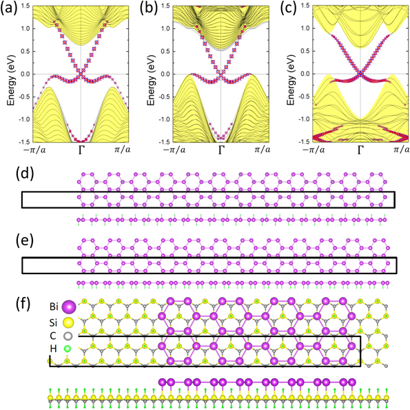
Figure 3. Band structure along the zigzag edge of (a) two-sided bismuthane, (b) one-sided bismuthane ribbon, and (c) a bismuthene ribbon on SiC(0001)- . (d)–(f) Atomic structures of zigzag ribbons for two-sided bismuthane, one-sided bismuthane, and bismuthene on SiC(0001)-
 , where the supercell is outlined with black solid lines. The contribution from the edge on the right is marked with red crosses, while that from the edge on the left is marked with blue circles. The yellow shadow denotes the bulk bands. Sizes of red crosses and blue circles are proportional to the contribution from the edges.
Download figure:
Standard image High-resolution imageBand structures of armchair edges are shown in figure 4. The width of freestanding ribbons with armchair edge is 74.9 Å (14  ) (figures 4(d) and (e)), while that of planar bismuthene on SiC(0001) is 37.45 Å (7
  ) (figure 4(f)). The band structures of the armchair edges of two-sided (figure 4(a)), one-sided (figure 4(b)) bismuthane, as well as bismuthene ribbon on SiC(0001)-
 (figure 4(c)) all exhibit similar edge states. Note that a small gap opens up at the Dirac nodes at the
  point in figure 4(c). This is attributed to finite size effects, reflecting interactions between the right and left edges.

Figure 4. Band structures along the armchair edges of (a) two-sided bismuthane ribbon, (b) one-sided bismuthane ribbon, and (c) bismuthene ribbon on SiC(0001)- . (d)–(f) are the corresponding atomic structures.
Download figure:
Standard image High-resolution image
We emphasize that the edge states for the zigzag as well as armchair cuts exhibit a remarkable single Dirac cone with the Dirac node lying inside the 2D band gap. This topological characteristic is the key for practically realizing many theoretical proposals as well as for applications [50–52] because the functional spin-polarized edge states can in this case be probed directly without the complicating effects of interference from bulk states.
4. Summary and Conclusions
Using first-principles computations, we predict a new class of 2D-TIs based on planar Bi and Sb honeycombs on SiC(0001) with band gaps as large as 0.56 eV. These honeycombs exhibit topologically protected edge states for both zigzag and armchair edges and harbor an isolated Dirac cone that lies within the bulk band gap, making them well-suited for accessing the long-sought topological transport regime. We also delineate how electronic structure is affected when hydrogen atoms are placed on only one side or symmetrically on both sides of the freestanding Bi/Sb films. Our analysis shows that effects of breaking the IS of freestanding planar Bi/Sb films by placing these films on the SiC(0001) substrate is similar to that of adsorbing hydrogen atoms on just one side of the film. Our predicted planar Bi and Sb honeycombs provide potential new materials platforms for exploiting exciting properties of 2D-TIs for room temperature applications.
Acknowledgments
FCC acknowledges support from the National Center for Theoretical Sciences and the Taiwan Ministry of Science and Technology under Grants Nos. MOST-101-2112-M-110-002-MY3 and MOST-101-2218-E-110-003-MY3. He is also grateful to the National Center for High-performance Computing for computer time and facilities. The work at Northeastern University was supported by the US Department of Energy (DOE), Office of Science, Basic Energy Sciences grant number DE-FG02-07ER46352 (core research), and benefited from Northeastern University's Advanced Scientific Computation Center (ASCC), the NERSC supercomputing center through DOE grant number DE-AC02-05CH11231, and support (applications to layered materials) from the DOE EFRC: Center for the Computational Design of Functional Layered Materials (CCDM) under DE-SC0012575. HL acknowledge the Singapore National Research Foundation for support under NRF Award No. NRF-NRFF2013-03.
Footnotes
- 4
After this work was completed, we recently became aware of an independent study of BiX and SbX films by Song et al [23] who consider passivation with X atoms on both sides of the film. In contrast, we consider one-sided H-passivation, which is the key for breaking the inversion symmetry and inducing large spin-splittings. The effect of the one-sided H-passivation is similar to that of the SiC substrate.