


Abstract
The presented experimental system is a barrier discharge system with plane parallel electrodes. The lateral surface charge distribution being deposited on the dielectric layer during each breakdown is observed optically using the well known electro-optic effect (Pockels effect). The temporal resolution of the surface charge measurement has been increased to 200 ns, and so for the first time it is possible to resolve the charge transfer to the dielectric surface in a single breakdown. In the present measurements, a patterned glow-like barrier discharge is investigated. It is found that the charge reversal in a single discharge spot (microdischarge) starts in the centre and then grows outwards. These experimental findings verify previously unconfirmed predictions from earlier numerical calculations and thereby contribute to a better understanding of the interaction between the plasma and the electrical charge on the electrodes.
Export citation and abstract BibTeX RIS

Content from this work may be used under the terms of the Creative Commons Attribution 3.0 licence. Any further distribution of this work must maintain attribution to the author(s) and the title of the work, journal citation and DOI.
1. Introduction
Dielectric barrier discharges (BD) are important and well-used plasma sources. The barrier inside the discharge volume prevents high-current arcing, therefore this plasma source a good candidate for applications at low-temperatures, such as plasma display panels [1], surface modification [2] and use in the biomedical sector [3, 4]. The measurement of surface charge deposited on the dielectric surface has recently gained attention because of its significant contribution to the overall behaviour of the discharge [5, 6]. A measurement with a high temporal resolution is especially desirable because the deposition mechanism of the surface charge endures only a fraction of the discharge cycle. Until now, the temporal resolution of the surface charge measurement has been too coarse to resolve a single breakdown in a laterally structured barrier discharge, thus, only breakdowns in diffuse discharges have been investigated and temporally resolved [6]. The best temporal resolution of the optical surface charge measurement obtained up to now is 600 ns in a plasma jet setup [7]. In the present work the temporal resolution is further increased. Hence, for the first time, a phase resolved surface charge measurement in a patterned barrier discharge is possible, being able to image the charge transfer within a single breakdown. The measurements presented in this article confirm the temporal behaviour of the charge deposition process that has been predicted by numerical simulations in [8].
The patterned barrier discharge under consideration in this work is observed in planar electrode arrangements with a high aspect ratio, i. e., with a small discharge gap compared to the lateral extension. Contrary to fast micro discharges that follow a streamer mechanism (as observed in [9, 10]), they behave electrically in a way usually observed in diffuse glow-like discharges (as observed in [11, 12]); the current pulse duration is in the microsecond range and the current density is several mA cm−2. However, in contrast to common glow-like barrier discharges, within some ten periods of the driving voltage the discharge becomes laterally patterned, i. e., split up into several discharge spots [13]. Through variation of the amplitude of the driving voltage the number of spots can be changed [8, 14]. Often, the discharge spots move across the discharge area and come to a rest after few minutes [15]. Laterally patterned discharges have been observed by several other authors, e. g. [14, 16–20]. Mostly, they appear in helium or helium mixtures in the parameter range of pressure p from 75 to 1000 hPa, frequency f from 50 to 200 kHz, electrode distance d from 0.5 to 3 mm, voltage  from 300 to 800 V.
2. Experimental setup
The discharge cell consists of two electrodes at a distance of  mm from each other. The first electrode is a dielectric bismuth silicon oxide (BSO) crystal (width:
  mm) that is on top of a grounded aluminium mirror. The second electrode is an indium tin oxide (ITO) coated glass plate with its electrically conducting side pointing to the gas gap. A sinusoidal voltage with a frequency of
  kHz is applied to the electrodes. The discharge is operated with helium at a pressure of
  hPa. For each measurement, the discharge is started with an applied voltage of approximately 250 V. The discharge area is then completely filled with moving discharge spots. In order to safely distinguish between the spots, their number is reduced by lowering the applied voltage to
  V. When the discharge spots have become stationary after a few minutes, the measurement is started.
The surface charge measurement is based on the polarisation shift of light that passes through the BSO crystal. Its optical properties cause a birefringence that is proportional to the electric field applied to the crystal. The electric field originating from surface charge on the BSO dielectric is measured with a setup sketched in figure 1. The light emitted by an LED ( nm) becomes linearly polarised. From the beam splitter, it is reflected by the aluminium mirror and finally passes an analyser in front of the camera. On its way, it is retarded by twice the phase retardation from the λ/8-wave plate and the additional phase shift
  according to the voltage drop U over the BSO crystal, with

In equation (1), n0 is the undisturbed refraction index ( ) of BSO, and r41 is its electro-optic constant that has been determined as 2.4 pm V−1 in a calibration measurement. The analyser in front of the high speed camera (Phantom Miro) is orientated perpendicular to the initial polariser. An optic band filter in front of the camera ensures that only the light emitted from the LED is detected. The intensity in front of the camera I(U) is expressed as
Here, I0 is the intensity of the light of the LED. In linear approximation, equation (2) becomes

Based on equation 3, let us define two intensities that correspond to characteristic situations during the measurement. The first is a surface charge free reference intensity  , where an external voltage drop
  on the BSO may be across the crystal, with

The other intensity corresponds to the actual measurement, where the voltage comprises of a contribution from the surface charge  as well as from external voltage
  , hence

To compute the voltage contribution  of the surface charge, the ratio
  is formed and resolved for
  :
:

Finally, the voltage  can be converted to the corresponding surface charge density sigma assuming a parallel-plate capacitor:

with a thickness of the BSO crystal of  mm, a dielectric constant of BSO of
  , and
, and  0 being the vacuum permittivity. In the measurements presented in this article, the reference image is recorded without external voltage (i. e.
  ), thus equation (7) becomes

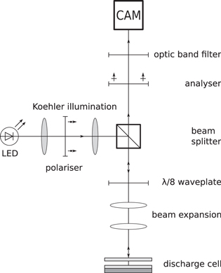
Figure 1. Sketch of the experimental setup.
Download figure:
Standard image High-resolution imageIn order to provide a temporal resolution of the measurement, the light coming from the LED is pulsed synchronously to the discharge driving voltage ( kHz) with one pulse per cycle. The camera has an exposure time of
  ms, so every camera frame averages over 200 LED pulses. To reduce the noise, 50 frames are recorded under the same conditions and averaged. Then, the LED pulse is shifted by
  200 ns relative to the discharge driving voltage and a new measurement cycle starts. The pulse width of one LED pulse is
  ns, so subsequent measurements overlap by 50% in time. The shape of the light intensity of an LED pulse is shown in figure 2. It can be approximated as a square pulse.

Figure 2. Profile of the light emission of the LED during one light pulse. The origin of the time axis corresponds to the trigger event for the LED controller.
Download figure:
Standard image High-resolution image3. Experimental results
In figure 3, the phase resolved development of the surface charge density along with the driving voltage and the current form is shown. The value for the surface charge represents an average over the whole BSO surface. In each half period of the applied voltage, one breakdown occurs. The mean surface charge density changes its value and polarity according to the occurrence of a current pulse. It behaves like the integrated current, which is also shown in figure 3.

Figure 3. Development of voltage, real current, and mean surface charge density during one period of the applied voltage. The charge represents the mean surface charge density of the whole BSO surface. The squares mark the selected times in figure 6.
Download figure:
Standard image High-resolution imageDuring each current pulse, a number of micro discharges are ignited simultaneously (figure 4(a)). Each micro discharge produces a surface charge spot as a 'footprint' that remains in the same position at least until the next discharge event (figures 4(b) and (c)). To examine the development of a charge spot for each temporal position, the surface charge density distribution is scanned for individual spots and cropped around them. From these croppings, a mean lateral surface charge density distribution for the spots is computed. In figure 5, the mean surface charge density distribution of a surface charge spot is shown for positive and negative polarity. Both were taken during temporally constant conditions, i. e., with no discharge taking place. They represent the state of surface charge just before a discharge starts. The peak surface charge densities are  nC cm−2 for the positive peak, and
  nC cm−2 for the negative peak. Also, the spots are usually on a charge offset, with
  nC cm−2 for the positive polarity and
  nC cm−2 for the negative polarity.

Figure 4. Overview of the whole electrode surface. (a) Photography of the discharge, (b) surface charge density distribution on the whole electrode at  , (c) surface charge density distribution on the whole electrode at
  .
.
Download figure:
Standard image High-resolution image
Figure 5. Mean surface charge density distribution for positive (left) and negative (right) polarity. The measurements were taken at  and
and  , when the charge density is temporally constant.
Download figure:
Standard image High-resolution imageIn figure 6, a typical deposition process of negative charge is shown. Again, the charge distribution is averaged over all spots in the discharge area. In the beginning, at  , there is a spot of positive surface charge, which has been deposited in the previous half-cycle. The charge profile through its centre is roughly Gaussian. During the charge deposition, the charge density is at first reduced globally, resulting in a shallower profile and a lower charge density offset (e. g. at
  ). However, the lateral charge deposition rate is not constant, instead it is most intense at the centre of the spot. Eventually, this results in a local minimum enclosed between two maxima (at
  ) in the charge density profile and the surface charge spot is successively radially replaced by its opposite charge. Finally, at
  , the charge profile reaches a state that is again roughly Gaussian, now for negative charge. Through the remaining low current density onto the dielectric surface, the charge distribution reaches the steady state as it is shown in figure 5 for 7.0 μs. The process of positive charge deposition takes place analogously to the deposition of negative charge with reversed sign.

Figure 6. Charge deposition in a current spot during the breakdown in the negative half-cycle. The times of recording for the displayed snapshots are marked in figure 3. Upper row: charge distribution of an averaged current spot. Lower row: representative cross sections through the centre of the current spot.
Download figure:
Standard image High-resolution image4. Comparison to numerical calculations
In the past, the only way to get insight into the development of the surface charge distribution in a laterally patterned discharge was to use theoretical considerations, mainly by numerical calculations. Therefore, we want to compare the newly found experimental results with previous numerical predictions. The memory effect induced by the surface charge spots has been well established theoretically and experimentally. However, the recharging of a charge spot starting in the centre and growing radially outwards is a newly discovered phenomenon that should also be reproduced in numerical simulations.
A numerical simulation of a single discharge spot in a plane parallel barrier discharge has been performed in [8] and the chosen physical parameters are similar to the present experiments. The underlying model is a simple drift-diffusion model comprising of continuity equations for electrons and singly charged ions as well as the Poisson equation for the electric field. The equations have been solved in three dimensions on a  grid with zero flux boundary conditions with x being the direction perpendicular to the electrodes and
  the plane parallel to the electrodes. To exploit the limited grid size efficiently, a quarter of a current spot has been placed into one corner of the discharge area. Through the mirroring effect of the zero flux boundary condition it is completed to a whole current spot.
The physical dimensions of the system under consideration are given by a discharge gap of d = 0.5 mm with both electrodes covered with a dielectric of thickness of a = 0.5 mm. The dielectric permittivity is  and its secondary emission coefficient is
  . The working gas is pure helium at a pressure of p = 200 hPa. The system is driven by a sinusoidal voltage with an amplitude of
  V and a frequency of f = 200 kHz. The gas and ion temperature is set to 25 meV, the electron temperature is 2 eV.
Starting from an initial spot-like surface charge distribution, several breakdowns of the numerical simulation were run until a steady state was reached. In figure 7, the applied voltage and the real current in a steady state discharge are shown. The discharge type determined from the current shape fits very well to the experimental data shown in figure 3. From the development of the electric field during the breakdown, the discharge type can be identified as a locally restricted glow-like discharge [8]. In figure 8, the development of the surface charge distribution during a single breakdown is shown. The relevant cutout of the numerical data has been mirrored at the boundaries in order to show the whole discharge spot, thus the diagrams in figure 8 are comparable to those in figure 6 for the experimental results. The times of the snapshots shown in figure 8 are marked in figure 7 with arrows, and as with the experimental results, the deposition of negative charge on the surface is shown. The initial surface charge density distribution (at  ) is quickly reduced in amplitude (at
  ). The current density is highest in the centre of the spot, hence the surface charge density there is eventually negative even though its surrounding is still positively charged (at
  ). Then, starting from the centre, the surface charge spot is radially replaced by negative charge. The breakdown with reversed polarity in the next half-period takes place qualitatively equally.
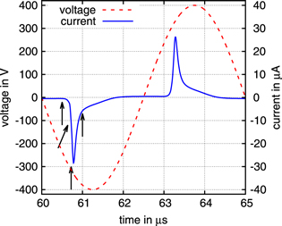
Figure 7. Driving voltage and real curent in the numerical simulation. The arrows depict the times of the graph in figure 8.
Download figure:
Standard image High-resolution image
Figure 8. Charge deposition in a current spot during the breakdown in the negative half-cycle in a numerical simulation. The upper row shows the smoothed surface charge distribution on the dielectric for different times, the lower row shows a corresponding cut along the z-axis. According to the zero flux boundary conditions, all graphs are mirrored at the origin.
Download figure:
Standard image High-resolution image
5. Conclusion
The high temporal resolution of the optical surface charge measurement presented in this article offers for the first time an insight into the charge development within a single breakdown of a patterned barrier discharge, i. e., the decrease and subsequent increase of surface charge in the course of a breakdown can be observed. On a global scale, regarding the overall discharge current from the electrical measurement and the spatially integrated surface charge from the optical measurement, a good quantitative agreement between the traditional electrical and the optical measurement is found. Regarding a single discharge spot laterally resolved, an interesting behaviour of the charge transfer was found: the charge reversal starts in the centre of a residual surface charge spot and grows radially outwards. The maximum of the real current peak coincides with a ring-shaped surface charge density distribution.
The experimental findings presented here support the predictions from previous numerical simulations. Although the discharge parameters are not equal they are very similar in the experiments and the numerical simulations, and both are well within the parameter range known for patterned discharges. From the simulation it is known that the discharge is started in the center of the surface charge spot because the electric field is highest there. While the discharge burns, a new, opposite charge is accumulated on the surface. Thus, the maximum of the electric field in the center of a discharge spot vanishes and instead a ring-shaped maximum with temporarily increasing radius emerges. As the current onto the dielectric surfaces moves along the electric field, the polarity of the charge spot is reversed starting from the center. In this way, the experimentally observed development of the surface charge distribution is qualitatively reproduced and comprehensible. Quantitatively, the numerical results are well within the same order of magnitude.
Acknowledgments
The authors are grateful to Uwe Meissner and Peter Druckrey for providing practical and technical assistance. This work was funded by the Deutsche Forschungsgemeinschaft, SFB TRR-24 (B14).