


Abstract
Microcavity exciton–polariton condensates, as coherent matter waves, have provided a great opportunity to investigate hydrodynamic vortex properties, superfluidity and low-energy quantum state dynamics. Recently, exciton condensates were trapped in various artificial periodic potential geometries: one-dimensional (1D), 2D square, triangular and hexagonal lattices. The 2D kagome lattice, which has been of interest for many decades, exhibits spin frustration, giving rise to magnetic phase order in real materials. In particular, flat bands in the 2D kagome lattice are physically interesting in that localized states in the real space are formed. Here, we realize exciton–polariton condensates in a 2D kagome lattice potential and examine their photoluminescence properties. Above quantum degeneracy threshold values, we observe meta-stable condensation in high-energy bands; the third band exhibits a signature of weaker dispersive band structures, a flat band. We perform a single-particle band structure calculation to compare measured band structures.
Export citation and abstract BibTeX RIS
1. Introduction
A two-dimensional (2D) kagome lattice, or a basketweave lattice [1], consists of interlaced triangles and exhibits a higher degree of frustration in comparison with other 2D lattices including square and triangular lattices [2]. Several materials in nature have been considered to have properties associated with the kagome lattice including jarosite [3], the second layer of adsorbed helium-3 on graphite [4] and a rare mineral known as herbertsmithite [2, 5]. The structure has been actively investigated in relation to spin frustration and associated magnetic phases. In addition, flat band ferromagnetism is one of the famous theoretical predictions regarding kagome lattices [6, 7]. A tight-binding band structure calculation of the 2D kagome lattice in the strong hopping energy regime including the nearest-neighbor tunneling terms predicts a completely flat band. In such a flat band the condensate order parameters become tightly localized at the potential dips [8]. The dispersionless band can be pictured to arise from quantum destructive interference around kagome hexagons, making clustered density distribution at the trap potential sites in real space.
Recently, several schemes were proposed to create flat bands in the 2D kagome lattice, utilizing metallo-photonic waveguides [9] or using photonic crystal structures [10]. Here, we explore microcavity exciton–polaritons in a 2D kagome lattice, whose potential is produced by depositing a thin metal film [11–14]. We present our photoluminescence properties in real- and momentum-space spectroscopy and images.
2. Exciton–polaritons and device fabrication
Exciton–polaritons are quasi-particles arising from the strong coupling between quantum well (QW) excitons and cavity photons, revealing quantum Bose nature, Bose–Einstein condensation [15–18] and superfluidity [19]. Our microcavity sample consists of three stacks of four GaAs/AlAs QWs sandwiched by 16 and 20 pairs of Ga0.8Al0.2As/AlAs as top and bottom distributed Bragg mirrors (DBRs). The cavity length is spatially varied so that the detuning values (Δ) between the exciton and the cavity photon energy can be tuned. The vacuum Rabi splitting at zero detuning (Δ = 0 V) is approximately 14 meV. In our experiment, we focus on detunings in the range Δ = 0 ∼ − 2.3 meV. Microcavity exciton–polariton systems have experimental advantages in accessing readily the in-plane momentum distribution of the polariton system by collecting leaked photon flux through the top DBR, due to energy and momentum conservation between the polaritons and external photons.
The metal-film deposition technique upon the grown microcavity wafers has been successful in producing in-plane periodic lattice potentials to influence excite-polariton condensates. It is simple but flexible to pattern readily various geometries in 2D. The underlying physical mechanism to produce the trap potential by this metal-film technique is that the cavity photon field is modified at the metal–semiconductor interface compared to the air–semiconductor interface. Owing to the metal film, the photon field vanishes at the metal–semiconductor region, whereas it decays into air in the bare semiconductor area. Therefore, the cavity length below the metal film is relatively squeezed; consequently, the photon energy is blue-shifted and the LP energy follows blue-shifted as well.
We applied negative resist to the wafer and used electron beam lithography to draw kagome lattice patterns in each 200 μm × 200 μm area. A 2D kagome geometry is patterned by arranging holes whose diameters are 1.5 or 3 μm with a 1:1 aspect ratio, namely the lattice constants are 3 and 6 μm, respectively. Figure 1 shows the 6 μm fabricated device. We deposit a thin metal film on top of the grown wafer by electron-beam lithography and lift-off [11, 12]. We deposited a 20/3 nm Ti/Au film, which produces about 200 μeV potential depth near the zero-detuning region [11–14].
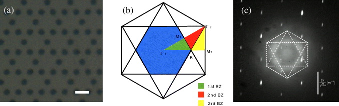
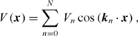
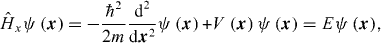
Figure 1. (a) A photograph of a fabricated kagome lattice device. The white bar scales the lattice constant 6 μm. The brighter area is where the thin metal film is deposited, and the darker circles are the potential traps. (b) The first (green), second (red) and third (yellow) BZs of the kagome lattice in a reciprocal space. High-symmetry points are denoted as Γ1, Γ2, M1, M2 and K. (c) Measured BZs of a device with a = 3 μm pumped at P/Pth ∼ 2.1 where the condensation threshold pump power Pth is about 7 meV. The white bar indicates the first BZ size.
Download figure:
Standard imageWe perform angle-resolved photoluminescence experiments at ∼ 4 K in a continuous-flow cryostat, measuring the spectra and images in real space and reciprocal space. A compact optical setup has been constructed utilizing Fourier optics to access the near- and far-field planes. We use a Ti:sapphire mode-locked laser to inject exciton–polaritons into the microcavity QWs. The tomographic momentum–energy dispersion relations in the Fourier planes enable us to construct the band structures of the 2D kagome device. A high numerical aperture (NA = 0.55) objective lens collects the emitted photons, which are fed into either a 0.75 m spectrometer or an imaging camera.
3. Band structures of a kagome lattice
The energy band structure and wavefunctions of states in a kagome lattice are calculated using a plane wave expansion of the potential. A kagome lattice potential V(x) can be described as a superposition of cosine waves
where kn are vectors in reciprocal space corresponding to the Fourier decomposition of  and
and  are the amplitudes. We find that N = 18 is enough to realize a kagome lattice shape approximately (figure 2(b) shows the kagome lattice potential profile using the 18-terms decomposition). We see that the kagome lattice is faithfully reproduced using the decomposition with clear potential dips at kagome points. Decomposing the potential into its Fourier components allows the Schrödinger equation,
to be written in Fourier space using the expansion  as
as
According to the Bloch theorem, each point k in the Brillouin zone (BZ) is coupled only to vectors  , which discretizes our Hamiltonian. We choose the region of
  in the first BZ and compute the band structure by diagonalizing our Hamiltonian. The size of the Hamiltonian Hk is infinite, since an arbitrary number of kn vectors can be added to the initial k point. However, due to the k2 diagonal elements of the Hamiltonian Hk , such high-momentum wavevectors are energetically suppressed, allowing us to impose a cutoff with negligible decrease in accuracy. We found that Hk within
  is sufficient to attain convergence to numerical precision.
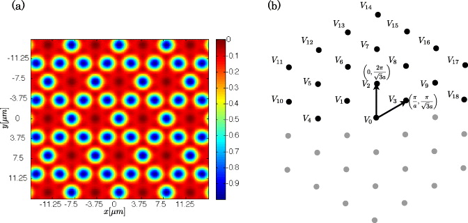
Figure 2. (a) A theoretical kagome potential profile in real space constructed by the 18 terms of Vn,  . (b) The decomposed Vn terms in a reciprocal lattice space with respect to V0. The chosen numerical values to create the kagome potential profile whose overall potential strength is 0.21E0 are in units of E0:V0 = −0.29, V1 = −V2 = V3 = −0.11, V4 = 0.67, V5 = V7 = V9 = −0.15, V6 = V8 = −0.07, V10 = V18 = −0.03, V11 = −V14 = V17 = −0.016, V12 = −V13 = −V15 = V16 = 0.025.
Download figure:
Standard imageThe result of such a calculation is shown in figure 3 for our experimental parameters. In the calculated results, the energy is normalized with  , where m = 9.1 × 10⁻³⁵ kg is the mass of an exciton–polariton under no potential, a is the lattice constant of a kagome lattice, and a band structure depends on the ratio of
  and V0 . In our experimental item, the potential depth V0 is fixed at 200 μeV due to a fixed potential depth the metal deposition technique makes [11–14].
  is changeable by choosing different lattice constants. The larger a becomes, the smaller E0 becomes, increasing V0 /E0 . Due to the lattice constant dependence of E0 the dimensionless depth of the potential V0/E0 can be varied by changing a .
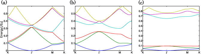
Figure 3. Calculated band structures along the high-symmetry points (Γ, M, K) of the lattice constant a = 3 μm (a), 6 μm (b) and 12 μm (c) in a single-particle plane-wave basis.
Download figure:
Standard imageThis means that the system is closer to the 'tight binding model' that predicts a completely flat band for larger lattices. We see this effect comparing figures 3(a) and (b), where the band structure becomes flatter for the larger sample, normalized to the same energy scale E0 . In particular, the third band most rapidly approaches a flat band, in agreement with previous works [10]. The remaining curvature of the third band can be attributed to the presence of next nearest-neighbor interactions, which break the degeneracy of the flat band. For a much larger lattice the third band becomes almost perfectly flat, as can be seen in figure 3(c) which assumed a = 12 μm. The energy scale of the band structure decreases with a; thus a trade-off between energy resolution and V0 /E0 must be made. For this reason we have chosen to work with a sample in the range of a = 3–6 μm .
4. Experimental results
The sample was pumped at an incidence angle of ∼ 60° by a 76 MHz mode-locking laser with a pump power of 15 mW, approximately twice the threshold for condensation. The laser spot size had dimensions of approximately 50 μm × 100 μm. Figure 1(c) shows a representative BZ taken with a device a = 3 μm. It clearly shows that a higher population of lower polaritons appears around the first BZ. The sharp emission peaks in a triangular pattern in figure 1(c) are due to the scattered pump laser signals, which give the scale of the first BZ. Figure 4 shows the pump power-dependent intensity plots at the high-symmetry points in the BZs. There is a nonlinear increase in the numbers of lower polaritons at each high-symmetry point, with a threshold around 10 mW.
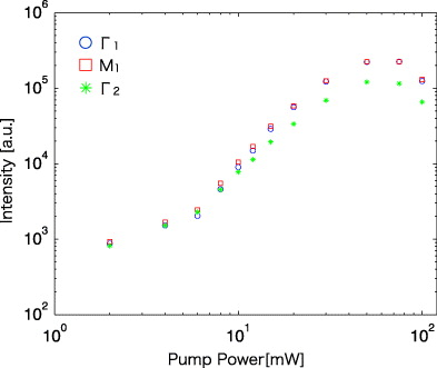
Figure 4. Intensity versus pump power at high-symmetry points in the a = 3 μm kagome lattice device.
Download figure:
Standard imageWe have experimentally measured the band structures of the first three bands from the tomography in the momentum plane. Figures 3(a) and (b) present the band structures of two devices with a = 3 and 6 μm, respectively. As the theoretical calculation shows, the bands in the a = 6 μm device are flatter. The flatter bands in the a = 6 μm device result from the fact that the fixed potential is renormalized by a four times smaller characteristic energy E0 in comparison with the a = 3 μm device. Due to the smaller potential strength and the broader energy spectral linewidth, we are not able to resolve the band gap between energy bands.
In figure 5, the signal strength of each band reveals the LP population distribution in the momentum space. For example, in the first band (left images), LP condensates are accumulated near Γ1, whose energy is lowest. Similarly, LP condensates are trapped near K points which are meta-stable points in the second and third bands. The black lines overlaid in the experimental results are the theoretically calculated band relations of the first, second and third bands, which match very well with experimental data.
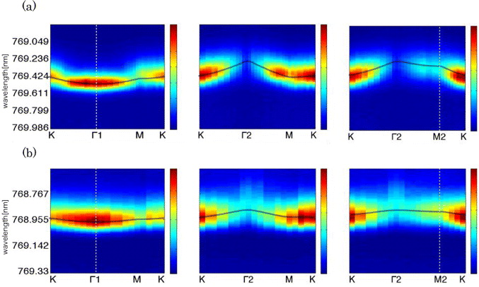
Figure 5. Measured energy dispersions along the high-symmetry points of the first (left), second (middle) and third (right) BZs within a = 3 μm (a) and 6 μm (b) kagome lattice devices. Black transparent lines are the calculated band structures.
Download figure:
Standard image5. Conclusion
We have successfully fabricated 2D kagome lattice structures with two different lattice constants by depositing a thin metal film on the grown GaAs-based microcavity structures. Photoluminescence experimental data exhibit the clear band structure of kagome lattice geometries, where meta-stable condensates of microcavity exciton–polaritons are formed above the quantum degeneracy threshold excitation values. In particular, exciton–polariton condensates show weaker dispersive energy relations with a larger lattice constant, which can be unambiguously explained by the renormalization of the energy scale in a given structure. We anticipate that with a stronger kagome lattice structure, the flat band can be produced in this system. The associated condensate order parameter of this flat band in the real space would be interesting to examine in future, which may reveal localization of condensates.
Acknowledgments
This work was supported by the Special Coordination Funds for Promoting Science and Technology, Navy/SPAWAR grant N66001-09-1-2024, the MEXT and the JSPS through the FIRST program.