


Abstract
We have studied the geometries, formation energies, migration barriers and diffusion of a copper interstitial with different charge states with and without an external electric field in the α-cristobalite crystalline form of SiO2 using ab initio computer simulation. The most stable state almost throughout the band gap is charge q = + 1. The height of the migration barrier depends slightly on the charge state and varies between 0.11 and 0.18 eV. However, the charge has a strong influence on the shape of the barrier, as metastable states exist in the middle of the diffusion path for Cu with q = + 1. The heights and shapes of barriers also depend on the density of SiO2, because volume expansion has a similar effect to increase the positive charge on Cu. Furthermore, diffusion coefficients have been deduced from our calculations according to transition-state theory and these calculations confirm the experimental result that oxidation of Cu is a necessary condition for diffusion. Our molecular dynamics simulations show a similar ion diffusion, and dependence on charge state. These simulations also confirm the fact that diffusion of ions can be directly simulated using ab initio molecular dynamics.
Export citation and abstract BibTeX RIS

Content from this work may be used under the terms of the Creative Commons Attribution-NonCommercial-ShareAlike 3.0 licence. Any further distribution of this work must maintain attribution to the author(s) and the title of the work, journal citation and DOI.
1. Introduction
The Cu–SiO2 system has attracted much interest because of the outstanding importance of these materials in the fabrication of microelectronic devices. SiO2 has found usage as a protective insulating layer in microelectronics due to its high resistivity, and Cu is used as an interconnect material in place of Al because it has a lower electrical resistivity and a higher electromigration resistance [1, 2]. However, Cu still interacts with SiO2, which can lead to diffusion of Cu ions through the dielectric layer and to metallization of SiO2. One result of this interaction is the degradation of the dielectric properties [3, 4].
On the other hand, the same process—electrochemical metallization (ECM) of dielectric thin films—is the basis for a new type of nonvolatile memory—resistive random access memory (RRAM) [5, 6]. This is under aggressive development, because it exhibits anticipated advantages with respect to current Flash memories. Advantages include higher memory cell density, faster read and write speeds and longer endurance or retention times [7]. A typical ECM RRAM cell is formed, for example, by a dielectric layer (SiO2) sandwiched between an electrochemically active anode (Cu) and an inactive cathode (Pt). The dielectric layer serves as a solid-state electrolyte for metal ions (Cu+). If the anode is oxidized by applying a high bias voltage, metal ions are dissolved in the electrolyte and can form a conductive bridge (nanometer-sized filament) between the electrodes. Application of the reverse bias will lead to a reduction of ions at the anode and dissolution of the metallic link [8].
It is clear that the mobility of Cu ions in SiO2 has a crucial influence on the speed of filament formation [9]. However, knowledge about Cu diffusion in SiO2 is quite limited and is available only for amorphous silica. For example, little is known even about the activation energy for diffusion, because the published experimental results are ambiguous. Initial work by McBrayer et al [10] reported experimental values of activation energy EA = 1.82 eV and of the diffusion coefficient D = 1.2 × 10⁻¹¹ cm2 s−1 at 450 °C. McBrayer et al also have used the approach described by Anderson and Stuart [11] to obtain a theoretical estimate. This calculation led to an activation energy EA = 1.2 eV. The difference between experimental and theoretical results in the paper is explained by the fact that the experimental value includes all processes contributing to the Cu transport, e.g. solution of Cu in SiO2 as well as oxidation of the anode. More recent experimental work reveals different activation-energy values lying between EA = 0.71 and 1.02 eV, and these values depend on sample preparation and microstructure. For example, the activation energy increases with increasing density of SiO2 [12].
Although the activation energy depends on the structure and density of SiO2, experiments show that Cu must be oxidized for diffusion to occur. McBrayer's work [10] demonstrated that copper can move easily through the oxide after a 450 °C anneal in both N2 and N2/H2 ambients. In contrast, very little or no Cu migration was observed even after annealing at 450–500 °C if the thermal treatment was carried out under vacuum. The same results were also observed by other researchers at even lower temperatures [13, 14]. This observation was explained by the presence of small amounts of oxygen in the N2 atmosphere, which is responsible for the oxidation of Cu. Kinetic Monte Carlo simulations, carried out by Pan and Subramanian [15, 16], led to a much lower value of the activation energy for bulk diffusion, equal to 0.4 eV. The same work also reported the activation energy for oxidation of Cu, which is higher and equal to 0.625 eV. The chemical and physical mechanisms of Cu transport in the dielectric are still unclear, but from the experimental results it follows that an important part of the Cu transport process is just oxidation at the anode [17].
It is surprising that the process of Cu diffusion, or simply the nature of Cu impurities in SiO2, has not yet been studied by ab initio techniques. Some work has been published about the Cu/SiO2 interface [18, 19], but there is nothing available about Cu impurities or diffusion (employing either density-functional theory (DFT) or empirical calculations). On the other hand, many works based on DFT have been published about impurities and diffusion of lighter elements, such as oxygen [20], carbon [21], nitrogen [22], boron [23–25] and aluminum [26]. Also much attention has been paid to simulations of native defects in different SiO2 modifications and their migration [27–30].
The purpose of this paper is to fill this gap. We present the results of first-principles calculations of migration paths and barriers of interstitial Cu atoms and ions in the α-cristobalite crystalline modification of SiO2. Also the effects of atomic volume and flipping of Si–O–Si linkages are discussed. The second part of the paper is focused on molecular dynamic (MD) simulations, which confirm our previous results. The effect of an external electric field on Cu migration is discussed in the third part. Although the experimentally used SiO2 is amorphous and not crystalline, we believe that the general conclusions we draw concerning defect chemistry are valid, and provide a framework for more extensive studies in the future even if the precise energy values depend on the local environment.
2. Computational methods
Our first-principles calculations were based on DFT within the local-density approximation (LDA), using the correlation energy of Ceperley and Alder [31, 32], as implemented in the Vienna ab initio simulation package [33–35]. The electronic orbitals were expanded in terms of plane waves with a maximum kinetic energy of 500 eV for structural optimization and with 300 eV for Bohn–Oppenheimer MD simulations. The electron–ion interaction was described by projector-augmented wave potentials [36, 37]. We used the Γ point for Brillouin-zone sampling. The criterion used for terminating the self-consistency iterations was that the total energy changed by less than 10−7 eV in succeeding iterations. The Gaussian smearing method, with a 0.1 eV smearing width, was used for the determination of partial occupancies for each wave function. Only for density of states (DOS) calculations were more accurate settings used, including the 3 × 3 × 3 k-mesh. Relaxation of the atomic structure was performed by the conjugate-gradient method, using the exact Hellmann–Feynman forces acting on atoms, and was considered to be converged after all forces dropped below 10 meV Å−1.
Diffusion pathways and migration barriers were computed using the nudged elastic band (NEB) method [38]. In applying this method, eight intermediate images were used to determine the converged minimum-energy paths between adjacent local energy minima. Another eight images were used for a precise determination of each transition state and local minima. In calculating charged defects, a homogeneous background charge was included to maintain overall charge neutrality in the periodic supercell. For integrating the equations of motion in MD simulations, a velocity Verlet algorithm with a time step of 2 fs was used. The temperature was controlled by the algorithm of Nosé. The method of applying a static electric field is in the spirit of the work of Neugebauer and Scheffler [39]. A linear electrostatic potential was added to the local potential, correcting the errors introduced by a dipole interaction between defects due to the periodic boundary conditions.
We used crystalline α-cristobalite (the P41212 structure) as the main model for SiO2, in part because it exhibits a density quite close to that of amorphous SiO2 [18, 40]. Our results for geometry optimization of α-cristobalite are summarized in table 1. At equilibrium we find that a = 4.9877 Å and c = 6.9456 Å for the tetragonal cell, in very good agreement with experiment [40] and previous calculations [18, 41, 42]. Also our results for the Si–O bond length and Si–O–Si bond angle agree very well with experimental results. The generalized gradient approximation (GGA) [43] is less successful than LDA in predicting structural parameters for SiO2 [41], which was also confirmed by our results (see the last column of table 1). The effect of the approximations used on the height of the barrier has also been tested. The GGA overestimates barriers by only about 10–15%. For this reason, we use LDA throughout this work. For calculating diffusion barriers, 2 × 2 × 2 supercells were used. The α-cristobalite supercells contained 32 SiO2 units (96 atoms) plus a single copper atom.
Table 1. Lattice constant, Wyckoff positions, Si–O bond lengths and Si–O–Si bond angle of α-cristobalite observed in experiment and obtained by LDA and GGA calculations. The Si Wyckoff position (4a) is shown as (u, u, 0) and the O Wyckoff position (8b) as (x, y, z).
| α-cristobalite | ||||
|---|---|---|---|---|
| Parameter | Experimenta | Prev. calc.b | LDA | GGA |
| a (Å) | 4.9717 | 4.9750 | 4.9877 | 5.0638 |
| c (Å) | 6.9222 | 6.9070 | 6.9456 | 7.0587 |
| Si (u) | 0.3003 | 0.3005 | 0.3000 | 0.2969 |
| O (x) | 0.2392 | 0.2389 | 0.2391 | 0.2401 |
| O (y) | 0.1044 | 0.1058 | 0.1043 | 0.0990 |
| O (z) | 0.1787 | 0.1801 | 0.1789 | 0.1767 |
| Si–O(1) (Å) | 1.6034 | 1.6056 | 1.6091 | 1.6259 |
| Si–O(2) (Å) | 1.6026 | 1.6062 | 1.6080 | 1.6254 |
| S–O–Si (deg.) | 146.5 | 145.8 | 146.3 | 147.6 |
For MD simulations we used a slab model created from a 2 × 2 × 3 SiO2 supercell. Our computational cell contained 48 SiO2 units (144 atoms) in the slab centered in the middle of the supercell and a single copper atom. Dangling bonds on both surfaces were saturated by 16 hydrogen atoms, which were fixed in their equilibrium positions for all our MD simulations. The vacuum distance, necessary for the separation of slabs in periodically repeated cells, was set to 13.5 Å. The use of a slab model is necessary for calculations with an applied external electric field. The field was applied in a direction perpendicular to the slab plane (in the z-direction).
To determine the stability and electrical effects of Cu impurities, we estimated the formation energies of Cu in an interstitial position for different charge states as well as their transition levels. The formation energy Ef is obtained as follows:

where Etot(SiO2 + Cu) is the total energy of the SiO2 supercell with interstitial Cu, Etot(SiO2) is the total energy of the same supercell without the Cu defect and Etot(Cu) is the total energy per atom of Cu with the fcc structure. q is the charge of the supercell with the defect and EF is the Fermi-level position within the band gap. Because we consider only interstitial impurities, the number of Si and O atoms is the same before and after the creation of defects, and the formation energy does not depend on the chemical potential of Si or O.
Transition-state theory (TST) [44–47] allows us to determine the diffusion coefficient D directly from the energy-barrier calculation. The diffusion coefficient of the atomic interstitial is generally expressed by the Arrhenius formula as

where D0 is the temperature-independent pre-exponential factor, T is the temperature and kB is the Boltzmann constant. EA is the activation energy for diffusion and is equivalent to the minimum height of the migration barrier, which the diffusing particle must overcome from an equilibrium site to advance along the diffusion path to another equilibrium site. The pre-exponential factor can be calculated using the expression

where α is the dimensionality of space, l is the elementary jump length, g is the number of equivalent diffusion paths and ξ is the dynamical correction factor, which accounts for correlated (and reverse) diffusion jumps and is usually set to unity, as it is in the present paper. The rest of the formula describes the fraction of the total partition functions of the ground state and of the transition state, which can be written with use of the harmonic approximation as a product of the vibrational frequencies. The ν(0)i and ν(s)i are the normal-mode frequencies of vibration in the ground state and the activated state, respectively. N is the number of vibrating atoms. Because the potential energy has negative curvature along the reaction coordinate, an imaginary vibrational mode is obtained at the saddle point. Thus, there is one real normal mode less at the saddle point than in the ground state. For frequency calculations only 15 atoms were allowed to vibrate, including a Cu atom, 4 neighboring Si atoms and 10 neighboring O atoms. Quantum mechanical zero-point corrections [48] have been neglected due to their small contribution.
Another way to calculate the diffusion coefficient D is by using the Einstein relation

where t is the simulation time and 〈Δr(t)2〉 is the mean-square displacement of the Cu ion in SiO2, which can be obtained from MD simulation. This mean is an average motion of the Cu ion from different independent simulations and is estimated by the function

where M is the number of simulations, ri(0) is the position of the Cu ion at the beginning of the simulation and ri(t) is the position of the Cu ion at time t. The diffusion coefficient is calculated by fitting 6tD to 〈Δr(t)2〉, using D as a fitting parameter.
3. Results
3.1. Cu impurity in SiO2
Because experiments reveal the importance of Cu oxidation for its diffusion, we performed calculations for both neutral and charged Cu atoms with charges q = + 1, +2 and −1. In addition, Cu with a partial charge q = + 0.5 was included in our calculation. The Cu interstitial occupies the cavity surrounded by 12 SiO4 tetrahedra (see figures 1(a) and (b)), and is located in a symmetrical position between two O atoms. The position of Cu does not depend much on the charge state, as the difference is only 0.1 Å. Because a weak attractive electrostatic interaction was observed between the neutral Cu atom and both of the nearest O atoms, the α-cristobalite lattice is only slightly distorted. The distance of these O atoms is 2.337 Å and the distance of next-nearest neighbors is 2.613 Å. We consider only an interstitial Cu impurity in our calculations, because this small lattice distortion and attractive interaction lead us to the assumption that the α-cristobalite lattice contains enough space and the diffusion can be realized by the interstitial mechanism rather than exchange. The interaction between Cu and O is much stronger for the Cu+ ion and also the distance between Cu and O becomes much smaller (1.987 Å), and the distortion of the lattice is much stronger. The O–Cu+–O interaction can be recognized from the bonding electron density, which is defined as the difference between the self-consistent electron density of our system and a superposition of the electron densities of free atoms arranged in the same structure. The plot of the bonding electron density is shown in figure 1(c) for the plane corresponding to the Cu+ ion and both interacting O atoms. For Cu with a charge q = + 2, the interatomic distances are basically the same as for q = + 1. On the other hand, repulsive forces were observed for negatively charged Cu− ions.
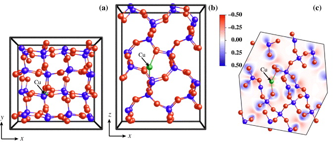
Figure 1. Stable configuration of a Cu+ ion in the α-cristobalite lattice from top (a) and side (b) points of view. The plot of bonding electron density (c) shows the electrostatic interaction of Cu+ with two nearest O atoms. The Cu ion is denoted by the green sphere. O and Si atoms are denoted by red or blue, respectively.
Download figure:
Standard imageA detailed analysis of interaction between Cu and O can be performed based on the DOS. Figure 2(a) shows the DOS of pure α-cristobalite without any defects and impurities. States in the valence band are separated into two bands. The first band corresponds to the bonding states and is occupied by O 2p and Si 3p electrons. The second band corresponds to the nonbonding states, which are occupied mainly by O 2p electrons. The antibonding states in the conduction band are separated from the valence band by a band gap with width 5.7 eV. The predicted width of the band gap is much smaller than the experimental value of 8.9 eV [49], but is consistent with other ab initio calculations which have not included any non-local corrections for the exchange correlation energy [30, 50, 51].

Figure 2. DOS for α-cristobalite without any defects (a) and with copper in states with charge q = 0 (b), q = + 0.5 (c) and q = + 1 (d). Energies are shown with respect to the Fermi level.
Download figure:
Standard imageAn added Cu atom introduces states in the band gap, as generally expected (see figure 2(b)). The highest occupied state is located 1.1 eV below the conduction-band minimum and 4.5 eV above the valence-band maximum. The nonbonding valence band, corresponding to the O atoms close to Cu, is narrower than the band from other O atoms due to the interaction of nonbonding electron pairs with Cu. This interaction becomes stronger when positive charge is placed on Cu. For q = + 0.5, the nonbonding band of O far from Cu is about 0.5 eV wider than the band of O which interacts with Cu (see figure 2(c)). The Cu state is only half occupied and is shifted closer to the conduction-band minimum. When a whole electron is removed from the system (q = + 1), the highest Cu state in the band gap is now unoccupied and is shifted very close to the antibonding states. Interaction between Cu and neighboring O atoms now takes place in the gap between the bonding and nonbonding states (see figure 2(d)).
To estimate the stability of Cu defects in α-cristobalite, we have calculated the formation energy according to equation (1). Because we are interested in the effect of the charge state, the formation energies are plotted in figure 3 as a function of the Fermi level EF, which varies from the valence-band maximum to the conduction-band minimum across the band gap of α-cristobalite. The results clearly show the stability of positively charged Cu with q = + 1 in almost the whole band gap up to the Fermi level at 4.59 eV. After this point, the negatively charged Cu becomes the more favorable state. The state with charge q = + 2 is preferred only in the bottom of the band gap, up to the Fermi level at 0.48 eV. Since the states with q = + 2 and −1 are not dominant, the state with q = + 1 will be taken into account in the rest of this work. However, the unstable states with q = 0 and +0.5 are also included in our paper in order to explain the effect of partial oxidation of Cu.
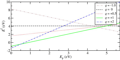
Figure 3. Formation energy of a Cu impurity as a function of the Fermi level.
Download figure:
Standard image3.2. Height of the barriers and diffusion coefficients
After finding the stable geometry of Cu in the α-cristobalite lattice, we can approach the estimation of diffusion pathways between two equivalent positions and of the energy barriers along this path. The trajectory of a Cu atom is shown in figure 4(a). A Cu atom can easily move along the bond networks of SiO2. The trajectory is independent of the charge on Cu. However, the shape of the migration barrier depends on the charge, as shown in figure 4(b). The barrier for neutral Cu has a typically symmetrical shape, with one maximum corresponding to the transition state in the middle of the diffusion path. The height of the barrier corresponds to the activation energy EA for diffusion and is equal to 0.18 eV.
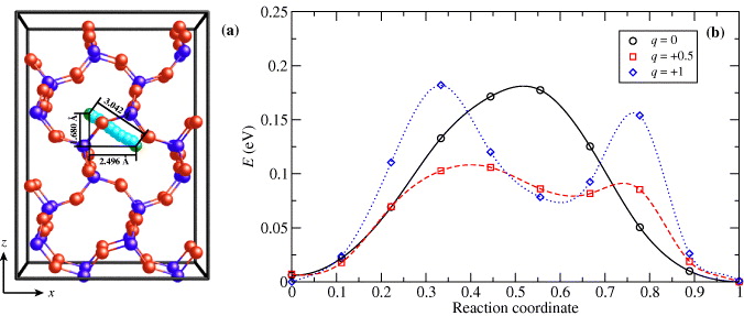
Figure 4. Positions of the Cu atom along the diffusion pathway (a) in the α-cristobalite lattice. Both equilibrium positions are denoted by green color and other positions along the path are denoted by light blue color. Migration barrier of Cu diffusion along the diffusion path (b) for different charges q on Cu.
Download figure:
Standard imageThe barrier changes when positive charge is added. For a charge of q = + 0.5, the diffusion barrier is significantly asymmetric, because the position of the transition state is shifted closer to the equilibrium position and a plateau can be found in the middle of the path. Also the height of the barrier becomes lower, about 0.11 eV. The change in shape is more pronounced when a whole electron is removed from the system (q = + 1). The activation energy is now equal to 0.18 eV, which is the same value as for the neutral impurity case. The energy profile along the path now contains two maxima with transition states and one minimum in the middle, where a new metastable state is situated.
This change of shape can be explained by an increasing interaction of a Cu ion with two nearest O atoms. When the Cu starts moving, these two weak bonds are broken and two new ones are created. For neutral Cu, the interaction is weak and Cu can continuously move through the lattice and other atoms do not change their positions. For charged impurities, the interaction is stronger and both O atoms follow the Cu because the distances remain the same as at the beginning of the pathway. The first bond is broken after traversing a quarter of the path, and a bond with a new O is created. This metastable state in the middle of the path then corresponds to the situation where the Cu interacts with one O near the starting position and with a second O near the final position of the path. However, both O atoms are now too close to Cu, which makes the energy of this state higher than in equilibrium, and another rearrangement of bonds is necessary. This happens approximately at the third quarter of the path. This effect of interactions of Cu with different O atoms can be recognized from the diagram of interatomic distances along the diffusion pathway (see figure 5).

Figure 5. Interatomic distances between Cu and other atoms along the diffusion pathways. The solid lines with full symbols correspond to the neutral Cu atom and the dashed lines with open symbols denote Cu with charge q = + 1. The corresponding atoms in systems with different charge states on Cu are represented in the same color.
Download figure:
Standard imageThe values of activation energies, as well as jump lengths and diffusion coefficients, are summarized in table 2 for different values of the charge q on Cu. Distances between equilibrium positions do not differ too much, because the structure along the diffusion pathways does not depend on charge, but the interatomic distances are shorter (see figure 5). On the other hand, charging has a strong effect on the diffusion constant. The smallest value of the pre-exponential factor D0 is observed for neutral Cu, and increases with increasing charge. This corresponds to the experimental observation that diffusion is possible only in an oxidizing atmosphere [13, 14]. However, due to the small migration barrier for q = + 0.5, the diffusion at 500 K for this case is faster than for q = + 1, which can be explained by a stronger interaction between Cu and O.
Table 2. Activation energies of diffusion EA, jump lengths l, diffusion pre-exponential factor D0 and diffusion constant D500 at 500 K for different charges q on Cu.
| q | EA (eV) | l (Å) | D0 (cm2 s−2) | D500 (cm2 s−2) |
|---|---|---|---|---|
| 0 | 0.18 | 3.042 | 4.5×10⁻⁵ | 7.8×10⁻⁷ |
| +0.5 | 0.11 | 3.049 | 1.5×10⁻⁴ | 1.2×10⁻⁵ |
| +1.0 | 0.18 | 3.054 | 3.8×10⁻⁴ | 5.8×10⁻⁶ |
Our theoretical results for EA and D differ from experimental findings, because experiments show the diffusion constant D723 = 1.2 × 10⁻¹¹ cm2 s−1 at 450 °C (723 K) and an activation energy between 0.71 and 1.82 eV. We predict at the same temperature a much larger value of D723 = 2.5 × 10⁻⁵ cm2 s−1 for q = + 0.5 and D723 = 2.0 × 10⁻⁵ cm2 s−1 for q = + 1. However, all the available data are based on measurements in amorphous SiO2, while our simulations are for the crystalline form. Unfortunately, experimental results for the crystalline phase of silica are unavailable in the literature. We suppose that, although the densities of the amorphous form and α-cristobalite are very similar, the distribution of mass in the amorphous form is not uniform. Accordingly, the amorphous phase contains regions with lower densities where the diffusion is relatively easy, and also contains regions with a higher density where the diffusion is slower. The net diffusion coefficient is affected mainly by the regions with higher density. The experimental values of activation energies also include all processes such as solution of Cu in SiO2 or its oxidation. Another open question is diffusion through the metal/SiO2 interface and interactions of Cu ions with defects in the insulator. However, our value of EA is not too far from the value EA = 0.4 eV obtained from kinetic Monte Carlo simulations [15, 16]. On the other hand, our values can be compared with previous ab initio calculations of hydrogen diffusion in α-cristobalite [52]. The activation energy for H estimated in this work, equal to 0.2 eV, is very similar to our result for Cu. The pre-exponential factor of H diffusion is even about two orders of magnitude bigger, D0 = 8.1 × 10⁻³ cm2 s−1.
3.3. Density dependence of the barrier heights
For a better understanding of the influence of interatomic distances and of the density of SiO2 on diffusion barriers, we have also investigated the dependence of barrier heights on the volume of the supercell. It is not surprising that the height of the barrier decreases with increasing volume (see figure 6), because Cu has more space for motion. More interesting is the influence of the volume on the shape of the barrier. For neutral Cu, we observe only a slightly increasing asymmetry of the barrier, as shown in figure 6(a). However, for charged states, the volume effect is crucial. The barrier for q = + 0.5 is shown in figure 6(b). If the volume is expanded, the shape is changed and it looks more like the profile for q = + 1 at the equilibrium volume, whereas when the volume is contracted, the shape of the barrier remains the same, only the activation energy is higher. On the other hand, expansion of the volume does not change the barrier profile for q = + 1, while contraction does (see figure 6(c)). The profile for the contracted volume is similar to the profile for q = + 0.5. It follows that the expansion or contraction of volume has a similar effect as increasing or decreasing the charge. This can be explained by an increasing flexibility of Si–O–Si linkages with increasing volume and decreasing density. If the bonds are flexible enough, a smaller charge is sufficient for Cu interaction with O atoms and local distortion of the SiO2 structure.
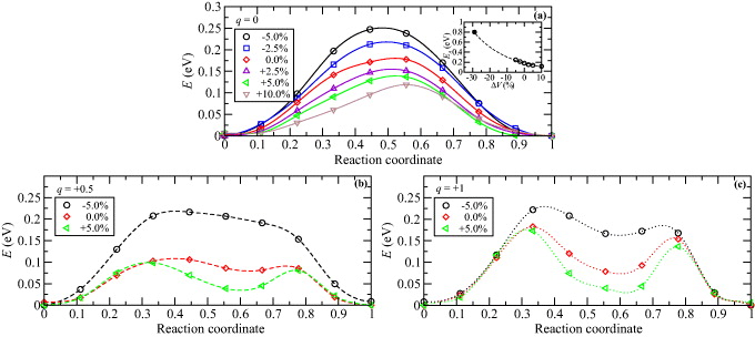
Figure 6. Migration barrier for Cu with a charge q = 0 (a), +0.5 (b) and +1 (c) along the diffusion pathways for different volumes of the supercell. The inset (a) shows the height of the migration barrier EA as a function of volume change ΔV . Open circles correspond to the values from NEB calculations. The dashed line is an exponential extrapolation to smaller volumes. The full circle denotes our estimation of the volume compression for the height of the barrier, which corresponds to the experimental diffusion coefficient.
Download figure:
Standard imageThese results also allow us to better understand the conditions in amorphous SiO2. We can estimate with the help of the TST how high the barrier has to be for obtaining the diffusion constant observed in experiments. We will assume for the moment that the diffusion constant depends only on temperature and activation energy. The experimental value D723 = 1.2 × 10⁻¹¹ cm2 s−1 approximately corresponds to EA ≈ 0.8 eV, which also lies in the range observed in experiments. This means that our pre-exponential factors D0 are in good agreement with experiments. If we use an exponential function for extrapolation of our calculated barrier heights from figure 6(a), we can estimate the density of the amorphous phase in regions where diffusion is difficult. This extrapolation gives us the density, which corresponds to a 25–30% volume compression (see the full circle in the inset of figure 6(a)). This is a reasonable number, because the density of SiO2 depends on the phase and varies between 1.8 g cm−3 for porous materials and 4.3 g cm−3 for stishovite. The average value for amorphous silica is 2.2 g cm−3. Our model for α-cristobalite exhibits a density equal to 2.3 g cm−3. The volume compression, which corresponds to the density of α-quartz (2.7 g cm−3), is equal to ∼15%. Our estimated 25–30% compression almost corresponds to the density of the high-pressure form coesite (2.9 g cm−3) or small amorphous clusters [53]. This is only a rough estimation, because it does not take into account different bonding conditions, which also affect diffusion. However, it can provide a picture of the mass distribution in amorphous SiO2 and can also better explain the difference between our theoretical values for the crystalline phase and the experimental values for the amorphous phase of SiO2.
3.4. Decreasing the barrier by flipping the oxygen atoms
The flexibility of Si–O–Si linkages has another effect on the Cu diffusion. Because Si and O atoms oscillate about their equilibrium positions and the Si–O–Si linkages can be 'flipped' even at very low temperature [54], we have also investigated the influence of the flipping on the height of the barrier. This flipping is realized by the torsion of an SiO4 tetrahedron when the flipped O atom changes its position by approximately 1 Å and that of one of the adjacent Si atoms by about 0.5 Å. However, the flipped geometry is unstable for single Si–O–Si linkages only. For the calculations, it can be stabilized by flipping all Si–O–Si linkages in one row (yellow atoms in figure 7(a)). The barrier for this associated flipping of O atoms is about 0.26 eV and the final geometry has a total energy higher by about 0.024 eV. The space created by the flipped O allows for easier motion of Cu, because the barrier along the migration path is lower. Barriers are shown in figure 7(b) for the flipped and non-flipped geometries. The barrier is lower by about 0.05 eV for neutral Cu, the same as that for Cu with a charge q = + 0.5. In reality, this flipping can be caused by thermal vibrations and can make diffusion through SiO2 much easier and faster.
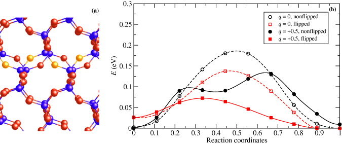
Figure 7. Part of the α-cristobalite lattice with flipped O atoms represented in yellow color (a). Migration barrier for Cu diffusion along the diffusion pathways (b) for different charges q and different geometries of the α-cristobalite lattice with and without flipped O atoms.
Download figure:
Standard image3.5. Molecular dynamics
In order to better understand the mechanism of Cu transport through SiO2, which takes place in the SET process of RRAM, we prepared also a series of MD simulations at 500 K, and with simulation times of 66 ps. We started our calculations with an ideal defect-free supercell without the Cu atom for verification of the stability of the lattice geometry at 500 K. Figure 8 shows the x, y and z coordinates of two chosen Si and four adjacent O atoms. The α-cristobalite lattice was stable at 500 K for the whole simulation time. All Si and O atoms oscillate about their equilibrium positions and defect creation was not observed. Only 'flipping' of Si–O–Si linkages occurred (see figure 7(a)), which was introduced in the previous section. These flipping events are easily recognizable in figure 8.
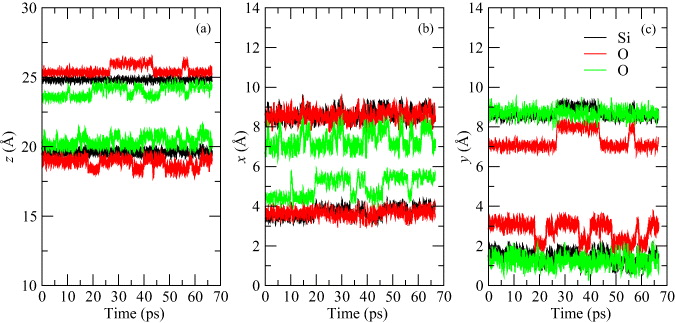
Figure 8. The z (a), x (b) and y (c) coordinates of two different Si atoms (black curves) and four different O atoms (red and green curves) as a function of time for MD simulation at 500 K in an α-cristobalite supercell without Cu atoms and any other defects.
Download figure:
Standard imageIn the next step, we have inserted one Cu atom into the interstitial equilibrium site in our supercell. Simulations were prepared for neutral Cu and with a charge state q = + 0.5, because it exhibits a lower migration barrier than charge state q = + 1. The x, y and z coordinates of Cu are shown in figures 9 and 10. We prepared three independent simulations for each charge state: q = 0 and +0.5. The simulation for a neutral Cu atom exhibits only a few random jumps between neighboring interstitial positions or to the next interstitial position (see figure 9). Jumps are infrequent and the time between the jumps is usually more than 30 ps, which is inadequate for extracting quantitative results from these simulations. On the other hand, the frequency of jumps of the ion is much higher (see figure 10). Oxidized Cu can move through the α-cristobalite lattice very easily. During these simulations, no lattice distortions or defect creations were observed other than the Si–O–Si bond flipping.
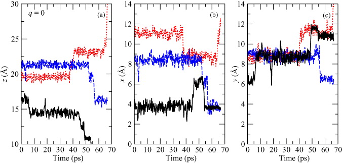
Figure 9. The z (a), x (b) and y (c) coordinates of a neutral Cu atom as a function of time for MD simulation at 500 K in α-cristobalite. Results are shown for three independent simulations denoted by different colors—black, red and blue.
Download figure:
Standard image
Figure 10. The z (a), x (b) and y (c) coordinates of a Cu ion with a charge state q = + 0.5 as a function of time for MD simulation at 500 K in α-cristobalite. Results are shown for three independent simulations denoted by different colors—black, red and blue.
Download figure:
Standard imageAfter the analysis of our data, we calculated the mean-square displacement 〈Δr(t)2〉 of the Cu ion at SiO2. The mean-square displacement as a function of simulation time t is shown in figure 11(a) for total motion and also for motion in each direction separately. These results show that the x and y directions are slightly preferred for motion than the z-direction. In this way, we also estimated the diffusion coefficient of the Cu ion in α-cristobalite to be D500 = 2.6 × 10⁻⁵ cm2 s−1, which is in very good agreement with the value D500 = 1.2 × 10⁻⁵ cm2 s−1 obtained with the help of the TST. As was mentioned before, our values are much higher than the experimental value of D723 = 1.2 × 10⁻¹¹ cm2 s−1 [10]. On the other hand, our results for MD simulations nicely confirm the fact that a necessary condition for diffusion is oxidation of Cu first [17], because our simulations show that the motion of Cu atoms is much slower than the motion of Cu ions.

Figure 11. The mean-square displacement 〈Δr(t)2〉 of the Cu ion with a charge state q = + 0.5 as a function of time (a) calculated as an average from MD simulations shown in figure 10. The black dashed lines correspond to the fitting function from equation (4). Also the mean-square displacements of motion in the x, y and z directions are shown. Trajectories of the Cu ions in α-cristobalite (b, c). Results are shown for three independent simulations, which are shown in figure 10 and are denoted by different colors—black, red and blue.
Download figure:
Standard imageIt is necessary to mention that a supercell with a slab of SiO2 has been used for MD simulations due to an investigation of the effects of an external electric field presented later. The conditions for diffusion can be different near the surface corresponding to the middle of the slab, because the Cu atom exhibits slightly higher total energy, approximately about 0.02 eV, if it is placed close to the surface. Our results shows the motion of the Cu ion is mainly in the x- and y-directions, which can be caused by this surface effect. However, we assume that this has no influence on our calculations of diffusion coefficients.
To illustrate the diffusion mechanism of a charged system, the trajectory of the Cu ion in SiO2 is shown in figures 11(b) and (c). The trajectory is shown from the top (b) and side (c) points of view. We used the projection of the ideal α-cristobalite lattice from the beginning of the simulation as a background for easier identification of motion between equilibrium interstitial sites. The motion between two adjacent interstitial sites is always realized in the direction parallel to one of the Si–O–Si bonds (see figure 11(b)) and corresponds to the migration path described in section 3.2 (compare figures 4(a) and 11(b)).
3.6. Interaction with the external electric field
Because the mechanism of the resistive switching process is enforced by the application of a bias voltage on the electrodes, we were interested also in how our previous results can be affected when an external electric field is applied. Using the Neugebauer and Scheffler method allows us to apply a field only on the slab of the SiO2 and not on the bulk, because periodic boundary conditions are used in our calculations. When the slab of SiO2 is introduced into the electric field, it induces a weak polarization of electron density on O atoms. The electron density differs by not more than 0.004 electron Å−3. If a Cu ion is introduced in the slab, the polarization is screened in the part of the slab on the side of the anode. Changes in structure were not observed and the atomic position remains the same.
However, the electric field changes the migration barrier. The shape and the height of the barrier remain basically the same but energies along the path are shifted with respect to the field gradient. This shift of energy is shown in figures 12(a) and (b) for charges q = + 0.5 (a) and q = + 1 (b) and for two different magnitudes of field:  (b) and
  (a). Energies are shown with respect to the energy of the equilibrium position in the beginning of the migration path. The barrier, where the field is not applied, is shown for comparison. Because we used the slab of SiO2, these displayed barriers slightly differ from the barriers calculated in bulk. The variation is caused by the presence of a surface close to the migration path, although the migration path has been located in the middle of the slab. However, we believe that these differences can be neglected.
Figure 12. The migration barriers for the Cu ion with charge state q = + 0.5 (a) and +1 (b) and within the external electric field with magnitude 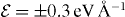 (a) and ± 0.2 eV Å−1 (b). The barriers calculated without an external field are also shown. The difference of total energies ΔE between the first and last points of the migration path as a function of the magnitude of the applied field
  (c).
(c).
Download figure:
Standard imageAs was mentioned before, the driving force for Cu motion is the gradient of electrostatic potential. Therefore we have plotted the energy differences between the first and last points of the migration path as a function of the magnitude of the external field. These results are shown in figure 12(c) for q = 0, +0.5 and +1. The dependence on the magnitude of the field is strongly linear in the whole interval of our study. As also follows from this figure, an external field does not have any significant effect on the migration barrier when the Cu atom is neutral.
We prepared another set of MD simulations again at 500 K. These simulations should help us to prove that Cu motion in SiO2 can be driven by the switching of polarity of the external electric field. Because the barrier is lowest for q = + 0.5, we chose this value. We also used a relatively strong external field:  , because a strong field effect should decrease the simulation times. Our simulation was restricted to the central third of the slab to avoid surface effects, which can have an influence on the migration. When the Cu atom moved out of this region and crossed the hypothetical planes through the slab, the polarity of the field was switched. This causes the Cu ion to move in the opposite direction. When the Cu ion reaches the second side of the region the whole process is repeated. The distance between these two sides is 7.2 Å and there are four equilibrium positions along the shortest path. The average time which the Cu ion needs for one way to cross over this region is approximately 27 ps. We repeated three independent simulations with a simulation time equal to 170 ps for each. During each run the field polarity was switched approximately five times. The result for one of these simulations is shown in figure 13(a). Because the field gradient is oriented in the z-direction, only the
z coordinates of the Cu ion are displayed as a function of simulation time. Both the horizontal dashed lines correspond to edges of the simulation region and to the planes through the slab, where the polarity of the field was changed when they were crossed by a Cu ion. The different field polarities are denoted by the white and gray areas as well as the plus and minus symbols.
, because a strong field effect should decrease the simulation times. Our simulation was restricted to the central third of the slab to avoid surface effects, which can have an influence on the migration. When the Cu atom moved out of this region and crossed the hypothetical planes through the slab, the polarity of the field was switched. This causes the Cu ion to move in the opposite direction. When the Cu ion reaches the second side of the region the whole process is repeated. The distance between these two sides is 7.2 Å and there are four equilibrium positions along the shortest path. The average time which the Cu ion needs for one way to cross over this region is approximately 27 ps. We repeated three independent simulations with a simulation time equal to 170 ps for each. During each run the field polarity was switched approximately five times. The result for one of these simulations is shown in figure 13(a). Because the field gradient is oriented in the z-direction, only the
z coordinates of the Cu ion are displayed as a function of simulation time. Both the horizontal dashed lines correspond to edges of the simulation region and to the planes through the slab, where the polarity of the field was changed when they were crossed by a Cu ion. The different field polarities are denoted by the white and gray areas as well as the plus and minus symbols.
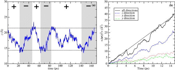
Figure 13. The z (a) coordinates of a Cu ion with a charge state q = + 0.5 and within an external electric field with magnitude  as a function of time for MD simulation at 500 K in α-cristobalite. The vertical lines indicate edges of the simulation region and conditions for the switching of the field polarity. The + and − symbols and the white and gray fields correspond to different field polarities. The mean-square displacement 〈Δr(t)2〉 of the Cu ion as a function of time (b) calculated as an average from 15 MD simulations. The black dashed lines corresponds to the fitting function from equation (4). Also the mean-square displacements of motion in the x, y and z directions are shown.
Download figure:
Standard imageIn figure 13(a), we have shown how the motion of the Cu ion can be driven by the applied field. However, we have to also show that the Cu ions migrate mainly along the field gradient, i.e. in the z-direction and less in the other two directions. Figure 13(b) shows the mean-square displacement 〈Δr(t)2〉 from simulations within an external field as a function of the simulation time. This mean-square displacement was calculated as an average from 15 sub-runs between the switching of field from each simulation. The sub-runs that were too short or long, were not taken into account. The condition for neglecting was that the simulation time be shorter or longer by about 50% than average. The blue curve, corresponding to the motion along the z coordinate, is much steeper than the curves for the x and y directions. This proves that diffusion is much faster parallel to the field gradient, and the z-direction is preferred.
We also used these results for the estimation of the diffusion coefficient, which is  . This value is bigger than the previous value D500 = 2.6 × 10⁻⁵ cm2 s−1 obtained in the same conditions; only the external field was not applied. This difference proves that diffusion is really enforced by applying the external electric field. Unfortunately, these two values are not directly comparable, because we used slightly different statistics in each simulation. Fewer runs and longer simulation times were used in the case when the external field is not present. However, more runs and shorter times were used when the field is present, because the time necessary for crossing the simulation region in the z-direction was very short. We have also tested a lower magnitude of the field than
  . In previously described simulations, the Cu ion began to move on the other side basically immediately after the polarity of the field is switched, whereas within the weaker field the probability of this effect was much smaller. Sometimes, the Cu ion did not begin to move in the opposite direction at all; it continued in the same direction and was stopped on the edge of the slab. For an explanation of this phenomenon, we should keep in mind that two variables play an important role here: the magnitude of the field and the temperature. A bigger field magnitude increases the probability that a jump will correspond to the field direction. On the other hand, a higher temperature increases the probability of a jump in a random direction. Also, the velocity of the atom when the field is switched has to be taken into account. This means that the ion does not have to change its direction of motion immediately after switching the polarity. It can occur one or two jumps later. Unfortunately, in our case, it can also happen at the edge of the slab, where the ion usually sticks. A much bigger supercell and a much thicker slab are necessary for simulation at a weaker field, which could be beyond the range of ab initio calculations. This is a theme for a future work where even a semi-empirical method could be used.
4. Conclusions
Copper diffusion in the α-cristobalite crystalline form of SiO2 has been studied using ab initio computational techniques. The stable geometry was found for Cu atoms and ions with different charges. As follows from an analysis of the formation energies, the most stable state almost throughout the whole band gap is the state with charge q = + 1. However, near the bottom of the band gap the state q = + 2 is preferred. A weak electrostatic interaction between a Cu ion and two nearest O atoms was observed for the charged states.
The migration barriers between two adjacent equilibrium positions were calculated with the NEB method. The height of the barrier depends slightly on the charge state and varies between 0.11 and 0.18 eV. These calculations also show a strong influence of the charge on the shape of the barrier, because a metastable state exists in the middle of the diffusion path for Cu with q = + 1. The existence of this metastable state is caused by an electrostatic interaction between a Cu ion and a nonbonding electron pair on O. The heights and shapes of the barriers also depend on the density of SiO2. Volume expansion has a similar effect to increased charge on Cu, due to the greater flexibility of Si–O–Si linkages. The height of the barrier can also be lowered by about 0.05 eV by the flipping of Si–O–Si linkages, which can occur due to the thermal vibration of atoms.
Diffusion coefficients were deduced with a vibrational mode calculation according to the TST. Our calculations confirm the experimental result that oxidation of Cu is a necessary condition for diffusion, because the pre-exponential factor D0 increases with increasing charge on Cu. The same follows from our analysis of the results from MD simulations. The migration of a neutral Cu atom was much slower than a Cu ion with charge q = + 0.5. Also the value of diffusion coefficient obtained in this way is very similar to the value from TST. As also follows from our MD simulations, the diffusion of Cu in α-cristobalite is based only on the hopping mechanism, because the creation of defects was not observed in the SiO2 lattice.
Our simulations also prove that the motion of the Cu ion can be sped up by the application of an external field, because the diffusion coefficient is almost two times bigger when a field with magnitude 0.3 eV Å−1 is applied. Nevertheless, we have to note that these results are not directly comparable, but they just provide a prediction of the expected trend. The NEB calculations also show a shifting of the migration barrier according to the field gradient along the migration path. However, the shape and height of the barrier remain almost the same. Also the direction of motion of the Cu ion across the dielectric can be driven by a switching of field polarity during our MD simulations.
We have to mention that our theoretical results show much larger diffusion coefficients than do experiments. However, all the available experimental values of D were measured in amorphous SiO2. The discrepancy can be explained by a different local environment around Cu in crystalline and amorphous SiO2. However, our pre-exponential factors D0 are able to reproduce correctly the diffusion constant when the experimental value EA = 0.8 eV is used. Hence, we assume that the general mechanisms outlined in this work can also be applied to amorphous SiO2.
Acknowledgments
This research was supported by the Academy of Finland through the Center of Excellence Program (2006–2011). We are also grateful to the Finnish IT Center for Science for the use of their computational resources. ASF acknowledges support from the EU 7th Framework via the project MORDRED (grant no. 261868).