

Abstract
We present an effective engineering technique for compactly packaging high-Tc superconducting continuous-wave terahertz source modules. A terahertz-emitting device, which consists of stacks of intrinsic Josephson junctions in single crystalline Bi2Sr2CaCu2O , bias electrodes, a collimating lens, and other components, is packaged into a single finger-sized assembly. The rigid and stable structure used for the packaging guarantees physical and chemical stability with good thermal contact, and provides reproducible characteristics with a high yield rate. The coherent terahertz waves can be emitted from the back side of the base crystal without significant screening. The intuitive results obtained from the numerical simulation are consistent with the observed thermal properties. The modules are easy to use, and thus intended for all users unfamiliar with superconducting electronic devices.
Export citation and abstract BibTeX RIS
1. Introduction
Terahertz ( ) radiation bridges the gap between the microwave and optical regimes to offer significant scientific and technological potential in many fields [1]. The possibility of compact, solid-state, and continuous-wave (CW) terahertz sources has received extensive attention in the field of semiconductors and lasers, with applications in sensing [2], imaging [3], and spectroscopy [4]. Striking progress has been made in the development of the necessary diode sources: Gunn, IMPATT [5], TUNNETT [6], and resonant tunneling diodes (RTD) [7]. Transistor-based oscillators, for example, the heterojunction bipolar transistor, high electron mobility transistor, and Si-CMOS, have also attracted attention in recent years [8, 9]. Quantum cascade lasers can emit intense radiation at frequencies greater than 1.45 THz, although they must be cooled to 37 K [10]. A RTD oscillator operating at room temperature can generate frequencies up to 1.92 THz [11]; however, a radiation power greater than 1 mW remains out of reach. The required characteristic features of CW terahertz sources are as follows: small in size, easy to use, stable emission, 1 mW power, coherent wave, and broadly tunable.
The observation that coherent terahertz radiation is emitted from a stack of intrinsic Josephson junctions in Bi2Sr2CaCu2O (Bi-2212) [12] highlighted the novel possibility of using a high-transition-temperature (high-Tc) superconductor as a convenient terahertz source [13]. The application of a DC voltage V0 to a stack containing N junctions led to the generation of an AC current and concomitant radiation at the Josephson frequency,

where e and h are the elementary charge and Planck's constant, respectively [14]. The maximum output power of 0.6 mW was obtained from arrayed stacks [15], which is presently the highest recorded level among all available sources in this frequency regime, including semiconductor-based devices. The coherence of the emitted waves was established by linewidth measurements using a superconducting integrated receiver [16]. The potential advantage of using high-Tc sources is their broad tunability [17]—the reported broadest tunability extends continuously from 0.5 to 2.4 THz [18]. For comparison, the tunability of a single RTD source is 5% at best [19].
Previous studies have shown that the thermal management of emitting sources is a key requirement for controlling their characteristics [20–34]. Previously, radiation above 1 THz was achieved by an improved cooling technique [27]. Because a local temperature rise in the stack due to the enormous amount of Joule heating was shown to suppress the output power [29], stand-alone type mesas with large effective cooling areas have been studied to determine if they have the potential to generate a 1 mW level of radiation [33, 35]. However, there remains a significant characteristic variation with a low yield rate for the stand-alone type mesas, and they show poor structural and thermal stabilities, which are associated with the complicated fabrication processes. In the present work, we establish an effective engineering technique for packaging the source modules, where an emitting source device, thermal bath, bias electrodes, collimating lens, and other component parts are all included in one packaged assembly. Coherent and tunable CW terahertz radiation can be emitted from the back side of the sapphire substrate to free space via a collimating hemispherical lens. Our packaged modules are easy to use, and thus intended for all users who are unfamiliar with superconducting devices.
2. Experimental setup
The fabrication process of the terahertz-emitting source device is as follows. First, Bi-2212 single crystals grown by a traveling solvent floating zone technique are annealed at 650 °C for 12 h in argon gas. The temperature dependence of the c-axis resistance shows the behavior that is typical of underdoped Bi-2212 with Tc = 81.3 (K) (see the inset of figure 3(a) for details). A small piece of the Bi-2212 crystal is glued onto a 7 × 7 × 0.3 mm3 sapphire substrate using low-viscosity cryogenic epoxy resin STYCAST 1226. A silver electrode layer with a thickness of 0.1 μm is then evaporated onto the surface of the cleaved crystal. A submillimeter-size rectangular mesa structure is milled from the crystal surface by photolithography and argon ion milling techniques. For this particular device, the mesa width was 73 μm and the length was 400 μm. The mesa thickness of 1.1 μm corresponds to N = 720. The detailed characteristics are described in our previous paper [29].
Figures 1(a)–(c) show the schematic views and a photograph of the packaged terahertz source module, respectively. The module is small in size at 15 × 30 × 5.5 mm3. This sophisticated finger-size module includes all of the components required to provide superior performance. The emitting device is attached to a copper body using four phosphor-bronze clamps and a small amount of cryogenic high vacuum grease APIEZON to ensure good thermal contact. A hemispherical collimation lens made of high-resistivity-float-zone (HRFZ) silicon with a radius of r = 4 (mm) is held at the aperture position of the copper body using a plastic Teflon supporting plate. After attaching and wiring the emitting device, we then mold the entire assembly by pouring thermally conductive cryogenic epoxy resin STYCAST
 2850 into the cup of the copper body. Figure 2(a) shows the detailed vertical cross-sectional view of the packaged module. An enlarged illustration of the emitting Bi-2212 mesa is shown in figure 2(b). The module is firmly attached to the cold bath with two mounting screws. The distance between the emitting Bi-2212 mesa and the collimation lens is set equal to the focal length,
  (mm), where n = 3.41 is the refractive index of HRFZ silicon. The emitted terahertz waves can penetrate through the underlying Bi-2212 base crystal without significant screening by the excited quasiparticles and superconducting currents.

Figure 1. Schematic views of the packaged CW terahertz source module: (a) front view, and (b) back view. (c) Photo of the assembled module.
Download figure:
Standard image High-resolution image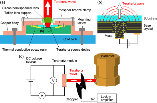
Figure 2. (a) Vertical cross-sectional view of the assembled terahertz source module. CW terahertz waves are emitted from the embedded source device to free space via a silicon hemispherical lens. (b) Enlarged schematic of the terahertz-emitting part encircled in (a). The solid lines represent the standing waves of the c-axis electric fields in the Bi-2212 mesa and base crystal associated with the Josephson plasma waves. (c) Schematic view of the experimental setup for I–V and terahertz-emission characterization.
Download figure:
Standard image High-resolution imageSome demonstrable advantages of our packaged modules are as follows: the fairly rigid and stable structure guarantees physical and chemical stability with good thermal contact. Therefore, the modules provide stable and reproducible emission characteristics with a high yield rate in contrast to those for stand-alone-type devices. We fabricated two packaged modules to examine the characteristic variation, and they exhibited reproducible current–voltage (I–V) and emission characteristics. The modules are as easy to use as conventional semiconducting LED light sources—researchers who are not experienced in using superconducting devices can easily operate them to generate desirable CW terahertz waves. All that is required is the application of a DC voltage to the device via the protruding electrode wires. The module can be mounted to any type of refrigerator and cryocooler system, depending on the intended use. The emitted waves are concentrated into a unidirectional beam by the collimating lens, which provides high efficiency in the use of the emitted electromagnetic energy. In addition, the use of cryogenic epoxy resins in the molding technique allows permanent use without damage from the oxygen and water vapor in air.
Figure 2(c) shows a schematic view of the experimental setup for measuring the I–V and emission characteristics. The emitting device was biased using the DC voltage source. During the I–V measurements, we also monitored the terahertz-emission power using a silicon composite bolometer with a 1 THz low-pass filter. For detection of the lock-in, the emitted waves were optically chopped at approximately 80 Hz. The output signal was amplified by a high-pass 200× preamplifier and recorded on a computer. The noise equivalent power of the detector was  . To measure the emission frequency, we used a home-built Fourier transform infrared (FT-IR) spectrometer consisting of a pair of flat lamellar mirrors (not shown here) [36]. The frequency resolution of the spectrometer is given by
  where
where  is the maximum differential displacement of the lamellar mirror and c is the speed of light. In the present setup,
  and, therefore,
  . The engineered source module was mounted on a helium-flow cryostat, and the bath temperature Tb was monitored using a thermometer attached to the cold bath. Since the terahertz wave is strongly absorbed by water vapor, it is preferable to use a dry nitrogen box between the cryostat and the bolometer.
3. Results and discussion
Figure 3(a) shows the four-terminal I–V characteristics measured at Tb = 20 (K). The red plot indicates the data when the emitting device was mounted on the module, as shown in figure 2(a). For comparison purposes, the black plot indicates the data when the device was mounted directly on the cold finger of the He-flow cryostat using silver paste as a glue in a conventional manner. When measuring the characterizations, we removed the capping resin used for molding the emitting device in order to separately determine the packaging and aging effects. Each I–V curve was obtained by a cyclic bias scan. The large hysteresis loop and the multiple branching structures in the low current regime exhibited behaviors typical of the intrinsic Josephson junction system. Since the gap voltage per junction was approximately 20 mV, the present stack with N = 720 should provide sufficient hysteresis with the maximum voltage of  (V). Nevertheless, the actual applicable voltage was compressed into the range of 2–3 V. This is attributed to the local temperature rise due to the enormous Joule heating, which gave rise to a decrease in the junction resistance. The strongly negative temperature coefficient of the c-axis resistivity (R) shown in the inset of figure 3(a) is thought to contribute to hot-spot formation in biased Bi-2212 mesas [24].

Figure 3. (a) Four-terminal I–V characteristics measured at Tb = 20 (K) for non-packaged (black) and packaged (red) conditions. Inset: temperature dependence of the c-axis resistivity. (b) Bolometer output as a function of voltage in the same scale as that of figure 3(a) for the packaged condition.
Download figure:
Standard image High-resolution imageFigure 3(b) shows the bolometer output as a function of voltage for the case of the packaged module. Intense terahertz emissions were observed in the low current regime indicated by the arrows in the figure. The module can generate a constant emission power with fluctuations less than a few percent as long as the bias point is fixed. The asymmetric behavior of the bolometer output under positive and negative voltage biases is attributed solely to randomness in the electrical switching during the I–V scans, which is a trivial issue in the intrinsic Josephson junction system. According to the sensitivity of the bolometer, the output signal of 1 mV corresponds to the emission power of 130 pW. By considering the directivity factor, the integral emission power is estimated to be in the order of microwatts. In the inner I–V branches where only some of stacked junctions were in the resistive state, the voltage per resistive junction corresponding to the Josephson frequency remained at almost a constant value. The emitted waves were linearly polarized and associated with the transverse magnetic cavity resonance [37, 38], where the E-field oscillated along the plane containing the c-axis and mesa width.
It is worth mentioning that, to the best of our knowledge, this is the first observation of terahertz radiation emitted from the back side of an underlying large Bi-2212 base crystal. The emission intensity was found to be comparable to that of the front side. It is speculated that the synchronization among adjacent multiple stacks of intrinsic junctions, which leads to significantly high-power radiation, is mediated by the Josephson plasma waves in the base crystal [15, 39]. More importantly, this observation indicates that the oscillating backside surface current associated with the excitation of the Josephson plasma throughout the entire crystal produces the intense radiation, as illustrated in figure 2(b). It is also likely that the emitted waves can penetrate through the base crystal without being screened by the excited quasiparticle current, since the high-Tc superconducting energy is supposed to be higher than the terahertz photon energy. Regardless, the option of backside radiation greatly expands the design possibilities of high-Tc terahertz sources. For example, we now expect to increase the emission intensity by positioning the reflector antenna at the back of the source.
The remarkable change in the hysteretic I–V loop shown in figure 3(a) provides a strong indication of the improved thermal contact due to the packaging. The thermal equilibrium condition in the resistive state is determined by a delicate balance between the Joule heating that is characterized by the I–V product and the thermal diffusion. Using our packaging technique, the excessive temperature rise is suppressed despite the larger I–V product that leads to more severe heating. We presume that this can be attributed to the use of the phosphor-bronze clamps, although epoxy molding is also an effective way to promote sufficient cooling. In fact, if we do not use the clamps, the obtained I–V characteristics and concomitant emission properties were quite sensitive to the amount of silver paste used for gluing.
Figure 4(a) shows the Tb dependence of the I–V characteristics, and Tb varied from 20 to 40 K at 5 K intervals. Based on the negative temperature coefficient of the c-axis superconducting energy gap, the I–V hysteresis decreased as Tb increased. In figure 4(b), the bolometer output at each Tb are plotted with an offset for ease of comparison. In these two panels, the obtained data is plotted with color-coded bolometer output. The maximum output power simply decreased with increasing Tb, and no appreciable emission was detected above Tb = 40 (K). This implies that the effective temperature of the biased mesa was close to Tc above Tb = 40 (K). We expect that this challenging self-heating problem will be solved by short-pulse techniques [40, 41].
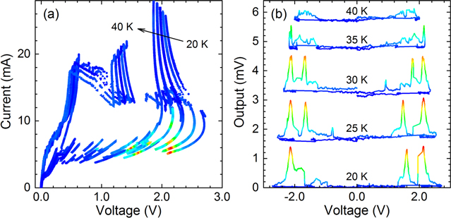
Figure 4. Tb-dependence of the (a) I–V characteristics, and (b) bolometer output. The data are plotted with the color-coded bolometer output.
Download figure:
Standard image High-resolution imageFigure 5 shows the emission spectra measured using the FT-IR spectroscopy. Here, these data were obtained from the packaged module that comes with a 70 μm wide emitting mesa. The distinct spectral peaks are observed at 0.505 THz (0.817 V), 0.522 THz (0.829 V), 0.553 THz (0.885 V), and 0.569 THz (0.894 V), respectively, where the voltage V is indicated on each spectrum. The solid lines represent Lorentzian peak functions with the best fits to the experimental data. The inset of figure 5 shows a linear relationship between V and the central frequency f. The error bars reflect the frequency resolution  of the spectrometer. Note that the spectral linewidth associated with the coherence of emitted waves is supposed to be much narrower than
  [16]. A dashed line in the inset represents the Josephson frequency fJ given by equation (1) with the experimental value of N = 660 determined by least-square fits. In this particular case, the f tunability of up to 13% was found by varying V. The tunable f range could be extended by examination of the Tb dependence [42] and the inner regions of the branched I–V characteristics [43].

Figure 5. FT-IR emission spectra for a 70 μm wide Bi-2212 mesa. The solid lines represent Lorentzian peak functions with the best fits to the experimental data. Inset: emission frequencies f as a function of V. The error bars reflect the frequency resolution of the spectrometer. A dashed line represents fJ given by equation (1).
Download figure:
Standard image High-resolution imageTo investigate the effect of the packaging on the thermal properties both quantitatively and qualitatively, we performed a numerical simulation using the COMSOL multiphysics simulation software package (www.comsol.com). By solving the standard equations of electrical and thermal conduction using the 3D finite element method, we can simulate a steady-state temperature distribution in an arbitrary geometry. In order to use realistic material parameters, the anisotropic electrical and thermal conductivities of Bi-2212 were extracted from the literature [44]. We also used realistic material parameters available from an extensive materials database, namely, the Network Database System for Thermophysical Property Data (http://tpds.db.aist.go.jp/tpds-web/). Those for STYCAST 1266 and APIEZON
 were found in their respective product data sheets. To make a distinction between the non-packaged and packaged modules, as indicated by the black and red plots in the I–V characteristics shown in figure 3(a), we assumed that the emitting device was attached to the copper body in one of two different ways. In the case of the non-packaged device, we used a 0.1 mm thick silver paste as a glue, whereas a small amount of vacuum grease was used in the packaged device.
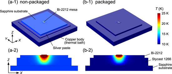
Figures 6(a-1) and (b-1) show 3D images of the simulated temperature distributions for the non-packaged and packaged cases, respectively. The two panels, namely figures 6(a-2) and (b-2), next to their corresponding 3D images show magnified 2D cross-sectional profiles in the X–Z cut plane. A color bar on the right-hand side indicates the temperature scale for each image. We set the bath temperature and bias voltage to 10 K and 2.1 V, respectively, which were extracted from the experimental data shown in figure 3(a). The boundary conditions were chosen to be  (zero flux) at the lateral and bottom sides of the copper body. For the non-packaged case, the thermal conductivity of silver paste at cryogenic temperatures was set to be 0.4 W m−1 K−1. Importantly, the effective area at the contact boundary between the sapphire substrate and the copper body had to be considered carefully—the real contact area, which is proportional to the heat flux, should have been considerably reduced due to the surface roughness of the silver paste. A surface probe using an atomic force microscope reveals that the actual contact area had decreased by nearly 90% of the apparent area. This was attributed to the relatively large diameter of the thermally conductive silver particles, typically 5 μm. Thus, we began by inserting an interfacial thermal resistance with 10% conductivity on the assumption that the heat transfer would be inhibited at the contact surface.
Figure 6. 3D images of the simulated temperature distributions for the (a-1) non-packaged, and (b-1) packaged emitting devices. (a-2) and (b-2) Magnified 2D cross-sectional temperature profiles in the X–Z cut plane extracted from the corresponding 3D images.
Download figure:
Standard image High-resolution image
After repeated simulations, we found that the increase in the effective area at the contact surface was key to the prevention of overheating. The homogeneous temperature distribution over the whole substrate was attributed to the extremely high thermal conductivity of the sapphire. Nevertheless, in the non-packaged case (see figures 6(a-1) and (a-2)), the substrate temperature increased globally by 4 K with respect to Tb due to the deteriorating thermal contact. Furthermore, the maximum local temperature at the emitting Bi-2212 mesa was 35.8 K for the non-packaged case, whereas it was 30.8 K for the packaged case. This intuitive result is consistent with the observed I–V characteristics—an emitting device that is attached with a better thermal contact exhibits a larger hysteresis in the I–V characteristics in accordance with the negative temperature coefficient of the c-axis resistivity. Further, terahertz-frequency electromagnetic simulations could provide valuable information about the maximum emission powers from the module after the great improvements in the thermal properties.
4. Conclusion
In conclusion, we engineered compactly-packaged CW terahertz source modules using intrinsic Josephson junction stacks in high-Tc Bi-2212 single crystals. The modules are small in size, i.e., fingertip size, and exhibit reproducible I–V and emission characteristics. The coherent and tunable terahertz waves can be emitted through the collimating lens, which is attached to the back side of the sapphire substrate. A numerical approach to simulate the 3D temperature distribution delivered consistent results. The modules are easy to use, and thus are suitable for practical use in many applications, especially in sensing, imaging, spectroscopy, etc.
Acknowledgments
The authors acknowledge T Kashiwagi, H Minami, K Kadowaki, and S Kawabata for valuable discussions. The Bi-2212 single crystals were provided by Y Nakagawa. Technical support from Kyoto Shisaku was greatly appreciated. This work was supported by KAKENHI (Grants No. 13J04811, No. 26790032, and No. 26286006), the University of Tsukuba Basic Research Support Program Type B, the Program to Disseminate the Tenure Tracking System at the University of Tsukuba, and the Project for University-Industry Cooperation Strengthening in Tsukuba. We would like to thank Editage (www.editage.jp) for English language editing.