

Abstract
We report on the enhancement of critical current density (Jc) and the unusual behaviour of its dependence on field orientation in YBa2Cu3O7−x (YBCO) nanostructured films by a combination of substrate decoration with Ag nano-dots, of the incorporation of BaZrO3 (BZO) nano-particles and nano-rods, and of multilayer architecture (a thin SrTiO3 layer separating two 1.5 μm-thick YBCO layers). SrTiO3 insulating layers were 15, 30 or 45 nm thick. The highest improvement of Jc in applied magnetic fields along the c-axis and smaller than 1 T occurs in the bi-layer with 30 nm-thick STO, but the influence of STO thickness is small. Our thick nanostructured films show significant improvement of Jc in the magnetic field along the ab-plane direction. The presence of BZO nano-rods, ab-plane defects and nano particles of BZO and Y2O3 was observed in transmission electron microscopy (TEM) images of the film. The peculiarities of artificial pinning centres revealed in the TEM images of the nanostructured films are used to explain an unusual split of the peak in the Jc dependence on the magnetic field along the ab-plane of YBCO. Effective pinning potentials in high magnetic fields have rather high values for such thick films.
Export citation and abstract BibTeX RIS
1. Introduction
Large-scale power applications of YBa2Cu3O7−x (YBCO) films processed as long-length coated superconductors depend on the development of low-cost methods for the preparation of thick films with a high critical current density (Jc) to obtain a high critical current per centimetre of width (Ic-w) [1]. For applications in moderate and high magnetic fields, high Jc and Ic-w values require a high density of defects (pinning centres, both natural and artificial) preventing motion of the magnetic flux induced by Lorentz force and thermal energy. The initial methods, such as substrate decoration [2–4] or deposition from composite targets, e.g. of YBCO with BaZrO3 (BZO) nanoinclusions [5] or with Gd2Ba4CuWOy [6], targeted one specific type of pinning centre. The improvement of Jc could be further increased by the proper choice of the architecture of the films, e.g. using a multilayer structure in which YBCO layers are separated by a thin insulating layer such as CeO2 [7]. Recent approaches have targeted several types of pinning centres by using double-doping, for example, with BZO and Y2O3 [8, 9], or Gd3TaO7 and YBa2NbO6 [10]. More recently, a large pinning force and matching effects were reported by the addition of mixed double perovskite Ba2Y(Nb/Ta)O6 which resulted in an unusual pinning landscape consisting of Ba2(Y/Gd)(Nb/Ta)O6 segmented nano-rods parallel to the c-axis, and (Y/Gd)2O3 plate-like nanoparticles parallel to the ab-plane [11] with a record irreversibility field of 11 T in the case of additions of Ba2YTaO6 and mixed Ba2YTaO6+Ba2YNbO6 nano-columnar inclusions [12].
We reported previously that the combination of the three methods—substrate decoration, BZO nano-inclusions and quasi-multilayer architecture—brings together the advantages of each approach, creating a very complex landscape of synergetic pinning centres. By combining substrate decoration with Ag nano-dots (which increased the critical current density, allowed the growth of thicker films without the usual drastic decrease in Jc and has been proven to promote the columnar growth of YBCO [13]) with BZO-doping, BZO nano-rods and nanoparticles act as effective pinning centres for the magnetic field in both directions: along the c-axis and in the ab-plane [14].
Over a decade ago, a radically different concept for high-Tc superconducting devices was proposed: coated conductor cylinders. This approach involves sequential deposition of YBCO and insulating layers onto a heated cylinder (a Ni or NiW alloy with bi-axially textured buffer layers; a cylinder with ion beam assisted deposition or inclined substrate deposition buffers). To produce a multilayer superconducting coil in situ, insulating layers are deposited by pulse laser deposition (PLD) followed by YBCO layers to electrically isolate one superconducting layer from another. These individual superconducting layers can also be 'cut' into trenches in situ using a laser beam, resulting in a multi-turn approach, and can be connected together in series or in parallel after the whole deposition and 'patterned' for a whole variety of power applications [15]. As for the insulating layers, CeO2, SrTiO3 (STO) and yttrium stabilized zirconia were tested [16], the best results being obtained for STO. Multi-layers of (120 nm STO/450 nm YBCO)n with n up to 6 (a total thickness of YBCO up to 2.7 μm) were successfully grown on buffered curved NiW RABiTS without any significant degradation in the crystalline structure and in the grain boundary orientation, thus proving the feasibility of this approach [17]. Those studies have been performed using pure YBCO targets. Moreover, field-dependent critical current studies on such structures have not been performed to the best of our knowledge.
The aim of this work was to grow and study the superconducting properties of such multilayers, this time with artificial pinning centres, and to investigate the influence of the STO on the pinning properties of YBCO layers, knowing that very thin (nm scale) layers have been shown to provide additional strong pinning along the ab-plane [18].
2. Experimental
Ag nano-dots were deposited on the STO substrate by PLD with the optimum conditions for deposition as reported in [13, 14]. Two BZO-doped YBCO layers and the separating STO nano-layer were grown at a temperature of 800 °C and a laser frequency of 4 Hz using a 4 wt.% BZO-doped YBCO target prepared by a citrate–gel method described in detail elsewhere [19], and a STO target, respectively. The thickness of the BZO-doped YBCO layers was 1.5 μm while the thickness of the insulating STO layer was 15 nm, 30 nm and 45 nm, respectively, with a total film thickness slightly above 3 μm. For comparison, a single-layer film of BZO-doped YBCO was fabricated under the same conditions as the bilayer films. The 3 μm-thick single layer film was of poor quality, so the comparison was made with a good quality 2 μm-thick single layer film.
The critical current density in the magnetic fields along the c-axis was determined from DC magnetisation loops of square 5 mm × 5 mm samples measured on a quantum design magnetic properties measurement system (MPMS-XL) in a DC field up to 4.5 T, using a critical state model, as in [13] and [14]. The critical temperature (Tc) was measured on an MPMS-XL by recording the temperature dependence of the AC susceptibility in a small excitation field of 0.05 Oe. In magnetic fields of arbitrary orientation, Jc was determined from the angle-dependent transport measurement using a voltage criterion of 1 μV cm−1 on 550 μm long and 10 μm wide micro-bridges produced by conventional photolithography and chemical etching. The angle-dependent measurements were conducted on a quantum design physical properties measurement system (PPMS). Due to the limited access to PPMS, transport measurements were performed for one bi-layer sample only, and the results are compared with other types of YBCO films, as stated above. Using the same equipment with a different set-up, pinning potentials were estimated from frequency-dependent AC susceptibility measurements using a technique and data analysis as described in detail elsewhere [20]. Such AC susceptibility measurements are currently on-going on other bi- and multi-layers, and the results will be reported elsewhere. The micro- and nanostructure of the samples was analysed by scanning electron microscopy (JEOL 7000) and transmission electron microscopy (TEM, Technai F20 operated at 200 kV). The cross-sectional TEM samples were prepared by focused-ion-beam milling on an FEI Quanta 3D FEG.
3. Results and discussion
The superconducting properties of the bilayers were first examined by AC susceptibility measurements during slow temperature scans of 0.2 K min−1. All the films show quite a sharp transition at a high Tc of 88.5–89.5 K, as can be seen in figure 1, where S15, S30 and S45 indicate the STO thickness of 15, 30 and 45 nm. S0 denotes the single-layer of BZO-doped YBCO film (2 μm-thick) deposited on a Ag-decorated STO substrate. The critical current density (Jc) for the bilayer films with different thicknesses of an insulating STO layer is shown in figure 2 in comparison with the Jc of S0. Jc was measured at a temperature of 65 K (temperature of interest for superconducting devices in pumped nitrogen) and applied fields up to 4.5 T perpendicular to the film surface, and at 77.3 K in fields up to 3.5 T. At 77.3 K, the Jcs of all the 3 μm-thick bi-layers are slightly smaller than that of the 2 μm-thick single layer film. At 65 K, the bilayer film with a thickness of the STO layer of 30 nm has the highest Jc in a self-field of about 3.86 MA cm−2, while the Jcs of the bilayer films with an STO layer of 15 and 45 nm are of 2.86 and 3.53 MA cm−2, respectively. The self-field Jc of all bilayer films at this temperature is higher than that of the single-layer BZO-doped YBCO film deposited on the Ag-decorated STO substrate, which is about 2.67 MA cm−2. The Jc of the bilayer films continues to be higher than that of the single layer film in fields up to 1 T for S30, up to 0.5 T for S45 and up to 0.1 T for S15. It can be seen that the highest Jc is for the film with a 30 nm-thick STO layer, but the reason for this is unclear. In high applied fields, for example at 4 T, the Jc of the single-layer film is the same as in the bilayer films with a thickness of the STO layer of 30 and 45 nm (≈0.3 MA cm−2). Some of the values of the critical current density for the samples discussed above are shown in table 1. The differences in Jc are rather small, perhaps even in the limit of variability between subsequent depositions, so we can conclude that in an applied field perpendicular to the film surface, no significant improvement or significant degradation in Jc for bilayer films is observed in comparison with the Jc of single-layer film.
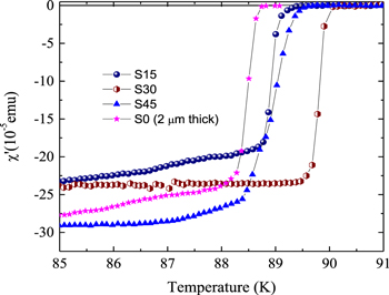
Figure 1. Temperature dependence of the in-phase susceptibility of bilayers composed of two 1.5 μm BZO-doped YBCO films separated by STO layers with a thickness of 15 nm (S15), 30 nm (S30), and 45 nm (S45), and of a 2 mm-thick single-layer BZO-doped YBCO film (S0) on a Ag-decorated STO substrate.
Download figure:
Standard image High-resolution image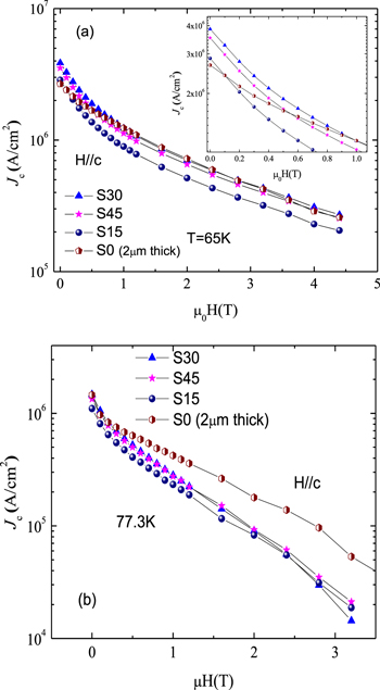
Figure 2. Field dependence of the critical current densities of bilayers composed of 1.5 μm BZO-doped YBCO films separated by an STO layer with a thickness of 15 nm (S15, spheres), 30 nm (S30, triangles), and 45 nm (S45, stars) in comparison with Jc of a single-layer BZO-doped YBCO film (S0) on a Ag-decorated STO substrate with the same thickness, at a temperature of 65 K and applied fields parallel to the c-axis of YBCO. The inset shows a magnified area of figure 1 in applied fields between 0 and 1 T.
Download figure:
Standard image High-resolution imageTable 1. Critical current densities (in MA cm−2) at 65 K for the four samples in applied fields between 0 and 4 T parallel to the c-axis.
| Field (T) | |||||||
|---|---|---|---|---|---|---|---|
| Sample | 0 | 0.1 | 0.2 | 0.5 | 1 | 2 | 4 |
| S0 | 2.67 | 2.4 | 2.15 | 1.68 | 1.23 | 0.72 | 0.29 |
| S15 | 2.9 | 2.4 | 2 | 1.37 | 0.9 | 0.5 | 0.23 |
| S30 | 3.86 | 3.27 | 2.77 | 1.89 | 1.23 | 0.7 | 0.31 |
| S45 | 3.53 | 2.97 | 2.51 | 1.7 | 1.12 | 0.65 | 0.29 |
In applied fields parallel to the film surface, the Jc of bilayer films obtained by transport measurement (1 μV cm−1 criterion) shows significant improvement in comparison with single-layer films, even when the single-layer films are thinner than the bilayer films, as shown in figure 3. This figure compares the Jc of the 3 μm bilayer film with the 45 nm STO layer with the 2 μm single-layer film on a bare STO substrate, and a 2 μm single-layer film on the Ag-decorated substrate in applied fields up to 6 T and a temperature of 77.3 K. It is well known that for the same composition and growth conditions, the Jc of a 3 μm film is smaller than that of a 2 μm film, the critical current density decreasing with increasing thickness above an optimum one of several hundred nm [1], so we can safely conclude that the STO layer promotes the improvement of Jc for fields parallel to the ab-plane.

Figure 3. Field dependence of critical current density of 3 μm bilayer film (magenta stars), 2 μm single layer BZO-doped YBCO film on a bare STO substrate (blue squares) and 2 μm single-layer BZO-doped YBCO film deposited on a Ag-decorated STO substrate (white-brown hexagons) in an applied field parallel to the ab-plane of YBCO at 77.3 K.
Download figure:
Standard image High-resolution imageIn a self-field, the Jc of the bilayer film (pink stars) shows a 100% increase in comparison with the Jc of the single-layer film (blue squares). In an applied field of 6 T, the Jc of the bilayer film (70 kA cm−2) is 43% higher than that of single-layer film on a bare substrate with a Jc of 49 kA cm−2, while the Jc of the film on a Ag-decorated substrate (white-brown hexagons) is in-between with the value of 59 kA cm−2. It is obvious that the STO layer separating the two BZO-doped YBCO layers helps to increase Jc at 77 K both in a self-field, and in fields up to 6 T parallel to the ab-plane.
It has been previously reported [7] that, in applied fields below 2.5 T, Jc in BZO-doped YBCO films is larger for magnetic fields applied along the c-axis of YBCO, with a maximum of  where
where  is the critical current density for the magnetic field along the c-axis and
  is the critical current density for the in-plane magnetic field. The same property can be seen in the bilayer film with a 45 nm STO layer as shown by the angular dependence of Jc at a temperature of 77.3 K presented in figure 4. In an applied field of 0.6 T, the
  of the bilayer film at 0, 180 and 360° is twice the
  at 90 and 270°. The
  ratio reduces to nearly 1 in an applied field of 2.5 T, and decreases further with an increase of the applied field, returning, for high fields, to the 'normal' situation in which
  where
where  is the YBCO anisotropy factor.
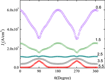
Figure 4. Angular dependence of the critical current density of the bilayer film at 77.3 K. The value of the applied magnetic fields is shown on the right hand side of each curve.
Download figure:
Standard image High-resolution imageIn an applied field of 2.5 T, the Jc of all three samples—bilayer film, a single layer on bare STO substrate and a single layer on a Ag-decorated STO substrate—show a low anisotropy of Jc with  , as shown in figure 5. Again, the Jc for a field along the ab-plane of the 3 μm bilayer film (blue squares) is higher than that of a 2 μm single-layer film on a Ag-decorated STO substrate (red circles) and of the single-layer film on bare substrate (black triangles). The Jc for a field along the c-axis of the single-layer film on a Ag-decorated substrate, however, is higher than that of the bilayer film due to the thickness difference, as discussed above. As shown in figure 5, the Jc for fields along the c-axis of the bilayer is almost the same as in the single-layer film on the decorated substrate in an applied field of 2.5 T.

Figure 5. Angular dependence of critical current density in an applied field of 2.5 T and temperature of 77.3 K for a 3 μm bilayer (blue squares), 2 μm single-layer on a Ag-decorated substrate (red circles) and 2 μm single-layer on bare substrate (dark triangles). All films show low anisotropy of critical current density, close to 1.
Download figure:
Standard image High-resolution imageIn bilayers, for the field directions close to the ab-plane, the peaks of Jc at 90° and 270° are split into two peaks, as can be seen in figure 5. The cross-sectional TEM image of the bilayer film shown in figure 6 reveals the presence of fragments of planar defects parallel to the STO layer. If the average length of these fragments, schematically shown in figure 7 by thick black lines, is L, and the average distance between them along the c-axis is l, then the optimal angle φ at which pinning is at its strongest, and segmented vortices fit best to the planar defects, is given by relation:

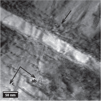
Figure 6. Bright field cross-section TEM image of bilayer film around an STO insulating layer, the c- and ab-axis of the film are marked by arrows.
Download figure:
Standard image High-resolution image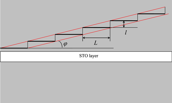
Figure 7. Schematic representation of the pinning of vortices with their average direction along the red lines. The optimum pinning is achieved when the slope of the vortex line is equal to the angle φ defined by the average length L of the planar segments (thick black lines) and average distance between them l along the c-axis.
Download figure:
Standard image High-resolution imageThe TEM image in figure 6 allows for very rough estimates of L as 150 nm and l as 50 nm, which results in φ of approximately 18°. Of course, just from one TEM image, statistical analysis of the observed defects along the ab-plane is very difficult to perform, so the values selected for L and l are just for qualitative analysis. The resulting value for φ is close to that observed in figure 4 with positions of split maxima situated at 90° ± φ and 270° ± φ.
The in-plane defects are only observed in the areas near the STO substrate and close to the STO insulating layer, while the c-axis columns of BZO appear in the middle of BZO-doped YBCO layers, as shown in figure 8. The combination of the ab-plane and the c-axis defects act as active pinning sites maintaining high Jc, not only in the direction of applied magnetic fields parallel to the c-axis, but also for fields in the ab-plane, and this very peculiar pinning landscape is responsible for the split of the ab-plane peak in the Jc(θ). This split due to pinning centres with different orientations resembles, somewhat, the split in the field-dependence of the pinning force due to the presence of different types of pinning centres [21]. Another origin of pinning in the BZO-doped YBCO films is in the presence of Y2O3 nano-particles frequently observed in the bilayer sample and shown in figure 9. Although in [8], Y2O3 nano-particles were added to the BZO-doped YBCO target to create more effective pinning, in our bilayer films, the presence of Y2O3 nano-islands occurs naturally during film deposition.

Figure 8. TEM image of extended BZO nano-rods in the YBCO far from the STO layer.
Download figure:
Standard image High-resolution image
Figure 9. TEM image of an Y2O3 nano-particle in the matrix of YBCO.
Download figure:
Standard image High-resolution imageThe critical current density can also be calculated from the AC susceptibility while a DC field is applied to the sample. Brandt [22] showed that, for superconducting thin films, the position h* of the maximum in the AC-field dependence of the out-of-phase susceptibility χ''(hac) is related to the critical current density by the equation

where d is the film thickness and α is a constant between 0.8 and 0.9 that depends slightly on the geometry (disc, square, rectangle). An example of such frequency-dependent χ''(hac) measured curves is shown in figure 10 for a bi-layer with a 30 nm-thick STO nanolayer at 77.3 K and in a 7 T DC field. From the frequency (time) dependence of the critical current density presented in figure 11, one can estimate the pinning potential, as shown in detail in [20]. In brief, our data are very well described by a straight line in a double logarithmic plot in figure 11:

where f0 is a macroscopic attempt frequency of about 106 Hz. The effective pinning potential, U0, can be related [20] to the slope b in equation (3) of our experimental data:

Using equation (4) and the data in figure 11, we estimated the effective pinning potential of the synergetic pinning centres in this film at 77.3 K. The values (in K, kB = 1) are 389 K (in 5 T), 271 K (in 6 T) and 176 K (in 7 T). It is worth mentioning that, due to limitations in the AC-field amplitude (hence, in the probing current), the experimental window in which such a technique can be used is limited to high fields in thicker films, as in our case.
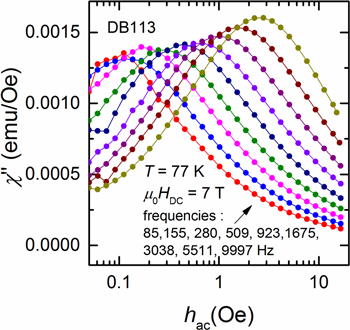
Figure 10. Dependence of the out-of-phase susceptibility of the bi-layer film with 15 nm STO on the amplitude of the AC field for various frequencies (indicated in the image), in 7 T and at 77.3 K.
Download figure:
Standard image High-resolution image
Figure 11. Frequency-dependence of the critical current density of the same bi-layer film at 77.3 K in fields of 5, 6, and 7 T.
Download figure:
Standard image High-resolution image
In conclusion, the introduction of 15–40 nm thick STO films between YBCO layers does not degrade the critical current density. The combination of the three methods (substrate decoration, multilayers, BZO doping) is effective in increasing the Jc of the film for magnetic fields oriented in both the c-axis and the ab-plane. It appears that a 30 nm STO layer gave the best results, for reasons yet unclear, but the differences in Jc for fields along the c-axis is rather small. A significant increase of Jc for fields along the ab-plane of the bilayer film has been achieved. The presence of the fragments of ab-plane defects explains the split of the Jc peak in its dependence on magnetic field orientation close to the ab-plane of YBCO. In a perpendicular configuration, frequency-dependent AC susceptibility measurements allowed estimations of quite high effective pinning potentials in high magnetic fields.
Acknowledgments
This work has been supported by the COST Action MP 1201 'Nanoscale SuperConductivity: Novel Functionalities through Optimized Confinement of Condensate and Fields' and by the Romanian Ministry of National Education and Research through the Core Programme PN16-480102 'Synthesis and characterisation of nanostructured materials, thin films and heterostructures'; through PCCA 138/2012; and through the POC Project P_37_697 (28/01.09.2016) 'Boron- and rare-earths-based advanced functional materials'. VSD acknowledges financial support from the Vietnam National Foundation for Science and Technology Development (NAFOSTED) under grant number 103.99-2015.81.