

Abstract
The advancement of ternary GaAsSb mismatched alloy system toward the Sb-rich corner of the phase diagram in the nanowire (NW) configuration on silicon remains a challenge. A large lattice mismatch between the silicon substrate and GaAsSb with an Sb-rich composition, along with the low supersaturation and low solubility of Sb in the Ga droplet in the vapor–liquid–solid growth mechanism, causes significant issues during Ga-assisted molecular beam epitaxial growth of these NWs. In this work, we have carried out a systematic study of Sb-rich GaAs1–xSbx NWs grown on Si (111) using variations of the Ga, As, and Sb beam equivalent pressures (BEP) to minimize undesirable parasitic growth and achieve photoemission up to 1.7 μm. Ga-assisted molecular beam epitaxy is the enabling growth technology for the growth of these self-catalyzed GaAs1–xSbx (x > 0.8) NWs. The use of a dual substrate temperature approach along with low As background pressure and a low Ga BEP were found to be the key growth components in achieving a well-faceted NW morphology with a low parasitic layer on the substrate. Energy-dispersive x-ray spectroscopy analysis confirms uniform compositional homogeneity along the NWs, while selected-area electron diffraction patterns in the transmission electron microscope revealed a zinc-blende crystal structure. A peak μ-photoluminescence emission of 1680 nm with a narrow FWHM was obtained at 4 K. Raman spectra at room temperature exhibit only GaSb related LO and TO modes, which attest to the high quality of the NWs grown. This is a promising approach due to the broad scope of applicability to grow other mismatched alloy material systems in a NW configuration.
Export citation and abstract BibTeX RIS
1. Introduction
Nanowires (NWs) are ideally suited as building blocks for applications in next generation devices such as single photon detectors [1], low power logic operations [2], nanophotonic integrated circuits [3], and infrared photodetectors [4]. GaAsSb is a well-known material system for growing NW structures to achieve wide bandgap tunability from 900 to 1700 nm. However, most of the reports are limited to the lower end of the wavelength region due to the challenges in growth of the NWs in the Sb-rich regime of the phase diagram, i.e., GaAs1–xSbx (x > 0.5) [5–9]. The technical barrier to the growth of these Sb-rich compositions arises in this composition regime (x > 0.5) due to higher strain caused by the larger lattice mismatch between the ternary alloy and Si substrate [10, 11], as well as the differences in their thermal expansion coefficients. This becomes more pronounced in the NW growths due to the vapor–liquid–solid (VLS) mechanism, which is a near-equilibrium technique, being the predominant growth mechanism. Additionally, in the self-assisted molecular beam epitaxial growth where the growth is initiated by supersaturation of the catalyst droplet by the group V species, the low solubility [12] and low supersaturation of Sb in Ga and the reduction in droplet contact angle with Sb incorporation in the droplet tend to inhibit vertical growth of GaAsSb NWs [13], and likely cause droplet instability during growth initiation leading to failure of vertical growth. These issues translate to a narrow window of Sb/Ga ratio for growth; furthermore, in this mixed As–Sb material system, As–Sb exchange dynamics [9, 11] make the growth control more complex and stringent.
In this work, our initial investigation was a systematic study of variation in the growth temperature and Sb/Ga ratio with particular emphasis on their impact on the Sb incorporation, extent of parasitic growth and NW density. The initial results led to subsequent investigation of a two-temperature growth approach, where one takes advantage of higher Sb incorporation at lower growth temperature. A dual temperature method has also been previously employed to grow GaAsSb (lower growth temperature) on GaAs stems (higher growth temperature), since higher antimony incorporation in the ternary alloy requires lower temperature and reduced growth rate compared to GaAs NW growth [4, 11, 14, 15]. However, parasitic growth dominates at lower temperatures for Sb-rich growth and is accompanied with deteriorated structural and optical properties of the NWs. Variation of the effective Sb/Ga ratio with NW density further increases the complexities in the growth of Sb-rich NWs [9, 16, 17].
The unsuccessful implementation of a two-temperature approach prompted us to explore Ga flux variation to mitigate the parasitic issues and quality of the NWs. The literature on Ga droplet epitaxy and NW growth with emphasis on the role of Ga as a catalyst has been investigated over a wide range of Ga partial pressures on a variety of substrates [18–23]. However, the full scope of the Ga beam equivalent pressure (BEP) on the Sb incorporation has not yet been explored experimentally. In this study, we evaluate the role of Ga on the Sb incorporation in self-catalyzed NW growth on Si (111) and associated phenomena that are relevant to this highly mismatched Sb-rich GaAsSb NW-Si substrate combination. Direct impingement of the As vapor flux using an As valved cracker and use of a background As pressure (with the As valve open and the shutter closed) have also been examined to achieve additional insight into the effect of very low As flux on morphology and optical properties of NWs. These studies led to the successful growth of Sb-rich GaAsSb NWs with good compositional homogeneity, density, excellent optical and microstructural quality using a dual-temperature approach with low Ga BEP strategy and low background As4 flux component. The promising results of this work potentially pave the way for the direct integration of III-Sb NWs on Si substrates over the entire composition range of the GaAsSb phase diagram.
2. Experimental details
The growth of GaAs1–xSbx (x > 0.8) was carried out on chemically etched (piranha/HF) p-type Si (111) substrates in a solid-source EPI 930 molecular beam epitaxy (MBE) system with valved As and Sb crackers. The details of the Si substrate preparation are provided in Kasanaboina et al [24]. The BEP of the constituent flux elements used are provided in the results and discussion section.
Scanning electron microscope (SEM) images were acquired using a high-resolution Carl Zeiss Auriga-BU FIB field emission scanning electron microscope. Scanning transmission electron microscopy (STEM)—energy-dispersive x-ray spectroscopy (EDS) was used to extract a detailed compositional profile of the NW samples, which was performed on a probe aberration-corrected FEI Titan G2 system operated at 200 kV. Micro-photoluminescence (μ-PL) measurements were conducted in a low-vibration closed-cycle optical cryostat from Montana Cryostation with a He–Ne (λ = 633 nm) laser for excitation. The laser power was varied for excitation power dependent measurements using a neutral density filter. The PL signal from the sample was then dispersed through a 0.32 m double grating monochromator with liquid nitrogen cooled InGaAs detector for detection using conventional lock-in techniques. Raman spectroscopy was carried out at ambient temperature using a Horiba Jobin Vyon confocal Raman microscope with a He–Ne (λ = 633 nm) laser.
3. Results and discussion
Initial investigation on using higher Ga BEP of 1.2 × 10⁻⁷ Torr for growth of Sb-rich NWs on a stem is presented. A suitable substrate temperature is then identified for high Sb incorporation with good surface morphology. For the growth of GaAsSb NWs on Si (111) with minimal stem a lower Ga BEP of 2 × 10⁻⁸ Torr is employed. This would also impact the parasitic layer growth, as it occurs via the vapor–solid (VS) mechanism and is limited by the group III, i.e. Ga, flux. Any decrease in group III flux therefore would then lead to less material deposition on the substrate. In the lower Ga BEP regime, we have experimented with low direct As BEP as well as background As pressure. The NWs thus grown using optimized results of lower Ga and As BEPs were then examined further, for structural and optical characteristics and are discussed in detail in respective sections.
3.1. NW growth results
3.1.1. GaAs1–xSbx on GaAs0.9Sb0.1 stem using a high Ga BEP of 1.2 × 10⁻⁷ Torr
A two-step growth temperature sequence for the growth of high Sb content NW was examined with As rich GaAs1–xSbx(x = 0.10) stems grown at 620 °C followed by GaAs1–xSbx (0.1 < x < 0.64) segments grown at lower substrate temperatures. The latter will henceforth be referred as the Sb-rich segment. For the stem growth, a higher V/III ratio of 20 was employed while it was ∼7 for the Sb-rich segment. As Sb incorporation increases with a reduction of the growth temperature [11], growth temperature variation between 580 °C and 520 °C was examined. Figure 1(a) for 580 °C reveals an inability for growth of a Sb-rich segment on top of the stem due to increased desorption of Sb at higher temperatures. By lowering the growth temperature to 550 °C, a distinct Sb-rich segment can be seen in figure 1(b). The morphology was found to change from a shorter segment with a large droplet on top to a more elongated NW with the droplet almost consumed, as the substrate temperature decreases from 550 °C to 520 °C as seen in figure 1(c). Both of them exhibit hexagonal facets. At lower temperature, the higher Sb incorporation leads to consumption of the droplet. The Sb at% increased from ∼36% to ∼64% for temperature reduction from 550 °C to 520 °C with a concomitant increase in 2D parasitic growth on the substrate, which is attributed to excess Sb forming a thicker 2D layer with available Ga. Further, longer NW segments with higher Sb content require longer growth duration due to the slow growth rate. Therefore, this undesirable parasitic layer is unavoidable for the given range of Ga flux (∼10−7 Torr BEP) and temperatures used for the growth of high Sb content segments.
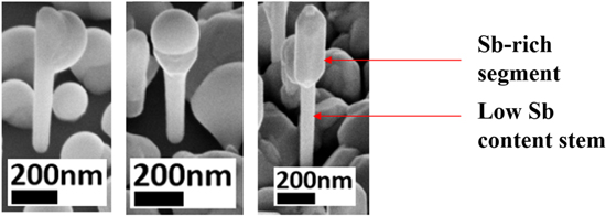
Figure 1. SEM images of GaAs1–xSbx (0.1 < x < 0.64) on GaAsSb stems on Si (111) substrate at (a) 580 °C, (b) 550 °C, and (c) 520 °C.
Download figure:
Standard image High-resolution imageTo suppress the undesirable 2D parasitic layer, a lower Ga BEP of 2 × 10⁻⁸ Torr was investigated, which is below the equilibrium vapor pressure of bulk Ga at 620 °C. All the results described in the following section refer to the NWs grown under the optimized Ga BEP of 2 × 10⁻⁸ Torr with a substrate temperature of 550 °C.
3.1.2. GaAs1–xSbx without stem on Si using low Ga BEP of 2 × 10⁻⁸ Torr
- (i)Growth under controlled As BEP
The Ga BEP of 2 × 10⁻⁸ Torr and an As/Ga ratio of 2 yielded a highly uniform growth of NWs over the entire substrate as seen in figure 2(a). The Sb incorporation for these NWs was ∼35 at% as confirmed from SEM-EDX spectroscopy. The diameter of the NWs increases from 180 nm for Sb/Ga ratio of 6–250 nm for a Sb/Ga ratio of 9, as shown in figure 2(c), with Sb incorporation varying in the range from 35 to 40 at%. Both the parasitic and stem growths were suppressed and very high density of NWs in the range of ∼4 μm–2 was achieved. To increase the incorporation of Sb, the As/Ga ratio was reduced to 1, and the density of bent NWs was observed to increase with an Sb/Ga ratio of 8 as shown in SEM image figure 2(b). For these NWs, PL spectra with PL emission extending to ∼1680 nm, which corresponds to an Sb incorporation of x = 0.8, was achieved. This is discussed later in the PL section. The increase in NWs failing to grow vertically is most likely attributed to a reduction in the contact angle as well as in the surface energy of the droplet with a higher Sb flux [13, 25]. For NWs grown using an As/Ga BEP ratio of 1, an Sb effect dominates due to Sb-rich conditions and thus the reduction in As BEP did not have any significant effect on the diameter of the NWs.
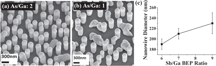
Figure 2. High-density growth of GaAs1–xSbx NWs using As/Ga BEP ratio of (a) 2 and (b) 1. (c) Nanowire diameter variation with Sb/Ga BEP ratio.
Download figure:
Standard image High-resolution imageThe length of NWs is restricted to ∼500 nm. This is explicable as higher NW density leads to lowering of the effective local supersaturation due to the reduction in local V/III ratio. When combined with a limited supply of material available in the given lower flux regime, this causes the observed truncation of the vertical growth. This is consistent with the observation of pitch dependent NW length reported for III–V Sb NW arrays [9, 16, 17]. For patterned growth of NWs, it has been established that the effective Sb/Ga ratio is directly influenced by the distance between the NWs [9, 17]. It has also been suggested in the literature that the effect of density on NW length is more pronounced if the diffusion length of atoms is higher [9, 26]. These observations are relevant to our Sb-rich unpatterned growth since difference in NW lengths can be explained in terms of the NW density. Hence, in the GaAsSb growth, as Sb adatoms have much higher surface diffusion than As adatoms [9], a high NW density severely limits the axial growth rate. Relatively longer NWs are obtained for low density growth when As is used as background pressure, as demonstrated in the next section. Thus, with increasing Sb, the low supersaturation as well as density-dependent material competition and their effects on the effective Sb/Ga ratio are the factors controlling the axial growth rate.
A schematic of the NW growth is shown in figure 3 for the two-temperature growth approach corresponding to the two different Ga BEP values discussed above. High-temperature growth of GaAs0.9Sb0.1 at 620 °C is followed by growth of Sb-rich GaAs1–xSbx NWs at a lower temperature of 550 °C. For a constant Ga BEP of 2 × 10⁻⁸ Torr, this strategy led to the growth of an Sb-rich segment with no visible low Sb composition stem growth. This is attributed to the use of low Ga BEP of 2 × 10⁻⁸ Torr, which is lower than its vapor pressure at 620 °C.
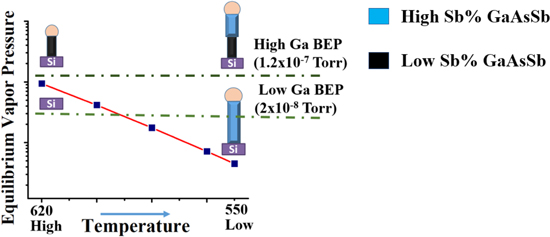
Figure 3. Schematic shows growth process for high Ga and low Ga BEPs.
Download figure:
Standard image High-resolution imageSince low Ga BEP was found to successfully mitigate the parasitic growth problem, in the following section we discuss the effects of other growth parameter variations, namely the background As pressure and Sb/Ga BEP ratio to further improve Sb incorporation in the NWs with particular emphasis on achieving longer lengths and good NW density.
- (i)Growth under background As BEP
Using a low Ga BEP of 2 × 10⁻⁸ Torr, the effects of varying the Sb/Ga BEP ratio on the NW morphology, density, and length were investigated. A background As pressure was used for the growth of GaAs1–xSbx NWs on Si (111). An arsenic flow as a background pressure has been used to grow GaAs1–xSbx NWs on a GaAs stem recently with Sb incorporation up to x = 0.93 [11]. In this section, the role of As background pressure to maximize the Sb incorporation in the GaAsSb NWs grown on Si has been explored. A background As BEP of 2 × 10⁻⁸ Torr has been used, which was obtained under closed As shutter condition with the As valve left open. The NWs for a BEP ratio of 2 and 4 show similar morphology: clear hexagonal faceting with slightly inverse tapering as seen from the SEM image in figures 4(a) and (b). These NWs also exhibit an Sb-deficient region under the droplet as confirmed from TEM analysis discussed later.

Figure 4. SEM images of GaAs1–xSbx for Sb/Ga BEP ratio of (a) 2, (b) 4, (c) 6 and (d) 10.
Download figure:
Standard image High-resolution imageFor an Sb/Ga BEP ratio of 6, GaAs0.2Sb0.8 NWs with average length ∼1 μm and diameter ranging from ∼150 to 180 nm, were observed as seen in the SEM image figure 4(c). Growth tends to cease as the higher group V flux consumes the Ga droplet. Although the droplets are mostly consumed in figure 4(c), some NWs in this sample exhibited partially consumed droplet at the top of NW, thus confirming a VLS growth mode. For an Sb/Ga BEP ratio of 10, as seen in figure 4(d), only few NWs were observed with concomitant increase in the two-dimensional growth.
The compositional analysis was done using STEM-EDS and SEM-EDX. The combined results from EDS compositional analysis and SEM images show that morphology and Sb content are highly sensitive to a Sb/Ga ratio change. Figure 5(a) illustrates the variation in Sb composition and PL emission wavelength with Sb/Ga BEP ratio. For ratios of 2 and 4, Sb compositions did not vary significantly and were found to be 35% and 40%, respectively, whereas the Sb incorporation increased to 80% for ratios of 6 and 10. This somewhat large transition from 40 to 80 at% is speculated to arise from the existence of the miscibility gap for GaAsSb composition in this range. It is to be noted that PL variations are consistent with Sb at% variations.

Figure 5. Effect of Sb/Ga ratio on (a) 4 K PL and incorporation of Sb at% and (b) variation of NW diameter, density and length in GaAs1–xSbx NWs.
Download figure:
Standard image High-resolution imageFor NWs grown under an As background pressure, a relatively lower density of NWs was obtained in comparison with those grown under direct As flux. Consequently, relatively longer NWs were obtained for these growths due to the increased distance between NWs, consistent with our earlier discussion and other findings in the literature [16, 17]. Figure 5(b) illustrates how the NW length, diameter, and density depend on the Sb/Ga BEP ratio. NWs with similar morphological features and aspect ratios were chosen for statistical analysis. The NW density up to an Sb/Ga ratio of 6 is ∼0.4–0.5 μm–2 but decreases to ∼0.2 μm–2 with further increase in BEP ratio to 10.
The results for high Sb content NWs indicate that there exists a narrow window of Sb/Ga ratio that provides a reasonable yield of NWs. Thus, the background As has a significant impact on Sb incorporation and also yields longer NWs of superior structural quality, as confirmed by PL and TEM results that are discussed later. The combined analysis of figures 5(a) and (b) indicates (Sb)-limited supersaturation typical of axial NW growth by the VLS mechanism. Hence, all data presented in the TEM section will correspond to NWs grown under As background pressure with an Sb/Ga ratio of 6 as these parameters represent optimal growth conditions corresponding to creation of long, faceted NWs of fairly good density and maximum Sb incorporation.
3.2. Characterization results for optimized NWs
3.2.1. TEM observation of crystal phase of NWs
NWs grown on Si without a stem (using low Ga flux) exhibit a distinct faceted morphology, which is a common signature of III–V-Sb NWs. Figure 6(a) shows a TEM image of the bottom region of the NW. The initial NW growth shows multi-faceted sidewall morphology near the NW-substrate interface, with evolving facets with increasing NW diameter until a hexagonal morphology and stable droplet diameter is attained. After this point, the developed hexagonal faceted morphology grows steadily until the droplets are consumed. Figure 6(b) shows the selected-area electron diffraction pattern along the ![$[1\bar{1}\bar{1}]$](https://content.cld.iop.org/journals/0268-1242/33/12/125007/revision2/sstaae7b8ieqn1.gif) zone axis which reveals excellent crystal quality with pure zinc blende crystal structure in the NW with no evidence of planar defects.
zone axis which reveals excellent crystal quality with pure zinc blende crystal structure in the NW with no evidence of planar defects.
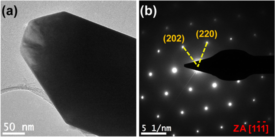
Figure 6. (a) TEM image of the bottom segment of a typical GaAs0.2Sb0.8 NW. (b) SAED pattern along ![$[1\bar{1}\bar{1}]$](https://content.cld.iop.org/journals/0268-1242/33/12/125007/revision2/sstaae7b8ieqn2.gif) zone-axis shows ZB crystal structure.
zone-axis shows ZB crystal structure.
Download figure:
Standard image High-resolution imageDepending on which growth mechanism dominates (VLS or VS), and depending on thermodynamic stability upon nucleation, either of the (110) and (112) facets can prevail in the III–V system [25]. The angle between the observed facets in our case is 30° which is the difference between (110) and (112) facets [27]. The base diameter of the NWs is smaller due to strain at the NW-substrate interface as expected in lattice mismatched NW growth [28]. The stress in the NWs is relaxed by the formation of additional facets in the crystal, here a more regular hexagonal faceting. The determination of orientations of these facets warrants further study to understand strain relaxation at the NW-substrate interface and improve integration of NWs on lattice-mismatched substrates.
The compositional homogeneity throughout the NW in the axial direction was confirmed using elemental mapping as represented in the figures 7(a) and (b) for NW without the droplet and with the droplet, respectively. Figure 7(a) demonstrates the EDS compositional maps for GaAs1–xSbx NWs without a droplet on top and having compositional homogeneity. The NWs with an Sb/Ga ratio of 2 (see figure 7(b)) show an Sb-deficient/As-rich region below the Ga droplet, which is consistent with the reports of Li et al [11].
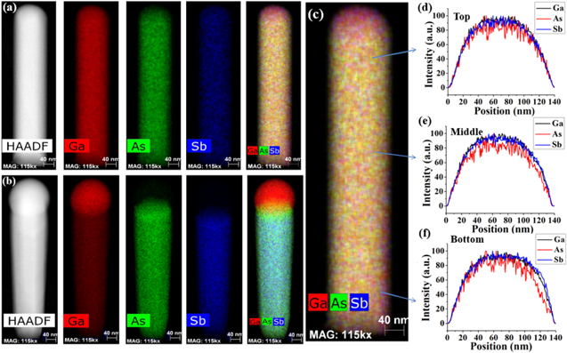
Figure 7. (a) EDS compositional mapping of GaAs1–xSbx NW with Sb/Ga BEP ratio = 6 and (b) Sb/Ga BEP ratio = 2 (c) STEM-EDS compositional map (d)–(f) EDS line scan showing compositional profile of NWs for Sb/Ga = 6 yielding Sb at% >80%.
Download figure:
Standard image High-resolution imageDuring termination of growth in the presence of a background As pressure, excess As accumulates at the droplet-NW interface since it is likely insufficient to supersaturate the droplet. Subsequent lowering of the substrate temperature therefore results in an As-rich region most likely from precipitation of As from the Ga droplet.
The EDS line scans of NWs with Sb >80 at% shown in figures 7(d)–(f) reveal a uniform distribution of constituent elements across the NWs and also do not reveal any change in the profile along the length of the NWs. Compositional inhomogeneity is more likely to occur in case of GaAsSb NWs with high Sb compositions [11, 25]; however, TEM analysis confirms compositional homogeneity in our NWs. Thus, the advantage of NWs without a droplet at the top and minimized stem at the bottom is evident in achieving uniform composition due to the suppression of compositional fluctuations at both the ends.
3.2.2. μ-PL and Raman spectroscopy
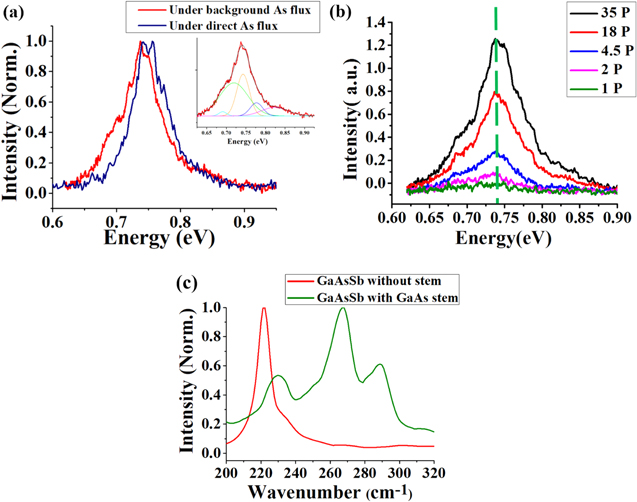
NWs grown under background As pressure exhibit a single dominant photoluminescence peak at 4 K as seen in figure 8(a), while in the other case where an As flux is present only during the growth (and not during Ga droplet formation), PL spectra with higher energy peaks are also observed due to the overall rise in As rich regions within the NWs (figure 8(a)). The PL signal has a peak centered at 0.74 eV with a low FWHM of 38 meV (figure 8(a) inset), which is significantly lower than GaAsSb NWs with a similar Sb composition as reported by Li et al [11]. The low FWHM of the PL attests to the high optical quality of our NWs. Further, good compositional homogeneity of NWs across the sample was proven by replication of 4 K PL on different regions of the NW sample. Shoulder peaks at 0.72 and 0.77 eV have been observed in PL for NWs grown under a background As flux.
Figure 8. (a) 4 K μ-PL spectra for GaAs0.2Sb0.8 NWs grown without stem under a background As flux versus direct As flux; (inset: Gaussian fit of PL for NWs grown under background flux) (b) excitation power dependence of PL peak energy (c) Raman spectra for NWs grown with and without the stem.
Download figure:
Standard image High-resolution image
As can be seen in figure 8(b), invariance of the PL peak position and linear dependence of 4 K PL intensity (not shown) with excitation power indicate the transition to be type-I in nature, which is indicative of a band-to-band transition. Similar invariance with excitation dependence observed in the case of NWs without a droplet at the tip indicates that type-II behavior associated with defect levels previously observed for GaAsSb NWs investigated by Kasanaboina et al [10] is not present in NWs with high Sb content. The 4 K photoluminescence from Sb-rich GaAsSb NW grown under direct As flux shows a peak with PL energy of 0.74 eV, along with higher energy shoulder peaks, suggesting the presence of a region with relatively higher As compositions within the NWs. The use of As direct flux may lead to such additional peaks. The presence of As-rich regions beneath the Ga droplet are the likely cause for such additional peaks from defect levels.
The room-temperature Raman spectrum for GaAs1–xSbx NWs grown using a stem shows dominant GaAs related LO (287 cm−1) and TO (267 cm−1) modes as well as GaSb LO mode at (230 cm−1) as seen in figure 8(c). On the contrary, Raman spectrum of GaAs1–xSbx NWs (Sb/Ga = 6) grown without a stem (figure 8(c)), exhibits only GaSb TO peak at 222 cm−1 and a GaSb LO mode at 232 cm−1. The presence of only GaSb Raman modes and the absence of GaAs and related peaks confirm the lack of a (or a short) GaAs stem that would have given rise to noticeable Raman modes further corroborate the TEM results showing no visible stem. Additionally, this may be viewed as evidence for lack of any Sb-induced defects, attesting to the high microstructural quality of the NWs.
Thus, our systematic and detailed work with substrate temperature and constituent flux variation clearly shows that the growth space is narrow for the synthesis of high quality GaAsSb axial NWs of composition towards Sb-rich corner of the phase diagram. A two-temperature growth approach with low BEP of Ga is found to be critical for the growth on (111) Si without significant parasitic layer. This study thus opens avenues for the NW growth of other multicomponent material systems that may face similar challenges, when grown by the VLS mechanism due to instability in droplets.
4. Conclusion
GaAs1-xSbx (x>0.8) NWs were grown by Ga-catalyzed MBE, with and without stem on Si substrates using high and low Ga BEP, respectively. Coalescence of excess Ga led to a thick 2D layer in the high Ga and Sb BEP regime, while a reasonable yield of vertical NWs without any significant parasitic layer was achieved using low Ga BEP. The use of As background pressure resulted in yield of longer NWs with higher Sb incorporation compared to direct As flux. We have thus successfully demonstrated the growth of high quality ternary GaAsSb NWs of Sb composition exceeding 80 at% on Si (111) substrates, using low Ga BEP and background As pressure. Morphological features such as faceted and shorter NWs, which are unique to III-V antimonide NWs were observed. Low-temperature PL peak energy in the pure GaAs0.2Sb0.8 alloy corresponding to wavelength up to 1680 nm was achieved. The low FWHM of the PL and Raman spectra attest to the excellent quality of the NWs grown. Low Ga BEP and background As BEP work in unison to maximize Sb incorporation in NWs on mismatched lattice substrates, opens the door to new possible investigations of NW growth. This novel technique of growth of high-quality antimonide-based compounds can be extended to the growth of NWs of other similar challenging material system-substrate combination.
Acknowledgments
This material is based upon research supported by the US Office of Naval Research under award number N00014-16-1-2720. This work was performed at the Joint School of Nanoscience and Nanoengineering, a member of the Southeastern Nanotechnology Infrastructure Corridor (SENIC) and National Nanotechnology Coordinated Infrastructure (NNCI), which is supported by the National Science Foundation (ECCS-1542174). The authors acknowledge the use of the Analytical Instrumentation Facility (AIF) at North Carolina State University, which is supported by the State of North Carolina and the National Science Foundation (award number ECCS-1542015). The AIF is a member of the North Carolina Research Triangle Nanotechnology Network (RTNN), a site in the National Nanotechnology Coordinated Infrastructure (NNCI).