

Abstract
In this work, the thermal phase separation and annealing optimization of ZrSiO4 thin films have been carried out. Following annealing optimization, the frequency-dependent electrical characteristics of the Al/ZrSiO4/p-Si/Al MOS capacitors were investigated in detail. The chemical evolution of the films under various annealing temperatures was determined by Fourier transform infrared spectroscopy (FTIR) measurements. The phase separation was determined by x-ray diffraction (XRD) measurements. The electrical parameters were determined via the capacitance–voltage (C–V), conductance–voltage (G/ω) and leakage-current–voltage (Ig–Vg). The results demonstrate that zirconium silicate formations are present at 1000 °C annealing with the SiO2 interfacial layer. The film was in amorphous form after annealing at 250 °C. The tetragonal phases of ZrO2 were obtained after annealing at 500 °C. When the temperature approaches 750 °C, transitions from the tetragonal phase to the monoclinic phase were observed. The obtained XRD peaks after 1000 °C annealing matched the crystalline peaks of ZrSiO4. This means that the crystalline zirconium dioxide in the structure has been converted into a crystalline silicate phase. The interface states increased to 5.71 × 10¹⁰ and the number of border traps decreased to 7.18 × 1010 cm−2 with the increasing temperature. These results indicate that an excellent ZrSiO4/Si interface has been fabricated. The order of the leakage current varied from 10−9 Acm−2 to 10−6 Acm−2. The MOS capacitor fabricated with the films annealed at 1000 °C shows better behavior in terms of its structural, chemical and electrical properties. Hence, detailed frequency-dependent electrical characteristics were performed for the ZrSiO4 thin film annealed at 1000 °C. Very slight capacitance variations were observed under the frequency variations. This shows that the density of frequency-dependent charges is very low at the ZrSiO4/Si interface. The barrier height of the device varies slightly from 0.776 eV to 0.827 eV under frequency dispersion. Briefly, it is concluded that the devices annealed at 1000 °C exhibit promising electrical characteristics.
Export citation and abstract BibTeX RIS
1. Introduction
The great interest in the fabrication and characterization of metal oxide semiconductor (MOS) devices, which consist of different dielectric layers, has mainly arisen due to the wide range of applications of semiconductor-based electronic and optoelectronic devices. The device parameters may exhibit variations depending on the usage area of MOS-based devices, i.e. the gate dielectric thickness is typically less than a few nanometers for devices used in CMOS [1], but a few hundred nanometers is needed for pMOS dosimetric applications [2] in order to enhance device sensitivity. Independently of the device applications, the gate dielectrics and their interface engineering should be investigated in detail. MOS (metal oxide semiconductor) capacitors are common semiconductor devices and are used to determine the structural, chemical and electrical properties of a dielectric material because it is an inexpensive and rapid method. The use of MOS capacitors in technological applications depends on their structural and electrical characteristics, which are directly related to the gate dielectrics and their interfaces with the underlying semiconductors [3–11].
Zirconium silicate (ZrSiO4) is a good possible alternative gate dielectric material, due to its high dielectric constant (k) and thermal stability with silicon [12]. It is well known that silicate groups have very good thermal stability. In particular, zirconium silicate has a sufficient band gap and is compatible for future MOS-based devices. Zirconium silicate is a dielectric material that has been attracting considerable attention thanks to these properties [8, 12–17]. In previous studies, Wilk G D et al [18] reported that zirconium silicate exhibits excellent electrical properties and high thermal stability in direct contact with Si. In addition, the Gibbs free energies governing the Zr-Si-O system lead to a ternary phase diagram; however, it was not revealed how their phase diagrams change with the annealing temperature. Albena Paskaleva [19] indicated that further optimization of the properties of ZrSiO4 films should be undertaken to reduce trapping by taking the appropriate annealing and interface engineering steps. In the studies of Morais J et al [20], in which ZrSixOy thin films are subjected to thermal annealing, experimental studies have shown that the interface between ZrSixOy films and the Si bottom layer remains stable. However, while a detailed chemical analysis has been carried out in this study, no study has been done on how the electrical properties change due to annealing. It has been reported that one of the important parameters is the different variety of annealing treatments. The different annealing temperature not only affects the structural properties of high-k films but also the electrical properties. For this reason, it is important to know how the different annealing temperatures affect the electrical properties of zirconium silicate MOS capacitors. Many defective structures may occur depending on the production methods. Border traps, mobile ionic charges and oxide trapped charges are examples of these defects. Suitable annealing temperatures are really important if these undesirable conditions are to be eliminated. The thin films of zirconium silicate were annealed at 250 °C, 500 °C, 750 °C and 1000 °C in a nitrogen environment. The thin film bond structures were analyzed by Fourier transform spectroscopy. Changes in the phase diagrams can clearly be observed using this spectroscopy method. Some frequency-dependent states, which include the surface state and the interface state, affect the ideal behavior of the produced MOS capacitors, depending on the AC voltage signal. In particular, at high and low frequencies, it is necessary to study the behavior of the MOS capacitors [5, 12, 21, 22].
In this work, the first aim is to determine the optimum annealing conditions and initial device characteristics of ZrSiO4-based devices for use in microelectronic pMOS dosimetry applications in further studies. Secondly, bond creation through Zr-O-Si was investigated to learn how to change the dependency on the annealing temperature. Finally, frequency-dependent electrical characterizations of the most suitable zirconium silicate MOS capacitors were investigated in detail. Some important parameters, namely the interface state and barrier potential [12, 22–24], were calculated by eliminating the series resistance effect.
2. Experimental details
The 500 μm Si p-type 〈100〉 substrates with a resistivity of 1–4 Ω, were cleaned by the standard Radio Corporation of America (RCA) cleaning process in order to fabricate the ZrSiO4 thin films. Following the RCA process, the cleaned wafers were loaded immediately into the sputtering chamber for ZrSiO4 deposition onto the silicon surface. A ZrSiO4 target with a diameter of 4 inches and a purity of 99.99% was used for the deposition of the oxide layers. The sputtering base chamber pressure was left to settle to less than 6.0 × 10⁻⁴ Pa and the Ar gas flow was adjusted to 16 sccm. The sputtering pressure was adjusted to be 1.0 Pa, and then pre-sputtering was performed at 300 watts for about 150 min to remove any impurities on the ZrSiO4 target surface. After pre-sputtering, sputtering was performed without wasting any time under the same parameters for 45 min. The thickness of the films was measured to be about 120 nm by a spectroscopic reflectometer. The ZrSiO4/p-Si films were divided into four pieces and one of the pieces was not annealed. However, the others were separately annealed at 500 °C, 750 °C and 1000 °C for 40 min in a nitrogen environment. The effect of annealing on the general chemical structure was investigated by ATR- FTIR measurements. After that, high-purity aluminum (Al) metal (99.999%) was deposited using the sputtering system on the front and back surface of all the thin films. In addition, a 1 mm diameter circular shadow mask was used during the deposition of the front contacts in order to determine the electrical characterizations. The annealing influence on the electrical characteristics of the fabricated Al/ZrSiO4/p-Si/Al MOS capacitors was determined using capacitance–voltage (C–V) and conductance–voltage (G/ω−V) measurements at 1 MHz. Following annealing optimization, detailed electrical characterizations under frequency dispersion (50 kHz, 100 kHz, 250 kHz, 500 kHz and 750 kHz and 1 MHz) were carried out to check that the device exhibited optimum characteristics after annealing. Before analyzing the electrical characteristics of the devices, a series resistance correction was performed for the given C−V and G/ω−V measurements in this work in order to eliminate possible signal losses and analyze the real device characteristics [25, 26].
3. Results and discussion
3.1. FTIR and XRD results
The structural properties of the thin films annealed at different temperatures were investigated by using ATR-FTIR. ATR-FTIR measurements were performed to examine the types of chemical bond in the obtained films. The peaks at 2150, 2025 and 1980 cm−1 were labeled as an asymmetric SiH2 vibration. The SiH3 and SiH absorption peaks may have been caused by the HF treatment of the silicon wafer, respectively [27]. The broad peaks near 1065 and 1200 cm−1 were assigned to the Si-O-Si absorption of the silicon wafer. The density of the Si-O-Si bonds became more evident after annealing at 750 °C. In addition, as the annealing temperature of the films increased, the intensity of the Si-O stretching bands of the Zr-Si-O also increased and were detected near 800 and 840 cm−1 [28]. These peaks cannot be seen as clearly as those present at the lower annealing temperature. Moreover, a Zr-O-Zr vibration was observed at 520–600 cm−1 [29] during the high-temperature annealing. It can be observed that in figure 1, the concentration of the Zr-O-Zr bonds increased at an annealing temperature of 750 °C. However, in the samples annealed at 1000 degrees, when the Zr-O-Zr peak intensities decrease, the Zr-O-Si peak intensities increase. This observation implies that the high temperature transforms ZrO2 bonds into ZrSiO4.
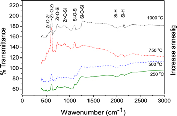
Figure 1. A Fourier transform infrared spectroscopy (FTIR) measurement of ZrSiO4 thin films at different annealing temperatures.
Download figure:
Standard image High-resolution imageThe phase identification study of the ZrSiO4 thin films was undertaken using XRD measurements. The XRD diffraction patterns of the annealed samples at different temperatures are shown in figure 2. No crystallographic orientations can be observed after annealing at 250 °C, which means that the ZrSiO4 layer which annealed at a low temperature is in an amorphous form. The tetragonal ZrO2 phase appears to be dominant in the annealed samples at 500 °C. The peak appearing around 48.20 degrees corresponds to a mixture of both tetragonal and monoclinic ZrO2 phases. When the annealing temperature rises to 750 °C, the ZrO2 tetragonal peak intensity is markedly reduced, while the monoclinic phase becomes stronger. It is obvious that the phase starts to change from a tetragonal to a monoclinic phase when the temperature approaches 750 °C, which is in agreement with [30]. A further increase in the annealing temperature also causes significant changes in the crystallographic structure. The peaks obtained after 1000 °C annealing matched the crystalline peaks of ZrSiO4 (ICCD card no: 06-0266). This means that the crystalline zirconium dioxide in the structure has been converted to a crystalline silicate phase. A similar phase transition has also been observed for Hf-based silicate thin films [31], so the same physical/chemical mechanism may be valid for the Zr silicate layer in this study. FTIR analyses also support the observations obtained from XRD diffraction.

Figure 2. The XRD diffraction patterns of ZrSiO4 thin films at different annealing temperatures.
Download figure:
Standard image High-resolution image3.2. Annealing influence on electrical properties
3.2.1. Annealing influence on capacitance–voltage and conductance–voltage characteristics of devices
The capacitance–voltage measurements of the Al/ZrSiO4/p-Si/Al MOS capacitors were obtained at a high frequency (1 MHz). The effects of annealing temperatures on the capacitance and conductance charateristics are shown in figure 3 and figure 4, respectively. It can be observed that the measured capacitance of the devices significantly changes with the annealing temperature. The capacitance values of the as-deposited and annealed samples at 500 °C are lower than those for the samples annealed at a high temperature. The large numbers of dangling bonds in the device structure after sputtering deposition and the annealing temperature of 500 °C probably do not provide enough free energy to form a complete bond. The lower intensities of the transmission peaks in the FTIR measurements support this discussion. The dangling bonds behave like a trapping center [32] and these centers may be dispersed within the dielectric layer. Due to the presence of these trap centers and dangling bonds, the dielectric properties of the ZrSiO4 can be degraded. In addition, the crystallographic phases of the film layer have been changed with the annealing temperature, as mentioned above. It is known that changes in the crystallographic structure may affect the dielectric properties of the layer [33, 34], possibly due to variations in the molar volume. Hence, a rise in the capacitance values is associated with the improvement of the dielectric constant of the ZrSiO4 layer, either passivation of the dangling bonds or phase changes under high-temperature annealing. Moreover, a rise in the capacitance at the inversion layer can be observed, especially after annealing at 1000 °C. The variation in the inversion capacitance is associated with the complete formation of an interfacial SiO2 layer during the oxidation of ZrSiO4. The fluctuations on the conductance curves in figure 4 are also associated with evolution of interface chemistry under thermal annealing. This evolution become more visible in further interface state density calculations. On the other hand, the flat band voltage in table 1 exhibits the variation due to trapped charges and the formation/breaking of new bonds depending on the thermal energy. Moreover, the border trap density (Nbt) has been calculated to assess the oxide quality numerically using equation (1) from the flat band shift (ΔVfb,hys) in the capacitance hysteresis (not shown here),

where Cox (= εoxεoA/d) is the oxide capacitance, q is the electrical charge and A is the front contact area. The measured ΔVfb,hys and the calculated Nbt are tabulated in table 1. As seen from table 1, the Nbt values decrease with the annealing temperature. This behavior also demonstrates the passivation of the dangling bonds and the rise in oxide quality. Moreover, the conductance measurements were also measured to specify the behavior of the interface states depending on the annealing temperatures.

Figure 3. C–V curves carried out for high frequency (1 MHz) in MOS capacitors with different annealed ZrSiO4 films.
Download figure:
Standard image High-resolution image
Figure 4. G/ω–V curves carried out at a high frequency (1 MHz) for MOS capacitors with different annealed ZrSiO4 films.
Download figure:
Standard image High-resolution imageTable 1. Annealing effects on the electrical parameters of Al/ZrSiO4/p-Si/Al MOS capacitors.
| Vfb (V) | Dit × 1010 (cm−2) | ΔVfb,hys (V) | Nbt × 1010 (cm−2) | |
|---|---|---|---|---|
| 1000 | −0.23 | 6.71 | 0.11 | 7.18 |
| 750 | 1.51 | 3.33 | 0.14 | 9.14 |
| 500 | 1.99 | 4.81 | 0.22 | 14.4 |
| 250 | −0.32 | 2.13 | 0.35 | 22.9 |
Variations in the peak intensities can be observed with the annealing temperature. The interface state densities (Dit) have been calculated numerically by using equation (2)

where Gmax/ω is the peak value of the Gmax/ω–V curve, and C is the capacitance of the MOS corresponding to Gmax/ω. The calculated Dit values at various annealing temperatures are given in table 1. It is interesting that the lowest Dit value is found in the annealed samples at 250 °C. It is known that high-temperature annealing may have a complex influence on the interface chemistry. In other words, some new bonds may be formed at the interface between the dielectric/Si when some bonds are broken. This reaction may have been possible, considering the FTIR measurement, because the oxidation and formation of the Zr-O-Si bonds was almost completed after 750 °C annealing, resulting in a decrease in the Dit. When the temperature approaches 1000 °C, the Si starts to bond with the Zr and the formation of Zr-Si-O bonds occurs. Hence, during the reaction at 1000 °C, it is possible for the Zr-O bonds to break and new Zr-Si-O bonds to occur [35–37]. A slight rise can be observed in the Dit value upon annealing at 1000 °C. This behavior may be associated with an incomplete reaction and some of the dangling bonds generated by broken Zr-O-Si at the interface; also the formation of SiOx in the interfacial layer may have contributed to this behavior. On the other hand, the lattice expansion/mismatch due to local crystallization of the ZrSixOy/Si interface [38] may also have contributed to the rise in the Dit value. The calculated Dit values, which are almost of the same order as the high-quality SiO2/Si interface, are 1010 cm−2. The first principle calculation study performed by Puthenkovilakam et al [39] reported that an excellent interface with silicon can be obtained for a ZrSiO4/Si stack. Hence, the obtained results in this study prove the first principle calculations experimentally. Considering the FTIR and electrical analysis, 1000 °C is the optimum annealing temperature for good silicate formation, the lowest oxide trap density and promising interface quality.
3.2.2. Annealing influence on gate leakage current characteristics of devices
The leakage current as a function of various annealing temperatures with voltage sweeps both in the accumulation and inversion regions is given in figure 5. It can be observed that at −1 V, the leakage currents for the devices annealed at 250 °C, 500 °C, 750 °C and 1000 °C are 3.5 × 10⁻⁹ Acm−2, 2.07 × 10⁻⁶ Acm−2, 1.25 × 10⁻⁶ Acm−2 and 4.17 × 10⁻⁷ Acm−2, respectively. The order of the leakage current was varied from 10−9 Acm−2 to 10−6 Acm−2, which is promising for dielectric applications. But considering the gate oxide thickness, the leakage current values are quite normal. On the other hand, a significant increase in the leakage current can be observed after 500 °C annealing of the ZrSiO4 devices compared to the 250 °C annealing characteristics. The increment in the crystallization degree could be the main reason for the enhancement of the leakage current after 500 °C annealing. It has been reported that grain boundaries may act as leakage paths where mobile charges can be transported through the percolation path along the grain boundaries in crystalline films [40–42]. The decrement in the leakage current with higher annealing temperatures may be attributed to the improvement in the oxide quality [43, 44], i.e. a reduction in the oxide/border charges seen in table 1, passivation of the dangling bonds and complete formation of the silicate structure.

Figure 5. The leakage current density versus the voltage characteristics for ZrSiO4 MOS capacitors at different annealing temperatures.
Download figure:
Standard image High-resolution image3.3. Frequency-dependent electrical properties
The frequency dependencies of the electrical characterization of the devices annealed at 1000 °C have been studied, following the annealing optimizations. The device behavior under the applied voltage frequency C–V and G/ω characteristics are given in figures 6(a) and (b). A very slight increase in the capacitance values can be observed with decreasing applied voltage frequencies. This low sensitivity shows the lower frequency-dependent interface state densities and excellent interface quality. In other words, the time-dependent interface states may act as an additional capacitance (Cit) and contribute to the measured capacitance characteristics. The equivalent capacitance circuit can be seen in figures 7(a) and (b) with the interface state capacitance (Cit) contribution incorporated [4]. Figures 7(a) and (b) demonstrate that if the lifetime (τ) of the interface states (τ = CitRit, where Rit is the resistance associated with the interface states) is lower than the applied voltage frequency (1/ω), the states can easily respond and contribute measured capacitance values at lower frequencies. However, the interface states do not have enough time to follow the applied frequencies at higher frequencies, hence, the contribution to the measured capacitance is almost zero [7, 45, 46]. The higher Cit value causes high variations in the capacitance values under frequency dispersion. However, only a very slight rise in capacitance can be observed in any of the interface qualities, and these insensitivities can improve the reliability of microelectronic applications.
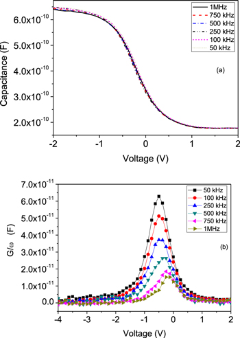
Figure 6. The frequency dependent (a) C–V and (b) G/ω–V curves of Al/ZrSiO4/p-Si/Al ZrSiO4 MOS capacitors.
Download figure:
Standard image High-resolution image
Figure 7. The equivalent circuit diagram at (a) low- and (b) high-frequency regions of the MOS capacitors.
Download figure:
Standard image High-resolution imageWhen a small AC signal is applied to the MOS capacitors, a carrier interchange between the interface state and the carrier majority bond semiconductor occurs. In particular, the Fermi energy may move slightly downward or upward depending on the interface state impact, i.e. if the states are occupied or empty [7]. The interface trap close to the band limits can quickly capture and release carriers depending on the applied voltage frequency and interface state response time. Hence, the observed rise in the conductance in figure 6(b) is associated with reordering and construction between the interface states and the majority carrier band of the semiconductor under various applied voltage frequencies. The variations in the conductance characteristics verify the presence of the different time-dependent responses of the interface states [47]. Using the conductance peaks in figure 6(b), we have calculated the interface state density using equation (2) and the frequency- dependent Dit characteristics are also illustrated in figure 8. The expected rise in the Dit values under low frequencies can be observed. The amount of various interface states between the lowest (50 kHz) and the highest (1 MHz) does not dramatically change, and a slight variation/low interface state density is still observed compared to the other promising dielectrics reported in [7, 48, 49].
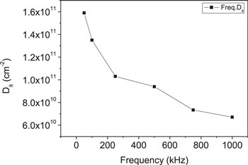
Figure 8. The variations of Dit as a function voltage for the ZrSiO4 Al/ZrSiO4/p-Si/Al MOS capacitor.
Download figure:
Standard image High-resolution imageThe linear region close to the depletion, corresponding to the inversion reciprocal squared of the capacitance (C−2) characteristics, have been used to calculate the barrier potential (ϕB) of the ZrSiO4 under frequency dispersion. The C−2 curves and the fitted function C−2 curves are plotted in figure 9 for each measurement capacitance and voltage curve at different frequencies. A good linear relation with a 99.1% match between data points and the fitted function curves indicates that the interface states have a low concentration and are uniformly distributed [7]. The correlation between C−2 and V is obtained using the following equation:

where the front area of the MOS capacitor is A, εs is the dielectric constant of the semiconductor, q is the electric charge, V is the applied voltage, V0 (= Vd − kT/q) is the intersected line with the voltage axis, and Nd is the doping concentration of the p-type Si wafer found from the slope of the C−2–V curve and [12, 17, 22]. The value of ϕB can be calculated by using equation (4):
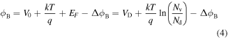
where VD is the diffusion potential, Nv is the effective density of states in the valence band and ΔϕB is the image force barrier lowering given by

where  is the maximum electric field. The calculated ϕB and some important calculation parameters are tabulated in table 2. Slight variations in EF can be observed due to the diffusion of charge carriers from the interface changes with the frequency [50]. It is also observed that the ϕB values were enhanced from 0.776 eV to 0.827 eV upon increasing the frequency. Peacock et al [51] calculated the electron barrier conduction band offset values to be 1.5 eV for ZrSiO4 using the CASTEP code. However, the calculated ϕB was lower than the theoretic value of 1.5 eV. The presence of a defect level in the gate oxide and Si may act as a recombination center and may also act as a channel for electron transport, resulting in the decline of the barrier potential [52]. Although the value of ϕB is lower than the theoretic value, it still acts as an acceptable potential barrier for electron tunneling/conduction [53]. The change of ϕB can be attributed to the time-dependent defect level in the band gap of the ZrSiO4, especially in the ZrSiO4/Si interface [54, 55].

Figure 9. The C−2−V curves of the Al/ZrSiO4/p-Si/Al MOS capacitor under frequency variations.
Download figure:
Standard image High-resolution image
Table 2. The frequency-dependent electrical parameters of the Al/ZrSiO4/p-Si/Al MOS capacitors.
| Frequency | VD (eV) | Nd × 1015 cm−3 | EF (eV) | Δ ϕB (meV) | ϕB (eV) |
|---|---|---|---|---|---|
| 1000 | −0.6460 | 9.47 | 0.2049 | 0.0230 | 0.827 |
| 750 | −0.6290 | 9.37 | 0.2052 | 0.0228 | 0.811 |
| 500 | −0.6260 | 9.53 | 0.2048 | 0.0227 | 0.808 |
| 250 | −0.6080 | 9.40 | 0.2051 | 0.0226 | 0.790 |
| 100 | −0.601 | 9.58 | 0.2046 | 0.0226 | 0.782 |
| 50 | −0.5940 | 9.64 | 0.2045 | 0.0226 | 0.776 |
4. Conclusion
The optimum thermal annealing conditions for ZrSiO4 thin films have been established in ambient nitrogen conditions. It was observed that O-Zr-O and O-Si-O bonds create new bonds forming Zr-Si-O at high annealing temperatures. The measured capacitance–voltage values and FTIR results support this situation. The interface state density increases with the annealing temperature; the number of border traps decreases. This situation is actually quite compatible with the literature. So, it is obvious that the 1000 °C annealing temperature is very suitable for this dielectric material. Afterwards, the detailed electrical characteristics of the Al/ZrSiO4/p-silicon MOS capacitors were determined at various voltage frequencies. Considering the results of the study, the small variations in the frequency dispersion for the C–V measurement demonstrate the lower frequency-dependent interface state densities and excellent interface quality of the material. The conductance is sensitive to the applied voltage frequencies. This sensitivity is due to the charges that are dependent on the frequency such as the interface state charges and border trap charges. The interface states are highly compatible with the literature, i.e. the effects of interface states appear at low frequencies. However, the frequency-dependent interface states do not show significant variation. This behavior is closely related to the interface quality. Although the calculated barrier potential is slightly lower than that in the literature, it still does not cause a problem in terms of MOS-based technology. Briefly, in light of the obtained results, the initial device characteristics of the Al/ZrSiO4/p-Si/Al MOS capacitor with a 120 nm gate dielectric thickness exhibit promising electrical characteristics for micro-electric applications, especially for MOS devices to be used in radiation dosimetry. Further study will concern the radiation responses of the optimized devices and the possibility of using ZrSiO4 as a sensitive layer in pMOS dosimetry.
Acknowledgments
This work was supported in part by the Ministry of Development, Turkey, under contract 2016K121110, in part by Abant Izzet Baysal University, Bolu, Turkey, under contract BAP. 2015.03.02.870.