

Abstract
Lowering the temperature of crystallization by deposition of thin films on a heated substrate represents the easiest way to find new means to develop and improve new working devices based on nanocrystals embedded in thin films. The improvements are strongly related with the increasing of operation speed, substantially decreasing the energy consumption and reducing unit fabrication costs of the respective semiconductor devices. This approach avoids major problems, such as those related to diffusion or difficulties in controlling nanocrystallites size, which appear during thermal treatments at high temperatures after deposition. This article reports on a significant progress given by structuring Ge nanocrystals (Ge-NCs) embedded in silicon dioxide (SiO2) thin films by heating the substrate at 400 °C during co-deposition of Ge and SiO2 by magnetron sputtering. As a proof-of-concept, a Si/Ge-NCs:SiO2 photo-sensitive structure was fabricated thereof and characterized. The structure shows superior performance on broad operation bandwidth from visible to near-infrared, as strong rectification properties in dark, significant current rise in the inversion mode when illuminated, high responsivity, high photo-detectivity of 1014 Jones, quick response and significant conversion efficiency with peak value reaching 850% at −1 V and about 1000 nm. This simple preparation approach brings an important contribution to the effort of structuring Ge nanocrystallites in SiO2 thin films at a lower temperature for the purpose of using these materials for devices in optoelectronics, solar cells and electronics on flexible substrates.
Export citation and abstract BibTeX RIS
1. Introduction
In the past decades, nanostructured materials have been the focus of many research groups due to their improved structural, optical and electrical properties, appropriate for various practical applications. Quantum confinement effect (QCE) is more powerful in bulk Ge compared to Si because of Ge greater excitonic Bohr radius (approximately 24 nm in the case of Ge and about 5 nm for Si) [1, 2]. Also, compared to Si, Ge has higher lattice parameter, carrier mobility and smaller energy gap, thermal conductivity or effective mass of the carriers [3]. Ge lower melting temperature of 938.3 °C (compared to 1414 °C for Si) and its compatibility with well-developed Si technology represent other major advantages that allow obtaining Ge-NCs at a lower temperature. All the above-mentioned advantages suggest that it would be much simpler to shift the electronic structure near the band gap of Ge [4, 5]. Controlling the morphology and Ge high diffusivity (that appear at high annealing temperatures) of nanocrystallites would facilitate advances in understanding their quantum confinement behavior and an easier evaluation of their performances for the potential inclusion in new devices [6, 7]. Nanostructured Ge embedded in SiO2 thin layer has a significant absorption coefficient because of localized states at the Ge/SiO2 interface and higher optoelectronic conversion efficiency [8]. Devices using such functionalized thin layers are photo-sensitive and they show high responsivity within a broad wavelength range from ultraviolet, through visible to near-infrared (NIR) making them materials of choice for many technological applications in sensing, spectroscopy, imaging, communication [9, 10], optoelectronic devices [11], light emitters [12] and solar cells [13]. These properties are attributed to the Ge-NCs QCE, much stronger than in the case of Si or to interface carrier traps between Ge-NCs and the surrounding SiO2 matrix [14–17]. As a comparison, it has been demonstrated that photo-sensitive structures based on silicon nanocrystallites (Si-nps) can achieve peak responsivity in the range of 0.4–2.8 AW−1, and optoelectronic conversion efficiency as high as 200% [18] whereas Ge-NCs-based photo-sensitive devices are even more promising, as the maximum responsivity reported so far is 1.8 AW−1 at −2 V and about 4 AW−1 at −10 V, respectively. The resulting optoelectronic conversion efficiency was 300% obtained at −2 V bias and 700% at −10 V, respectively [8]. The properties of Ge-NCs incorporated into SiO2 matrix can be strongly influenced by difficulties related to the control of the technological parameters of the deposition and/or to the inevitable formation of defects regardless of the preparation method (sputtering [19], implantation [20] or epitaxial [21]). Structuring of Ge-NCs embedded into SiO2 has been achieved so far by thermal annealing after deposition of Ge/SiO2 thin layers, or by thermal oxidation of SiGe layers, at high temperature, in excess of 700 °C [22, 23]. This range of temperature is lower than the temperature needed to obtain Si-nps (typically around 1100 °C), but it is still too high to be appropriate for processing structures and devices on flexible or glass substrates. This is the present challenge to be solved in order to benefit from the advantages in terms of reducing manufacturing cost and much broader range of applications [24, 25].
It is crucial to significantly lower the temperature for structuring Ge-NCs into SiO2 matrix in order to use these materials in Si-based optoelectronics on a chip, where low processing temperature is needed to preserve the functionality of the adjacent Si electronics [26]. There have been attempts to structure Ge-NCs at temperatures below 400 °C, but the technological methods employed (ultra-high vacuum chemical vapor deposition or wet chemical synthesis) are either too expensive and/or incompatible with the current highly developed silicon technology [27, 28]. The reported attempts using thin films grown by magnetron sputtering for structuring embedded Ge-NCs by post-deposition thermal annealing at 400 °C show that the obtained Ge-NCs are amorphous and the photo-response properties are weak [8].
In this work an innovative procedure is reported. It was developed to perform the synthesis of Ge-NCs in SiO2 layer during deposition, by heating the substrate at 400 °C (a temperature higher than the one specific to the deposition process). This is much lower than the temperature needed for structuring the Ge-NCs by post-deposition thermal annealing. We proved the feasibility of the fabrication procedure through an Al/Si-n/Ge-NCs:SiO2/ITO photo-sensitive structure obtained by magnetron sputtering method while heating the substrate. These structures tested at room temperature exhibit superior performances like great responsivity, quick response and high optoelectrical conversion efficiency upon broadband, from about 450 nm to approximate 1300 nm, with peak value reaching 850% at −1 V applied bias and about 1000 nm. Optoelectronic devices fabricated by our approach can lead to optimized design strategies for infrared absorbers that can be used in Si-based multi-junction solar cells, for faster and highly photo-sensitive devices based on Ge-NCs or to integrated optoelectronics on Si or flexible substrates.
2. Experimental
2.1. Materials and methods
SiGeO2 thin films containing Ge-NCs were fabricated on clean 10 mm × 10 mm, n-type (100) Si substrates, with bulk resistivity in the range 10–20 Ωcm, by magnetron sputtering depositing, at the same time, SiO2 and Ge from separate three inches sputtering targets (Gamma1000 tool from Surrey Nanosystems). The Si pieces used as substrates were degassed for 5 min in vacuum at 200 °C. Deposition chamber was evacuated down to 1 × 10⁻⁷ Torr before deposition. To achieve targeted 50:50 concentration ratio of Ge into SiO2 during deposition, technological parameters like direct current (DC) or radio frequency (RF) power, argon gas pressure, and substrate temperature were finely tuned to optimized values of 30W DC, 262W RF, 4 mTorr and 400 °C, respectively. Substrate rotation contributed to the superior quality of the layer (about 250 nm) and a good Ge distribution into SiO2.
Electrical and photoelectrical measurements at room temperature were performed on Al/Si-n/Ge-NCs:SiO2/ITO structures after the Al back electrode and indium–tin-oxide (ITO) matrix top electrodes (3 × 3 mm2) were deposited by e-beam evaporation (Bestec) and magnetron sputtering (Varian ER3119), respectively, using shadow masking.
2.2. Characterization
The structure investigations on GeSiO2 layers were performed by x-ray diffraction (XRD) (AXS-BRUKER,  with λ = 0.15406 nm), SPECS x-ray Photoelectron Spectroscopy (XPS) with an analyzer (PHOIBOS 150) and transmission electron microscopy (TEM) using analytical atomic microscope (JEOL, JEM ARM 200F).
Electrical studies were performed on a setup which contains a cryostat provided with optical windows (CCS450 from Janis), a Keithley electrometer (6517A) and a 331 LakeShore controller for temperature. The evaluation of the photo-response properties of the investigated layers was done using three light sources in the measurements: a Xe lamp (450 W) combined with a 1/4 Newport monochromator to provide a monochromatic beam between 200 and 2500 nm, a tungsten-halogen lamp (20 W, Newport) and a laser diode as a more powerful laser source in the NIR domain at 808.5 nm. The reflectance spectra have been taken at a fixed angle of incidence (6°) using a double beam spectrophotometer (0.25–3 μm, 950 Perkin Elmer) with specular reflectance fixture (B 0086703). The operation speed investigations of the photo-sensitive structure were evaluated using a mechanical modulator (SR 540) and an oscilloscope (500 MHz WaveJet) together with a standard commercial detector (PDA10CS EC).
3. Results and discussions
In this section, the results of structural investigations, electrical characterization, photoelectrical and response time properties of the SiO2 thin films formed with embedded Ge-NCs and the obtained optical sensitivity of the structure are presented and discussed. To reveal the crucial contribution of Ge-NCs, two types of structures were realized:  single thin layer of Al/Si-n/Ge-NCs:SiO2/ITO test structure and
  a similar reference structure Al/Si-n/SiO2/ITO, with no Ge added.
Diffraction spectrum measured on one of the Ge-NCs:SiO2 layer deposited on Si substrate heated at 400 °C during deposition is presented in figure 1(a), which includes the standard XRD tabulated pattern (Inorganic Crystal Structure Database—ICSD:79-0001) of Ge cubic. The plotted diffractogram shows maxima corresponding to (111), (220) and (311) Ge cubic structure. It can be observed that diffraction peaks are broad, indicating the presence of small nanocrystals, of about 4.5 nm as estimated using Scherrer equation. Figure 1(b) present the XPS spectra of the Ge 3d core levels. The spectra suggest that the investigated films contain GeO2 and GeOx subspecies of Ge.

Figure 1. GeSiO2 thin film containing Ge-NCs structured in-situ during deposition of Ge and SiO2 on a Si substrate heated at 400 °C: (a) x-ray diffractogram and (b) XPS spectra of the Ge3d level pointing the oxidation states of Ge existent in the GeSiO2 layer.
Download figure:
Standard image High-resolution imageThe high resolution (HR)TEM picture of the cross section (XTEM) specimen (figure 2 (a)) shows in detail the interface between Si substrate, native SiO2 film and the deposited Ge-NCs:SiO2 layer. Segregation of Ge nanoparticles forms a band at the interface between native SiO2 and Ge-NCs:SiO2 film, as a result of deposition conditions. EDX spectrum (inset figure 2 (a)) recorded on Ge-NCs:SiO2 film demonstrates that Si and Ge were deposited in equal atomic concentration. The HRTEM image of Ge-NCs:SiO2 film presents the distribution of Ge-NCs (∼5 nm) in the amorphous SiO2 (figure 2(b)). The inset shows an oriented Ge-NC. The microscopy results confirm the crystallinity of the Ge grains, previously suggested by XRD.
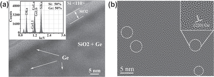
Figure 2. HRTEM pictures: (a) Ge-NCs:SiO2/native SiO2/Si interface with EDX spectra (inset); (b) spatial distribution of Ge-NCs within the SiO2 layer with an oriented Ge-NC (inset).
Download figure:
Standard image High-resolution imageFigure 3(a) shows a drawing of the investigated structure. Figure 3(b) shows the schematic representation of the electrical transport mechanism in the Al/Si-n/Ge-NCs:SiO2/ITO system. The electrons are tunneling from the upper contact (ITO) to the Ge-NCs incorporated into the SiO2 film and they move inside the active Ge-NCs:SiO2 layer percolating between neighboring Ge-NCs [29]. The active area of the photo-sensitive structure is 9 mm2. The results of 'on/off' measurements, which reveal the photovoltaic behavior of the structure, are represented in figure 3(c). The two characteristics are recorded at two different values of the incident optical power (Popt—the optical power incident on the active zone of the structure), respectively 5mW and 20 mW. These measurements were performed under a continuous illumination using an incandescent lamp (20 W, tungsten-halogen). The Popt was measured using a neutral power meter (LaserStar). The resulting open-circuit voltage has values between 120 and 150 mV depending on the applied optical power, which emphasizes the great optical sensitivity of the investigated structures, proving their suitability for optoelectronic applications. It is known that a structure with photo-voltaic properties can work without external bias applied. Such a self-powering photo-sensitive device is a promising nominee for developing new devices with high sensitivity at reduced scale, hence low cost.
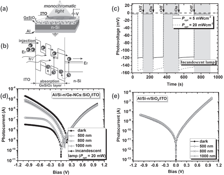
Figure 3. Electrical characterization: (a) schematic representation of the photo-sensitive test structure and measurement geometry; (b) transport mechanism—schematic representation of the photoresponse; (c) photovoltage measurements performed at Popt of 5 mW and 20 mW respectively, on a capacitor-like photo-sensitive structure (Al/Si-n/Ge-NCs:SiO2/ITO); (d) I–V curves of a photo-sensitive structure with Ge-NCs; (e) I–V curves of the similar structure without Ge incorporated into the SiO2 layer. The characteristics plotted in figure 3 (d) and (e) were obtained for photo-sensitive structure in the dark, under illumination with incandescent lamp (Popt = 20 mW) and monochromatic illumination (500, 800 and 1000 nm), respectively.
Download figure:
Standard image High-resolution imageIn figure 3(d) current–voltage (I–V) characteristics obtained in dark, under illumination using a tungsten-halogen lamp (Popt = 20 mW) and respectively continuous illumination at different monochromatic wavelengths is plotted. The dark current level is slightly higher than expected for Ge-NCs incorporated in a stoichiometric SiO2 matrix and this can be related to SiO2 deviation from stoichiometry and chemical reduction of GeOx (presented in figure 1(b)), which is the major mechanism for controlling the size of Ge-NCs. It is known that, even slight deviations from stoichiometry can create defects into the matrix, which are favorable for photovoltaic applications in the case of GeSiOx films with a low oxygen deficiency (x < 2) [30, 31].
For the investigated structures, the voltage onto ITO contact has been applied in the range −1–1 V (in steps of 20 mV) and the silicon substrate was earthed. For such structures, the bias voltage splits across a few junctions, as the interface formed between ITO top electrode and Ge-NCs:SiO2 layer, active layer (Ge-NCs:SiO2) zone or those located at the Ge-NCs:SiO2/native oxide/Si interface [20]. According to the studies leaded by Castrucci et al the native SiO2 separation zone observed from microstructure investigations is formed at the Si/Ge-NCs:SiO2 interface and it acts like a junction generating a relative inflexion of Si and Ge conduction and valence bands (Ge-NCs continuous layer) that makes a depletion layer into the Si substrate [32]. Characteristics performed in the dark, at ±1 V bias voltage, exhibit low currents and a rectifying behavior of about 102 ratio between positive and negative sides. The unidirectional behavior (rectifying) may be the result of the complex junctions present in the investigated structures which operate as a rectifying diode-like contacts. The characteristics are almost unchanged under illumination (continuous illumination with an incandescent lamp) at forward bias, but a significant rise of current of about 103 times is observed under reverse bias thanks to electron-hole couple photo-generated in the Ge-NCs and Si-n substrate. In this case, both electrons and holes move percolating through the Ge-NCs network. Thus, a dynamically trapped positive charge is produced improving the electron injection and hence growing the rate of process and directing to a sharp increase of photoresponse also due to barrier lowering under illumination. The active layer (Ge-NCs:SiO2) acts as a network of resistors in which every Ge-NC is tied with its Ge-NCs neighbors through a finite tunneling resistor. So, the charge careers from Ge-NCs would pass by tunneling towards their neighboring Ge-NCs choosing the path with the smallest resistance. An analogous mechanism was proposed by Hsu et al [33]. The photo-response properties of the structure are directly associated with generating mechanism and to collecting of electron and hole as pairs. To emphasize the role played by the Ge-NCs within the structure, we also fabricated a reference structure (Al/Si/SiO2/ITO) where the total SiO2 film thickness is the same as the GeSiO2 layer from test structure, but no Ge was embedded.
Characteristics obtained on the reference structure are presented in figure 3(e). The dark current is much smaller (−4.2 × 10⁻⁹ A at −1 V) under reverse-bias compared to the photo-sensitive test structure that contain Ge-NCs (−3.3 × 10⁻⁸ A at −1 V), because the carrier tunneling rate through the SiO2 dielectric is much lower. The absence of Ge-NCs leaves the structure insensitive to light, proving the key role played by the Ge-NCs on radiation sensing properties of the structure.
The experimental setup for studying the wavelength dependence of responsivity (Rs) is represented in figure 4(a). The calculated Rs, plotted in figure 4(b), as the ratio of the photocurrent generated in the structure and the optical power incident on the investigated zone for different values of reverse bias (−0.1 V, −0.5 V and −1 V respectively), were obtained using the following equation [34]:

where Iphoto is the current obtained from the structure under illumination. Popt was determined using a powermeter (Ophir by LaserStar) equipped with a 3A-P-SH-V1 sensor. The photo-sensitivity of the structure under −1 V bias exceeds 5 AW−1 at a wavelength of about 1000 nm. Increasing the density of Ge-NCs into SiO2 or by optimizing the Ge-NCs size represent the main possible ways that can lead to widen the high responsivity spectral range. The responsivity characteristics do not account for the light reflected from the structure, and consequently one cannot make a clear correlation between the photogeneration of carriers and contribution of physics phenomena involved. The reflectance spectra for Ge-NCs:SiO2 thin film deposited in-situ at 400 °C on Si substrate is presented in figure 4(c), right axis. Figure 4(c) left axis shows the obtained IQE for several values of the reverse bias and it was calculated using the equation:

where R is the reflectance, λ the wavelength, q is the elementary charge, h is Planck constant and c is the speed of light in vacuum. At wavelength λ ∼ 1000 nm and applied bias of −1 V, the photo-sensitive test structure shows IQE as high as 850%. This value of IQE is the highest reported so far in the scientific literature for this type of structures, and it was previously predicted by the latest analysis reported by Saeed et al [35] which demonstrated the multiplication process of charge carriers in Ge-NCs. The high IQE value suggests that about eight charge carriers can be generated for each incident photon absorbed under illumination with a wavelength around 1000 nm. This can be interpreted as being the result of preferential trapping of holes (generated under illumination) in the Ge-NCs:SiO2 active layer, which causes an enhancement in the flow of electrons from ITO top electrode, to maintain charge neutrality within the film. The obtained responsivity suggests that high values of photocurrent can be achieved under a relatively small optical illumination. To evidence the test structure sensitivity, the detectivity (D*) was determined, as being directly related to the capability of a device to sense weak optical signals. To fabricate photo-sensitive devices with high detectivity, it is necessary the structure have high responsivity and lowest possible dark current. Figure 4(d) shows the spectral detectivity of the photo-sensitive test structure, calculated using the following expression [34]:

in which A is the structure area under investigation, q represents the elementary charge, Idark and Jdark are the dark current and the dark current density, respectively.

Figure 4. Spectral photosensitivity of Al/Si-n/Ge-NCs:SiO2/ITO structure biased at −0.1, −0.5 and −1.0 V; (a) schematic of the measurement setup; (b) spectral responsivity; (c) internal quantum efficiency (IQE) of the photo-sensitive structure (left axis) and reflectance (right axis); (d) specific detectivity.
Download figure:
Standard image High-resolution imageTo estimate the detectivity, it is accepted that current measured in dark conditions is dominated by the shot noise [34, 36]. Al/Si-n/Ge-NCs:SiO2/ITO photo-sensitive structure presents high specific detectivity of 1014 Jones over the wide wavelength interval from approximately 450–1300 nm. This high detectivity can be linked to the junction design and the quality of processing. The Ge-NCs size and the relatively high Ge content in the fabricated structure contribute to such extending spectral sensitivity range as also resulted from the analysis conducted by Ni et al [37]. The high Rs and D* are possible as a result of reduced recombination due to the extended lifetime of the photo-generated carriers. The results reported here for this structure are slightly lower compared with ZnO nanoparticles based photo-sensitive structure (at 360 nm, D* is about 3.4 × 10¹⁵ Jones) [38], but the performance is much better compared with silicon photodiodes (Rs ∼ 300 AW−1 and D* ∼ 1013 Jones) [39], or photo-sensitive structures based on graphene
(Rs ∼ 1.0 × 10⁴ AW−1 at 632 nm, D* ∼ 1012 Jones) [40, 41]. The spectral width of 450–1300 nm obtained from spectral investigations is in good agreement with the results reported in the literature [37, 42–44] and with the results obtained from structural investigations, which reveal the presence of small Ge-NCs (∼5 nm).
The experimental setup for photo-sensitive response speed is presented in figure 5(a). The photo-sensitive structure response speed is also a key parameter for developing high-speed photo-sensitive devices for applications in optical communication, imaging, and so on. The response speed results are reported in figure 5(b). To record the response speed of the structure, the photovoltage signal was read using an oscilloscope. Without any external bias voltage, the rise time (tr) estimated from photoresponse curve is about 0.5 μs (left axis) and the fall time (tf) of about 5.5 μs (right axis). The tr and tf are defined as the time interval in which the photo-response increase, respectively decrease, between 10% and 90% of its maximum value.

Figure 5. Response speed of the photo-sensitive unbiased structure under 808.5 nm laser beam illumination, Popt = 7.6 mW: (a) schematic of the measurement setup; (b) rise front (left axis) and falling edges (right) at f = 4 kHz.
Download figure:
Standard image High-resolution imageThe characteristics presented in figures 6(a) and (b), show that photo-sensitivity of the self-powering Al/Si-n/Ge-NCs:SiO2/ITO test structure under modulated NIR light irradiation (808.5 nm, laser diode) has a very fast response at frequencies between 1000 and 4000 Hz. An optical chopper was used to modulate the laser beam.

Figure 6. The photo-sensitivity of the self-powering Al/Si-n/Ge-NCs:SiO2/ITO test structure under modulated NIR light irradiation (808.5 nm laser, Popt = 7.6 mW) at the frequency of  1000 Hz and
  4000 Hz, respectively.
Download figure:
Standard image High-resolution image
To further improve the properties, special attention must be paid to optimization of surface/interface and Ge-NCs crystalline quality and SiO2 thin film by optimizing growth parameters to reduce carrier recombination. More, reducing the device area will further improve the response speed. The reported results clearly describe the important role of Ge-NCs in the heterojunction structure for improving the photo-response properties. As nowadays devices face the challenge of sensing light in a broad wavelength range, for industrial and scientific applications, the obtained results, reported in this work, emphasize a real potential advantage for solar cells based on Si multi-junction with enlarged spectral sensitivities into NIR.
4. Conclusions
In conclusion, we developed a procedure to perform in-situ synthesis of Ge-NCs embedded into SiO2 matrix during deposition, by heating the substrate at 400 °C, a temperature higher than the one corresponding to deposition, but much lower than temperature necessary for post-deposition thermal treatment, as employed so far. We proved the feasibility of the procedure through a Al/Si-n/Ge-NCs:SiO2/ITO photo-sensitive structure fabricated by magnetron sputtering and by investigating its structural, electric and photoelectric properties and photoresponse in a broad wavelength range. The test photo-sensitive structure, operating at room temperature, exhibits, at only −1 V bias, very fast response of 0.5 μs, the high responsivity of 5 AW−1, photo-detectivity higher than 1014 Jones with broad spectral response from 450 to 1300 nm and great optoelectronic conversion efficiency with peak value reaching 850%. We attribute these properties to the increased photoconductivity originating from the holes trapped in the Ge-NCs. The procedure described here indicates a further direction for developing optimized devices with broad spectral sensitivities in NIR, based on the role of Ge-NCs within the structures fabricated at lower temperature, providing also a new route to developing technologies for light harvesting devices, solar cells or hybrid heterojunctions on flexible substrates and/or in Si-based optoelectronic integration.
Acknowledgments
This work was supported by the Romanian National Authority for Scientific Research through the Core Program, Project PN09-450101 and CNCS-UEFISCDI Contracts PNII-PT-PCCA-9/2012, PNII-ID/289-2011 and M-ERA.NET Project number 33/2016.