

Abstract
The energy band alignment of Ge1−xSnx/Ge1−x−ySixSny heterostructures was investigated, and control of the valence band offset at the Ge1−xSnx/Ge1−x−ySixSny heterointerface was achieved by controlling the Si and Sn contents in the Ge1−x−ySixSny layer. The valence band offset in the Ge0.902Sn0.098/Ge0.41Si0.50Sn0.09 heterostructure was evaluated to be as high as 330 meV, and its conduction band offset was estimated to be 150 meV by considering the energy bandgap calculated from the theoretical prediction. In addition, the formation of the strain-relaxed Ge1−x−ySixSny layer was examined and the crystalline structure was characterized. The epitaxial growth of a strain-relaxed Ge0.64Si0.21Sn0.15 layer with the degree of strain relaxation of 55% was examined using a virtual Ge substrate. Moreover, enhancement of the strain relaxation was demonstrated by post-deposition annealing, where a degree of strain relaxation of 70% was achieved after annealing at 400 °C. These results indicate the possibility for enhancing the indirect-direct crossover with a strained and high-Sn-content Ge1−xSnx layer on a strain-relaxed Ge1−x−ySixSny layer, realizing preferable carrier confinement by type-I energy band alignment with high conduction and valence band offsets.
Export citation and abstract BibTeX RIS
1. Introduction
The introduction of optoelectronic interconnects into a silicon ultra-large-scale-integrated circuit (Si ULSI) has been developed to improve the performance of, and to integrate, multi-functions on Si ULSI [1, 2]. The integration of laser devices with III-V compound semiconductors has been widely investigated [3, 4]. However, there are many problems inherent in the integration, such as a high threading dislocation density when the III-V compound semiconductor is grown directly on a Si substrate, the complication of bonding techniques, and the cross-contamination of group-III and -V elements as dopants in the Si.
To realize the integration of photonic devices such as waveguides, photodetectors, light emitters, and lasers fabricated on Si circuits, the group-IV semiconductor alloy with Si, Ge, and Sn is promising because of its good affinity with the state-of-the-art Si ULSI process. For example, Ge1−xSnx has attracted attention for its photoelectron applications [5–8], while photodetectors fabricated with group-IV semiconductor such as Ge1−xSnx have been reported recently [9, 10]. In this structure, the optical responsive limit was extended to 1.55 μm by increasing the Sn content up to 4%. Moreover, the Ge0.91Sn0.09/Ge heterostructure has been reported as a photodetector whose optical responsive limit is extended to 2.2 μm. Ge1−xSnx alloys have also been studied as laser devices because an indirect-direct transition crossover in the material takes place with a Sn content as high as 9% [11]. Recently, lasing from Ge1−xSnx with a Sn content of 12.6% at 90 K has been reported [11]. Moreover, the lasing temperature has been increased up to 130 K with strained Ge0.875Sn0.125 using a microdisk structure [12]. However, lasing from a Ge1−xSnx layer at room temperature has not yet been reported, and it is necessary to enhance the efficiency of Ge1−xSnx semiconductor lasers for practical applications.
In the field of group-III-V compound semiconductor lasers such as GaInP/AlInP, the enhancement of carrier confinement induces a lowering of the threshold current density and a raising of the available temperature for lasing [13]. Considering previous reports, it is essential to introduce a carrier confinement structure of electrons and holes with a type-I energy band alignment, in which the band offsets at the valence and conduction band edges are sufficiently greater than at least 26 meV (=kBT at room temperature, where kB and T are the Boltzmann constant and temperature, respectively). In the case of group-IV semiconductors, a Ge/Ge1−xSnx multi-quantum well has been reported. However, the conduction band offset in this structure was estimated to be 29 meV, which would be insufficiently large to be effective for carrier confinement [14]. To establish the carrier confinement structure using only group-IV elements, a theoretical calculation has been proposed using the Ge1−x−ySixSny ternary alloy as a cladding layer. The Ge0.90Sn0.10/Ge0.75Si0.10Sn0.15 multi-quantum well structure was theoretically predicted for lasing at room temperature with sufficiently high energy band offsets of 88 and 68 meV at both the valence and conduction band edges, respectively, and a sufficiently high confinement factor owing to the multi-quantum well structure [15].
Previously, our group has experimentally demonstrated that both the valence and conduction band offsets in Ge1−x−ySixSny/Ge can be controlled by controlling the Si and Sn contents. Further, we have revealed the type-I energy band alignment in the Ge1−x−ySixSny/Ge heterostructure, wherein the valence and conduction band offsets are larger than 100 meV at Si and Sn contents higher than 28% and 8%, respectively [16]. These results suggest that the Ge1−x−ySixSny ternary alloy is a strategic way to create an effective carrier confinement structure within a Ge1−xSnx active layer. In addition, we have recently examined the formation of the Ge1−x−ySixSny/Ge1−xSnx/Ge1−x−ySixSny double heterostructure [17]. In our previous report, we investigated the crystalline property of a Ge1−x−ySixSny/Ge1−xSnx/Ge1−x−ySixSny heterostructure with varying Si and Sn contents and Ge1−x−ySixSny layer strains [18]. However, the energy band alignment between the Ge1−xSnx and Ge1−x−ySixSny layers has not been experimentally understood. In addition, Ge1−xSnx layers prepared in previous reports are expected to possess an indirect transition from the Sn content and compressive strain owing to the pseudomorphic growth on Ge substrate. Considering the theoretical calculations, an unstrained or tensile-strained Ge1−xSnx layer is preferable for realizing a direct transition while possessing a lower Sn content [19]. To realize Ge1−x−ySixSny/Ge1−xSnx/Ge1−x−ySixSny heterostructures with a direct transition Ge1−xSnx layer, it is necessary to form a strain-relaxed Ge1−x−ySixSny layer possessing a larger lattice constant than that of Ge; which is as large as that of Ge1−xSnx with a high Sn content.
In this study, we first experimentally investigated the energy band alignment in Ge1−xSnx/Ge1−x−ySixSny heterostructures with varying Si and Sn contents. Second, we examined the epitaxial growth of strain-relaxed Ge1−x−ySixSny layers on Si, Ge, and virtual Ge (v-Ge) substrates and investigated the crystalline structures to establish the formation of an unstrained or tensile-strained Ge1−xSnx layer.
2. Experimental procedure
A p-type Ge(001) wafer was used as a substrate to prepare Ge1−x−ySixSny/Ge1−xSnx heterostructures for the measurement of the energy band alignment. After chemically cleaning the substrate in alkaline (NH4OH:H2O = 1:4) and sulfuric acid (H2SO4:H2O = 1:7) solutions, the substrate was thermally cleaned at 430 °C for 30 min in an ultrahigh-vacuum (UHV) chamber. Then, Ge1−x−ySixSny(30 nm)/Ge1−xSnx(15 nm)/Ge1−x−ySixSny(30 nm) or Ge1−xSnx(15 nm)/Ge1−x−ySixSny(30 nm) heterostructures were successively grown on the Ge substrate using a molecular beam epitaxy (MBE) system. The base pressure of the MBE system was below 10−7 Pa, and the Ge and Sn were individually deposited via Knudsen cells while the Si was deposited using the electron-beam evaporation method. The growth rates of Ge1−x−ySixSny and Ge1−xSnx were 1.0–1.3 nm min−1, while the growth temperatures of the Ge1−x−ySixSny and Ge1−xSnx layers were 200 and 150 °C, respectively. Finally, the ranges of the Si and Sn contents in the Ge1−x−ySixSny layers were 0–50% and 0–11%, respectively.
We also examined the formation of a strain-relaxed Ge1−x−ySixSny layer on v-Ge. A p-type Si(001) wafer was used as the substrate where, after being chemically cleaned in an alkaline (NH4OH:H2O2:H2O = 1:6:20) solution, the substrate was thermally cleaned at 600 °C for 10 min and 850 °C for 15 min in a UHV chamber. A 40 nm-thick Ge layer was then epitaxially grown on the Si substrate at 200 °C using an MBE system at a base pressure below 10−7 Pa, where the growth rate of the Ge layer was 1.1 nm min−1. The sample was then taken out and annealed in an N2 ambient atmosphere at 450 °C for 1 min to enhance the strain relaxation of the Ge epitaxial layer. We called this Ge/Si structure a virtual Ge substrate, or 'v-Ge substrate'. Finally, the v-Ge substrate was cleaned with a method similar to that used for the Ge substrate mentioned above, whereupon a 50 nm-thick Ge1−x−ySixSny layer was grown at 150 °C using the MBE system. The target Ge, Si, and Sn contents were 65%, 21%, and 14%, respectively, and the growth rate of the Ge1−x−ySixSny layer was 1.0 nm min−1. We also prepared Ge1−x−ySixSny layers on p-type Ge(001) and p-type Si(001) substrates for comparison. The post-deposition annealing (PDA) was performed at 300 and 400 °C for 1 min in a pure N2 ambient atmosphere to enhance the strain relaxation of the Ge1−x−ySixSny layer.
The substitutional contents of each element and the strain in the Ge1−x−ySixSny and Ge1−xSnx layers were evaluated using Raman spectroscopy (Nanophoton, RAMAN-11, wavelength of probe laser: 532 or 785 nm) and x-ray diffraction two-dimensional reciprocal space mapping (XRD-2DRSM) using a diffractometer (Philips, X'pert PRO MRD) with a Cu Kα x-ray source. Also, we investigated surface roughness using atomic microscopy (AFM; JEOL, JSPM-4200). The valence band offset between the Ge1−xSnx and Ge1−x−ySixSny layers were measured with ultraviolet photoelectron spectroscopy (UPS; Thermo Scientific, ESCALAB 250) with the He I line (hν = 21.2 eV) as the ultraviolet source.
3. Results and discussion
3.1. Energy band structure of Ge1−x−ySixSny epitaxial layers
In this section, we report the investigation of the energy band alignment as estimated from the valence band offset measurement of the Ge1−xSnx/Ge1−x−ySixSny heterostructure. Figure 1 shows the valence band spectra of the Ge1−x−ySixSny, Ge, and Ge1−xSnx layers measured using UPS. The binding energy of each spectrum was calibrated with the peak position of the Ge3d core-level spectrum. The mean free pass of the photoelectron was typically estimated to be 0.5–3 nm for 10–2000 eV [20], meaning that the obtained signal of this measurement originated only from the top layer. The position of the valence band edge was estimated from the intersection point of the linear approximation of the valence band spectrum obtained with the least-squares method and the background signal. The intersection points observed in the Ge1−x−ySixSny and Ge/Ge samples are lower than that of the Ge0.902Sn0.098 sample, indicating that the valence band edges of the Ge1−x−ySixSny and Ge layers are lower than that of Ge0.902Sn0.098.
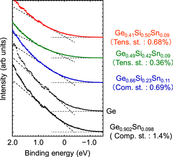
Figure 1. Valence band spectra of Ge1−x−ySixSny, Ge and Ge0.902Sn0.098 layers obtained by UPS. Also provided are the tensile (Tens. st.) and compressive strain values for each layer.
Download figure:
Standard image High-resolution imageFrom the valence band spectra shown in figure 1, we evaluated the valence band offset of Ge1−x−ySixSny and Ge for Ge0.902Sn0.098. Figure 2 shows the valence band offsets of various Ge1−x−ySixSny layers for Ge0.902Sn0.098 as a function of the Si content. The origin of the energy in figure 2 corresponds to the valence band edge of the Ge0.902Sn0.098 layer. The theoretical calculation results of the valence band offsets for the Ge1−x−ySixSny layers having strains of −1%, 0%, and 1%, respectively, are also plotted (dashed lines in figure 2), and we show the relationship between the Si and Sn contents (x and y) [21]. Considering another theoretical calculation report [22], the valence band offset in Ge0.902Sn0.908/Ge was estimated to be 106 meV, which is 10 meV larger than that evaluated from our experiment. This difference in the valence band offset values may be owing to strain in the Ge0.902Sn0.908 layer, where a compressive strain of −1.4% exists the Ge0.902Sn0.908 layer prepared in this study while the theoretical calculations do not consider the effect of strain in the Ge1−xSnx layer. Herein, as the Si content in Ge1−x−ySixSny increases, the valence band offset for Ge0.902Sn0.098 increases. This tendency corresponds to theoretically calculated predictions, and can be attributed to a lower valence band edge of Si than that of Ge [23]. However, the valence band offset between Ge0.902Sn0.098 and Ge1−x−ySixSny with a Si content of 23% was evaluated to be 100 meV and that between Ge0.902Sn0.098 and Ge was evaluated to be 96 meV. Considering the theoretical prediction shown in figure 2, this slight difference is related to a small Si content and compressive strain in Ge1−x−ySixSny, where the existence of the latter reduces the energy band offset. In contrast, in the sample with a Si content of 42%, the valence band offset was drastically increased compared with the 24%-Si case. We consider that this is not only owing to increasing Si content but also to the tensile strain in the Ge1−x−ySixSny layer. From the theoretical calculation [21] and our results, the reason of increasing the valence band offset can be attributed to two effects, one is a higher Si/Sn ratio and another is an effect of a large tensile strain in the Ge1−x−ySixSny epitaxial layer. The valence band offset between Ge0.902Sn0.098 and Ge1−x−ySixSny reaches a maximum with a Si content of 50%, and was evaluated to be 330 meV. This value is 13 times greater than the kBT value of 26 meV at room temperature and is sufficiently large for the confinement of holes in a Ge1−xSnx active layer at room temperature.
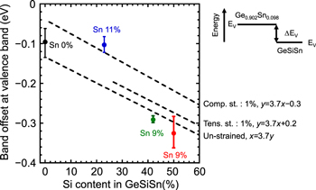
Figure 2. Valence band offset (ΔEV) between Ge0.902Sn0.098 and Ge1−x−ySixSny or Ge as a function of the Si content in the Ge1−x−ySixSny layer. Dashed lines represent the theoretical calculation results [21] for compressive (Comp. st.) and tensile (Tens. st.) strains and no strain (Un-strained).
Download figure:
Standard image High-resolution imageNext, we estimated the conduction band offsets of Ge1−x−ySixSny for Ge0.902Sn0.098 by calculating the bandgap of each layer based on the report of Ref. [21]. We estimated the conduction band edges of Ge1−x−ySixSny and Ge1−xSnx by adding the bandgap values calculated without considering the strain to the value of the valence band edge measured in this study. Figure 3 shows the summary of the energy band alignment of the Ge0.902Sn0.098/Ge1−x−ySixSny heterostructure as a function of the Si content of Ge1−x−ySixSny. The origin of the energy in figure 3 corresponds to the valence band edge of Ge0.902Sn0.098 and the valence and conduction band edges of Ge0.902Sn0.098 are plotted (dashed lines in figure 3). The measured valence band edges of the Ge1−x−ySixSny layers are lower than that of the Ge0.902Sn0.098 layer, and the estimated conduction band edges of the Ge1−x−ySixSny layers are larger than that of the Ge0.902Sn0.098 layer in all samples. This result indicates that type-I energy band alignment was achieved in all samples. Comparing the results of Ge1−x−ySixSny with a Si content of 23% and that with a Si content of 42%, there is no significant difference in the conduction band edge values. This result is attributed to a lower valence band edge in the Ge1−x−ySixSny with a Si content of 42%, as mentioned above, although its bandgap is larger than that of Ge1−x−ySixSny with a Si content of 23%. The conduction band offset of Ge1−x−ySixSny for Ge0.902Sn0.098 approaches its maximum when the Si content is increased to 50%, and was estimated to be 150 meV. This value is 5.7 times greater than the kBT value at room temperature. From these results of the valence and conduction band offsets, the Ge1−xSnx/Ge1−x−ySixSny heterostructure is preferable to achieve the type-I energy band alignment for the confinement structure of both holes and electrons in Ge1−xSnx active layer at room temperature.
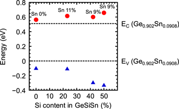
Figure 3. Energy band alignment of Ge0.902Sn0.098, Ge1−x−ySixSny and Ge as a function of the Si content in the Ge1−x−ySixSny layer. Conduction band edges (EC; red circles) were estimated by adding the bandgap calculated using the theoretical prediction of Ref. [21] to the valence band edges (EV; blue triangles).
Download figure:
Standard image High-resolution image3.2. Control of strain relaxation of Ge1−x−ySixSny epitaxial layers
In this section, we report the formation of strain-relaxed Ge1−x−ySixSny epitaxial layers for more preferable Ge1−x−ySixSny/Ge1−xSnx structures. First, we show the result of the Ge1−x−ySixSny layer grown directly on a p-Si(001) substrate. Figure 4(a) shows the XRD-2DRSM result around the reciprocal lattice point of Ge for the Ge0.71Si0.14Sn0.15/Si sample. XRD-2DRSM shows contour of the diffraction intensity and the vertical and diagonal lines in the reciprocal space map indicate the trajectories of the reciprocal lattice point of the pseudomorphic and the fully strain-relaxed Ge1−x−ySixSny, respectively. The diffraction peak related to the Ge0.71Si0.14Sn0.15 epitaxial layer is weak, which indicates that the crystalline quality of the epitaxial layer is poor. The Si and Sn contents were estimated from the comprehensive results of XRD-2DRSM and Raman scattering spectroscopy (not shown). Figure 4(b) shows an optical microscope image of the sample where a nonuniform surface can be observed, indicating that Sn precipitation takes place. From these results, it is evident that the epitaxial growth of a strain-relaxed Ge1−x−ySixSny layer directly on Si is fundamentally difficult. We deduce that the reason for this difficulty is primarily owing to the large lattice mismatch between Si and Ge0.71Si0.14Sn0.15. The lattice constant of Ge, Si, and Sn are 0.566, 0.543, and 0.649 nm [24], respectively, and that of the Ge0.71Si0.14Sn0.15 layer is estimated from Vegard's law to be 0.575 nm. Therefore, the lattice mismatch between Si and the Ge0.71Si0.14Sn0.15 layer is estimated to be 5.9% and this large lattice mismatch causes the degradation of the crystalline quality of the Ge1−x−ySixSny epitaxial layer during its growth on Si.

Figure 4. (a) Optical microscope image and (b) XRD-2DRSM result of the Ge0.71Si0.14Sn0.15 (50 nm) layer grown on Si substrate.
Download figure:
Standard image High-resolution imageTo improve the crystallinity of the strain-relaxed Ge1−x−ySixSny layer, we examined the effect of decreasing the lattice mismatch between the Ge1−x−ySixSny layer and the substrate by using a Ge(001) wafer and v-Ge as substrates, whose lattice constants are greater than Si. The XRD-2DRSM results around the reciprocal lattice point of Ge for the Ge0.64Si0.21Sn0.15/Ge and Ge0.61Si0.22Sn0.17/v-Ge samples are shown in figures 5(a) and (b), respectively. Optical microscope images of the Ge1−x−ySixSny layers grown on Ge and v-Ge substrates are shown in figures 5(c) and (d), respectively. The Ge1−x−ySixSny layer was prepared on each substrate using conditions similar to those mentioned above, and each element content was estimated comprehensively considering the results of XRD-2DRSM and Raman scattering spectroscopy. The surface morphologies of the Ge1−x−ySixSny layers grown on both the Ge and v-Ge substrates were uniform, unlike those grown on the Si substrate; thereby confirming the formation of uniform Ge1−x−ySixSny layers without Sn precipitation. The diffraction peak related to the Ge0.64Si0.21Sn0.15 layer grown on the Ge substrate is clearly observed at the same reciprocal-space value to the
 ![$[\overline{11}0]$](https://content.cld.iop.org/journals/0268-1242/32/10/104008/revision2/sstaa80ceieqn3.gif) direction (Qx) of the diffraction peak related to Ge. This indicates that the Ge0.64Si0.21Sn0.15 layer is pseudomorphically grown on the Ge substrate and that no strain relaxation of the epitaxial layer occurs. In contrast, the diffraction peak related to the Ge0.61Si0.22Sn0.17 layer grown on the v-Ge exhibited a smaller Qx value than that of v-Ge. This indicates that strain relaxation of the Ge0.61Si0.22Sn0.17 layer occurs, where the degree of strain relaxation (DSR) was estimated from the Qx value to be 55%. Interestingly, these results mean that the strain relaxation in a Ge1−x−ySixSny epitaxial layer preferentially occurs on a v-Ge substrate rather than on a Ge substrate, even with identical growth conditions.
direction (Qx) of the diffraction peak related to Ge. This indicates that the Ge0.64Si0.21Sn0.15 layer is pseudomorphically grown on the Ge substrate and that no strain relaxation of the epitaxial layer occurs. In contrast, the diffraction peak related to the Ge0.61Si0.22Sn0.17 layer grown on the v-Ge exhibited a smaller Qx value than that of v-Ge. This indicates that strain relaxation of the Ge0.61Si0.22Sn0.17 layer occurs, where the degree of strain relaxation (DSR) was estimated from the Qx value to be 55%. Interestingly, these results mean that the strain relaxation in a Ge1−x−ySixSny epitaxial layer preferentially occurs on a v-Ge substrate rather than on a Ge substrate, even with identical growth conditions.

Figure 5. XRD-2DRSM results around the reciprocal lattice point of Ge for the (a) Ge0.64Si0.21Sn0.15 (50 nm) layer grown on a Ge substrate and (b) Ge0.61Si0.22Sn0.17 (50 nm) layer grown on v-Ge. (c, d) Optical microscope images of the (c) Ge0.64Si0.21Sn0.15 layer grown on a Ge substrate and (d) Ge0.61Si0.22Sn0.17 layer grown on v-Ge.
Download figure:
Standard image High-resolution imageHere, we deduce the reason for this difference of the strain relaxation. Previously, our group has reported the enhancement of the strain relaxation of a Ge1−xSnx epitaxial layer on a v-Ge substrate owing to the threading dislocations that inherently exist in the Ge buffer layer [25]. The density of threading dislocations in the v-Ge substrate was typically estimated to be 1011 cm−2 in our previous case. We consider that a similar mechanism exists for the strain relaxation of the Ge1−x−ySixSny epitaxial layer on a v-Ge substrate in this study. The high-density threading dislocations in the v-Ge continuously propagate in the Ge1−x−ySixSny layer grown on a v-Ge substrate, and these threading dislocations should play the role of a nucleus generating the misfit dislocations at the Ge1−x−ySixSny/v-Ge interface. However, the crystallinity of the Ge substrate used in this study is very high and the density of threading dislocations on the Ge surface is negligible. In our case, the Ge1−x−ySixSny epitaxial layer pseudomorphically grown on the Ge substrate also exhibits high crystallinity and no threading dislocations are introduced in the growth of a thin epitaxial layer below the critical thickness of strain relaxation. As a result, it is considered that the strain relaxation in the Ge1−x−ySixSny epitaxial layer is enhanced with the propagation of misfit dislocations rather than that on Ge, even with the same growth conditions.
In addition, we examined the effects of enhancing the strain relaxation of Ge1−x−ySixSny layers by PDA to raise the in-plane lattice constant of the Ge1−x−ySixSny layer. Figure 6 shows the annealing temperature dependence of the in-plane lattice constant, the DSR of the Ge0.61Si0.22Sn0.17 layer, and the strain in the Ge0.94Sn0.06 layer, which would be formed on the Ge0.61Si0.22Sn0.17 layer as-grown or annealed at 300 and 400 °C for 10 min in N2 ambient. In figure 6, we estimated the strain in a Ge0.94Sn0.06 layer because the indirect-direct transition crossover of Ge1−xSnx is predicted with a low Sn content of 6% and a low tensile strain of 0.2% [19]. For comparison, we also show the results for the Ge0.64Si0.21Sn0.15 epitaxial layer grown on a Ge substrate. The DSR of the Ge0.64Si0.21Sn0.15 layer grown on a Ge substrate does not increase after 300 °C-PDA. After 400 °C-PDA, the DSR of the Ge0.64Si0.21Sn0.15 layer grown on a Ge substrate increases slightly, but the DSR value is as low as 7.5%. On the other hand, the DSR of the Ge0.61Si0.22Sn0.17 layer grown on v-Ge increases after PDA at 300 and 400 °C, and were estimated to be 64% and 70%, respectively. Notably, after 400 °C-PDA, the lattice constant of the Ge0.61Si0.22Sn0.17 layer was estimated to be 0.571 nm. This result indicates the possibility of the formation of a 0.14%-tensile-strained Ge0.94Sn0.06 layer on this Ge0.61Si0.22Sn0.17 layer, and a direct transition Ge1−xSnx layer could be obtained by increasing the strain relaxation slightly. Here, we deduce the reason for the enhancement of strain relaxation after PDA. In the Ge/Si case, there is a thermal expansion mismatch [26] whose influence on the strain should be considered. However, in the Ge1−x−ySixSny/Ge case, it is reported that the mismatch of the thermal expansion coefficient is negligibly small [27]. Also, in this study, the highest process temperature of 400 °C is not so high, therefore, we do not consider the effect of a thermal expansion mismatch upon the strain in epitaxial layer. From this reason, we think that the enhancement of strain relaxation only occurs due to the propagation of threading dislocations in the Ge1−x−ySixSny/Ge and v-Ge samples.

Figure 6. In-plane lattice constant (left axis) and DSR (right inner axis) of the Ge0.61Si0.22Sn0.17 layer grown on v-Ge, as well as the strain in the Ge0.94Sn0.06 layer (right outer axis) assumed to form on the Ge0.61Si0.22Sn0.17 layer as-grown and after PDA.
Download figure:
Standard image High-resolution imageWe also investigated the surface morphology of strain-relaxed Ge1−x−ySixSny layers using AFM observation, and figures 7(a) and (b) show the AFM images and surface profiles of the Ge0.64Si0.21Sn0.15/Ge and the Ge0.61Si0.22Sn0.17/v-Ge samples, respectively, after PDA at 400 °C. Scarcely any agglomeration can be observed on the surfaces of both samples, indicating that no Sn precipitation occurs after 400 °C-PDA. The root mean square (RMS) roughnesses of the Ge0.61Si0.22Sn0.17/v-Ge and the Ge0.64Si0.21Sn0.15/Ge samples were evaluated to be 2.7 and 4.7 nm, respectively, indicating that using v-Ge is an effective way to suppress the surface roughness.

Figure 7. AFM images (upper) and surface profiles (lower) of the (a) Ge0.64Si0.21Sn0.15 layer grown on a Ge substrate and (b) Ge0.61Si0.22Sn0.17 layer grown on v-Ge.
Download figure:
Standard image High-resolution image
4. Conclusions
We investigated the energy band alignment in Ge0.902Sn0.098/Ge1−x−ySixSny layers pseudomorphically grown on a Ge substrate. The measured valence band offset and the estimated conduction band offset, considering the energy bandgap of the Ge1−x−ySixSny layer, increased with the Si content in Ge1−x−ySixSny. The valence and conduction band offsets of 330 and 150 meV, respectively, were sufficient for both holes and electrons confinement in a Ge1−xSnx layer at room temperature in the Ge0.902Sn0.098/Ge0.41Si0.50Sn0.09 heterostructure.
In addition, we examined the formation of a strain-relaxed Ge1−x−ySixSny layer using a v-Ge substrate. The DSR of the Ge0.61Si0.22Sn0.17 layer grown on v-Ge was estimated to be as high as 55%, although that of the Ge0.64Si0.21Sn0.15 layer grown on a Ge substrate was 0%. We also examined the effect of PDA to enhance the strain relaxation. The DSR of the Ge0.61Si0.22Sn0.17 layer grown on v-Ge was increased to 70% after PDA at 400 °C. The surface roughness of the Ge1−x−ySixSny layer after 400 °C-PDA was sufficiently lowered by using a v-Ge substrate. We found that using v-Ge as a substrate was effective for both enhancing the strain relaxation and suppressing the surface roughness of the Ge1−x−ySixSny layer, even after PDA.
Acknowledgments
This work was partly supported by a Grant-in-Aid for Scientific Research (S) (Grant No. 26220605) from the Japan Society for the Promotion of Science (JSPS).