
Abstract
The silicon photomultiplier (SiPM) is an established device of choice for a variety of applications, e.g. in time of flight positron emission tomography (TOF-PET), lifetime fluorescence spectroscopy, distance measurements in LIDAR applications, astrophysics, quantum-cryptography and related applications as well as in high energy physics (HEP).
To fully utilize the exceptional performances of the SiPM, in particular its sensitivity down to single photon detection, the dynamic range and its intrinsically fast timing properties, a qualitative description and understanding of the main SiPM parameters and properties is necessary. These analyses consider the structure and the electrical model of a single photon avalanche diode (SPAD) and the integration in an array of SPADs, i.e. the SiPM. The discussion will include the front-end readout and the comparison between analog-SiPMs, where the array of SPADs is connected in parallel, and the digital SiPM, where each SPAD is read out and digitized by its own electronic channel.
For several applications a further complete phenomenological view on SiPMs is necessary, defining several SiPM intrinsic parameters, i.e. gain fluctuation, afterpulsing, excess noise, dark count rate, prompt and delayed optical crosstalk, single photon time resolution (SPTR), photon detection effieciency (PDE) etc. These qualities of SiPMs influence directly and indirectly the time and energy resolution, for example in PET and HEP. This complete overview of all parameters allows one to draw solid conclusions on how best performances can be achieved for the various needs of the different applications.
Export citation and abstract BibTeX RIS

Original content from this work may be used under the terms of the Creative Commons Attribution 3.0 license. Any further distribution of this work must maintain attribution to the author(s) and the title of the work, journal citation and DOI.
1. Introduction
The silicon photomultiplier (SiPM) (also solid-state photomultiplier, SSPM, or multi pixel photon counter, MPPC) is a solid state photodetector made of an array of hundreds or thousands of integrated single-photon avalanche diodes (SPADs), called microcells or pixels (Renker and Lorenz 2006, Renker and Lorenz 2009, Buzhan et al 2003, Golovin and Saveliev 2004, Herbert et al 2006). In analog SiPMs all cells are independent and connected to a common readout in parallel, with each cell having its own quenching resistor. Each cell is typically square with an edge length between 10 µm (Acerbi et al 2018a) and 100 µm (Wagadarikar et al 2013).
Upon the detection of a photon the SPAD generates a large electric output signal due to internal avalanche multiplication. In an SiPM it is possible to count each fired SPAD separately: (i) in a digital fashion (digital SiPM), where each SPAD is connected to its own readout electronics (Frach et al 2009, Liu et al 2016) or (ii) by the amplitude (or charge) of the sum of the single SPAD signals as in an analog SiPM (Renker and Lorenz 2006, Renker and Lorenz 2009, Corsi et al 2006). Either way, the SiPM allows one to detect and count photons with high resolution and with single-photon sensitivity (Renker and Lorenz 2006, Acerbi et al 2015, Buzhan et al 2009). The internal avalanche amplification is also fast enough to obtain very good timing information of the arrival time of the detected photons (Cova et al 1996, Acerbi et al 2014, Nemallapudi et al 2016), within several tens of picoseconds.
These properties, along with advantages such as low operation voltage, compactness and robustness, make the SiPM an excellent device for light detection from single photon to several thousand of photons, especially when fastest timing is a requisite. Typical applications based on low light intensity are light detection and ranging (LIDAR) (Agishev et al 2013, Acerbi et al 2018b), functional optical spectroscopy and fluorescent light detection in biology and physics (Mora et al 2015, Zimmermann et al 2013, Re et al 2016, Mik et al 2011). New arising and exciting fields can also be found in quantum physics (Kalashnikov and Krivitsky 2014) and quantum informatics (Balygin et al 2018). Coupled to organic or inorganic scintillators, SiPMs sense the scintillation light and/or Cherenkov light (Korpar et al 2011, Brunner et al 2014, Gundacker et al 2020) with highest time precision. They are used in nuclear medical imaging (Roncali and Cherry 2011, Lecomte 2009, Vinke et al 2009, Gundacker et al 2016a, Cates et al 2015), for gamma spectroscopy and for time tagging of high energetic particles (Herbert et al 2006, Benaglia et al 2016, Garutti 2011, Pauwels et al 2013). In these applications they exploit their higher granularity with respect to photomultiplier tubes (PMTs) and their insensitivity to magnetic fields. In oncological diagnostics time of flight (TOF) R&D in positron emission tomography (PET) was first studied in the 80's using fast emitting crystals, e.g. BaF2 or CsF. However, due to their low density the timing benefits were outweighted and they could not compete with high density crystals, e.g. Bi4Ge3O12 (BGO) (Moses 2003). The appearance of Lu2SiO5:Ce (LSO:Ce) or LaBr3:Ce around 2000 made it possible to resume TOF-PET research with PMT readout. Although, the real breakthrough was only achieved by the commercial availability of SiPMs which outperformed PMTs around 2010, mainly due to their higher photon detection efficiency (PDE) and better intrinsic timing properties.
New applications such as the search for dark matter or double beta decay demand novel developments of the SiPM to extend its PDE towards the vacuum ultraviolet (VUV) or deep ultraviolet (UV) (Gola et al 2019). On the other hand the already mentioned LIDAR market calls for a high PDE on the other side of the spectrum in the near infrared. Furthermore new challenges in TOF-PET, high energy physics (HEP), time resolved x-ray detection and spectroscopy push developments of the SiPM to achieve single photon time resolutions (SPTRs) as much as physically possible to the few picosecond domain.
The SiPM is an already established photodetector having entered many fields from basic scientific research to social and medical applications; however it is still a device with plenty of room for further developments. This paper will give an overview of the basics of an SiPM, in order to get a deep understanding of its working principles and main parameters. It begins with the description of the SPAD physics itself, the equivalent electrical model of SPADs and SiPMs followed by a definition of SiPM noise parameters, e.g. crosstalk, afterpulse, dark count rate, etc. In the second part of the paper the focus will be placed on SiPMs in selected applications such as time of flight positron emission tomography (TOF-PET) and in HEP.
2. The SPAD
The SPAD or Geiger mode avalanche diode (GM-APD) is the smallest building block or microcell of the SiPM. The SPAD exploits avalanche multiplication as an internal gain mechanism. The avalanche breakdown process has been studied in the '60s and '70s using avalanche photodiodes operated close to breakdown voltage or above (Haitz et al 1963, Haitz 1964, McIntyre 1961, Oldham et al 1972). The first avalanche photodiodes working above breakdown, in Geiger mode, have been proposed and studied in the '80s and '90s (McIntyre 1985, Cova et al 1989, Dautet et al 1993, Bondarenko et al 1998, Cova et al 1996). Currently, SPADs are realized in silicon, with custom or CMOS processes, with quenching and from case to case the readout circuitry in-pixel, or made in different materials, like III/V materials for near-infrared range detection (e.g. InGaAs) (Ting et al 2019).
In the following section the basic operational principles of a SPAD will be discussed together with the electrical equivalent model and an overview of characterizing parameters accessible to experimental evaluation will be given.
2.1. Principles of operation
A SPAD is essentially a p-n junction or diode, specifically designed to be biased in reverse direction above the breakdown voltage (Cova et al 1996, McIntyre 1985). Depending on the applied voltage there are three different regions of operation in such a photodetector. If the voltage is low, where no additional multiplication of the generated electron-hole (e-h) pairs is happening, the diode is operating in the photodiode regime (this is illustrated in figure 1(a)). An impinging photon can create one e-h pair, which is separated by the applied field and a current proportional to the light intensity can be measured. When increasing the applied reverse voltage on the diode, the electric field becomes so high that the electrons can gain enough energy to create secondary e-h pairs via impact ionization. This is the regime of the avalanche photodiode (APD). In the APD only the electrons can generate secondary e-h pairs, but not holes. The device shows a certain gain from several tens to hundreds and the measured current is proportional to the number of detected photons or generated e-h pairs. Because only electrons have enough kinetic energy to create additional e-h pairs, the avalanche only flows in one direction and is self quenched, i.e. no external circuit is necessary to stop the avalanche. This can be seen in figure 1(b).

Figure 1. (a) Operation regimes of solid state p-n junction, i.e. photodiode, avalanche photodiode (APD) and SPAD or SiPM range. (b) In the APD only electrons can sustain the avalanche, whereas in a SPAD holes will perform impact ionization as well. Reproduction from Otte (2007).
Download figure:
Standard image High-resolution imageIf the electric field or applied reverse voltage is increased even more, above the so-called breakdown voltage, holes will also gain enough velocity in order to create secondary e-h pairs (the reason that holes need more electric field to generate secondary particles lies in their higher effective mass). This is the regime of the SPAD used in SiPMs (illustrated in figure 1(a)). In such conditions, the electric field is high enough (in the order of a few 105  ) that a single carrier injected or generated into the depletion layer can trigger a self-sustaining avalanche process. The current increases very rapidly and the leading edge marks the arrival time of the detected photon with high precision. Subsequently the avalanche is quenched by lowering the bias voltage to or below the breakdown voltage, by a so called 'quenching circuit'. The bias voltage must then be restored in order to allow for the detection of another photon.
There are two ways of constructing a SPAD, either n-doped on p-doped or p-doped on n-doped, which can be seen in figure 2. Due to the reverse-biasing the generated electrons always flow in the direction of the n-doped connection. The avalanche triggering probabilty is the likelihood of an electron or hole passing the p-n junction to generate enough secondary e-h pairs in order to trigger a self-sustainable avalanche. This quantity is of course dependent on the SPAD structure and electric field, given by the applied bias voltage or excess bias. As already mentioned and illustrated in figure 3(a) (Oldham et al 1972), the avalanche triggering probability of electrons is higher than for holes. Hence, the avalanche is predominantly triggered by electrons, or in order to increase the PDE of the device electron avalanche triggering is preferred.
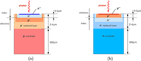
Figure 2. (a) The n-on-p SPAD structure is more sensitive in the red and (b) the p-on-n SPAD structure is more sensitive in the blue and near UV. Picture modified from Renker and Lorenz (2009).
Download figure:
Standard image High-resolution image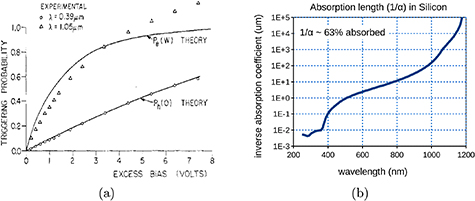
Figure 3. (a) The avalanche triggering probability of electrons and holes in a SPAD (reproduction from Oldham et al 1972). (b) Light absorption length in Silicon (data from Green and Keevers 1995).
Download figure:
Standard image High-resolution imagePhotons in the blue to UV are absorbed closer to the surface of the SPAD, which is illustrated in figure 3(b), showing the absorption length in silicon. This implies that in the case of the p-on-n structure blue light will predominantly generate electrons close to the surface, which will traverse the junction towards the n-doped region, connected to the positive pole of the bias voltage. Contrarily, light in the red with larger wavelengths will generate electron-holes deeper in the SPAD further away from the surface. In this case electrons are collected rather quickly traversing less material, giving them a lower chance of triggering an avalanche. The holes traversing the SPAD in the opposite direction, however, have a smaller avalanche triggering probability and, hence, the PDE for a p-on-n SPAD is lower in the red part of the spectra and higher in the blue. Consequently, a n-on-p SPAD is more sensitive in the red for light detection, because the above arguments are reversed. Of course in the design of a SPAD additional factors like the exact doping profile, drift regions, field distribution and junction depth will influence the final detection efficiency (Acerbi and Gundacker 2019).
2.2. Electrical equivalent circuit of the SPAD
The analog SPAD is esentially modeled as a parallel connection of the internal resistance of the diode space-charge region, i.e. Rd, and the inner depletion layer capacitance Cd, as can be seen in figure 4. The diode capacitance Cd can further be the sum of the SPAD area capacitance and any kind of perimeter or parasitic capacitances. Figure 4 also shows the integrated quenching circuit of an analog SPAD (Corsi et al 2006). The quenching circuit consists of the quenching resistor Rq and a parasitic capacitance Cq in parallel. Cq is responsible for a fast signal extraction (Acerbi et al 2014, Marano et al 2013), which can be beneficial, especially for fast timing applications, and is therefore a design parameter for optimal performance along with Rq.
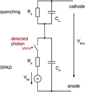
Figure 4. Equivalent electrical circuit of the SPAD with integrated quenching resistor.
Download figure:
Standard image High-resolution imageA triggered avalanche in the SPAD, either by a detected photon or noise event is modeled by closing the switch in figure 4 (Cova et al 1996, Marano et al 2014). This starts to discharge the capacitor Cd and provokes an exponential voltage drop at the internal node between Cq and Cd, initially being charged at the bias voltage of the SPAD applied between cathode and anode Vbias. It should be noted that upon closing the switch, the capacitance Cq is charging as well via Rd, provoking that the full charge involved in the recharging process is  and, hence, the voltage discharge time constant at the internal node given by
  (neglecting the influence of Rq, which usually is highly resistive). The voltage source in figure 4 is in most of the models set to the breakdown voltage Vbd, which gives the maximum voltage drop at the internal node being the bias voltage Vbias minus the breakdown voltage Vbd, i.e. the overvoltage
  .
.
The discharge of Cd and recharge of Cq is stopped when the current Id through Rd reaches a certain value, i.e. the 'threshold current', which is the minimum value of the current to get a self sustainable avalanche process. This value is a bit higher than the asymptotic minimum value Idf that Id would reach. This asymptotic current Idf is given by the overvoltage Vov divided by  (Seifert et al 2009), i.e.
  . Once the avalanche is quenched the cell recovery or recharge time is given by
  . Because the avalanche is quenched close to the asymptotic minimum value of Id the total charge which has to be provided from the outside via the SPAD anode and cathode is given by
  , which represents the SPAD gain multiplied by the electron charge.
In literature, the avalanche is sometimes modeled via a pulsed current source (Corsi et al 2006, Corsi et al 2007) in place of the series of the switch, the breakdown Vbd power supply and Rd (Seifert et al 2009). According to Thévenin's theorem both approaches are equivalent, however can simulate different angles of the problem. The current source can take into account the time structure of the avalanche development, whereas the model with the switch and Vbd source can describe the avalanche quenching or non-quenching.
2.3. Breakdown voltage and multiplication gain
As already discussed the reverse current-voltage curve shows a divergence at a certain bias voltage, the breakdown voltage (Vbd), at which the multiplication factor (M) (Kindt and Zeijl 1998) diverges. The multiplication factor is defined as the number of secondary carriers produced per each primary one. Above the breakdown voltage the photodetector works in Geiger mode and becomes a SPAD based detector. Besides the relatively high gain delivered by the Geiger mode operation and in fact defined by the quenching circuit, the real advantage lies in an almost gain independent excess noise factor, which is in contrast to an APD. The value of the breakdown voltage depends on the internal structure of the diode, i.e. the doping profiles at the p-n junction, and on the temperature.
Geiger discharge is reached when enough secondary (e-h) pairs are generated by impact ionization, in order to trigger a diverging avalanche process. Mathematically this can be described by the impact ionization rates αn and αp of electrons and holes, respectively, per unit distance. Together with the depletion region width W the breakdown voltage is reached when the ionization integral in equation (1) is equal to one (Maes et al 1990).

More sophisticated calculations of realistic structures are generally done within Technology Computer-Aided Design (TCAD) simulations, solving the Poisson equation along all trajectories. A general study of the breakdown voltage has been performed in (Serra et al 2011) and the following conclusions have been found: (1) Vbd increases with the thickness of the depletion region, (2) the temperature dependence of Vbd increases with the depletion region thickness and (3) in thin depletion regions the reproducibility of Vbd is higher. Hence, in view of optimizing the breakdown voltage it is more advantageous to work with thin depletion regions, which is possible if blue to UV light should be detected. Applications demanding red and infrared light detection, and therefore thicker depletion regions, might be more limited by breakdown uniformity and temperature stability.
The gain defined in equation (2) states the number of charge carriers collected per avalanche. In analog SPADs with integrated quenching resistors the gain is generally well defined due to a uniform production process of the internal capacitances Cq and Cd. If the quenching circuit is external, parasitic capacitances can have a significant influence and, hence, observed gain.

In equation (2), q is denoting the elementary charge q = 1.602 · 10−19 C. The gain is typically in the order of 105 to 107 (Piemonte et al 2016, Acerbi et al 2015) in analog SPADs and produces a single photon signal well above the electronic noise level, which gives the SPAD and SiPM excellent single photon counting capabilities (Buzhan et al 2009).
2.4. Dark count rate (DCR)
In silicon the primary dark count rate is due to the thermal generation of carriers by states in the bandgap and it can be modeled using Shockley–Read–Hall (SRH) statistics (Vincent et al 1979). This behavior is dependent on the temperature as 1/T and the dark current in silicon drops by a factor of 2 about every 10 °C. In SiPMs at room temperature the same behavior can be seen and the DCR increase and reduction versus temperature is equivalent with this factor. However, because of the high electric fields in SiPMs a saturation of the dark count reduction at low cryogenic temperatures due to trap assisted tunneling can be found, which is in contrast to other silicon photodetectors with gain one, e.g. PIN diodes. This tunneling effect dominates at low temperatures and is strongly dependent on the internal electric field strength. Figure 5 shows the DCR in two similar FBK NUV-HD SiPMs designed with a standard and low internal field structure at different overvoltages, demonstrating the tunneling electric field dependence (Acerbi et al 2017).

Figure 5. DCR for NUV-HD-SF (Standard Field) and NUV-HD-LF (Low Field) devices as a function of 1/T and overvoltage. Reproduction from Acerbi et al (2017).
Download figure:
Standard image High-resolution imageFor the dark count rate it is interesting to mention that only a small percentage of SPADs is responsible for the mostpart of the observed counts in an SiPM. In an analog SiPM the dark count rate can only be improved by better production processes and material pureness as all SPADs are connected in parallel. In the case of the digital SiPM it is thinkable to selectively switch off these 'screamer' SPADs in order to reduce the DCR (Mandai and Charbon 2012).
2.5. Afterpulse
Upon a primary event (dark count or detected photon) a secondary delayed event can be created with its amplitude or gain being lower than the primary event itself. This type of correlated noise is called afterpulse. The cause of afterpulse is the trapping and release of charge carriers in the high-field region. Deep and shallow traps are the mediators for afterpulsing with exponential release time characteristics. The afterpulse probabiltiy depends on the number of traps, release time constants and the recharge time of the SPAD. Thus, in order to reduce the afterpulse probabilty (or at least its visible effect), the recharge time constant can be tuned in order that most of the trapped charge carrier release happens when the cell is not yet (fully) recharged. Consequently a long SPAD recharge time generally reduces the afterpulse probability.
Afterpulse can be optically induced as well. During each avalanche secondary photons are produced (Gautam et al 1988). The amount has been estimated to 3 · 10−5 photons per avalanche carrier (Lacaita et al 1993, Otte 2009). These photons can be re-absorbed in the same SPAD in the neutral region. The generated charge carriers can diffuse to the high field region triggering an avalanche. In the substrate the carrier release time can be between a few nanoseconds to hundreds of nanoseconds (Acerbi et al 2015). The afterpulse probability can be reduced by carefully selecting the material, like using a low-lifetime substrate.
3. The analog SiPM
In order to keep the dark count rate low and the signal response of the SPAD fast, its dimensions should be lower than ∼100 µm. Additionally a single SPAD shows a certain dead time after being fired. In order to build a useable photodetector it is necessary to combine many SPADs to an SiPM. In the case of the analog SiPM the SPADs are connected in parallel, as can be seen in figure 6. If one SPAD is firing a certain output signal is recorded, if two SPADS are triggered at the same time two similar signals overlap and form a signal with double the amplitude and so on. In this sense the analog SiPM allows one to count the number of SPADs fired by integrating the charge in time, which is proportional to the number of photons detected (as long as the number of photons detected is smaller than the total amount of SPADs available). Presently the trend is to produce SiPMs with very small SPADs in the  range in order to increase the dynamic range.
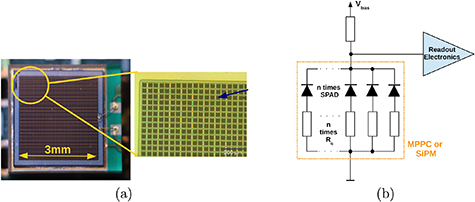
Figure 6. (a) Picture of an analog SiPM (HPK S10931-3050P) with zoom on the individual SPADs (indicated by the arrow). (b) In an analog SiPM all SPADs with integrated quenching resistor are connected in parallel.
Download figure:
Standard image High-resolution image3.1. Electrical equivalent circuit of the analog SiPM
As already discussed, the analog silicon photomultiplier (SiPM) is an array of SPADs connected in parallel. In the electrical equivalent model (seen in figure 7) the differences in the SPAD equivalent circuit are the additional passive components of the other not-triggered SPADs plus the grid inductances and capacitances (Corsi et al 2006, Marano et al 2014, Seifert et al 2009). For single photon detection these additionally not triggered cells add up to a non-negligible (several 100 pF) capacitance on the input of the amplifier electronics, which depending on the bandwidth and readout-scheme can change the single SPAD signal to a large extent.
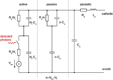
Figure 7. Equivalent electrical circuit of the SiPM. Switch represents the avalanche ignition, whereas the diode series resistance is given by Rd, the diode capacitance by Cd , the quenching part by Rq and Cq. The non-active not triggered cells are represented in the passive part and the parasitic part shown as series and parallel parasitic components. Nf denotes the number of simultaneously fired SPADs and  is the total number of SPADs in the SiPM.
Download figure:
Standard image High-resolution imageAn avalanche in one SPAD provokes that Cd is discharging via Rd, which leads to a voltage drop across Cq inducing a current which is charging Cq via Rd. This external current has to be provided from the outside and is proportional to the gain of the SPAD. However, the fast high-frequency part of this current initially is provided from the capacitance of the many inactive cells, which depending on the front-end electronic design can either reduce the signal amplitude or the speed of the signal, as briefly discussed below.
Depending on the SiPM readout, in "voltage" or "current" mode, different frequency behaviors of the sensed signal can be observed. For example, sensing only the voltage drop between anode and cathode of the SiPM leads always to a fast signal component mediated via Cq. However, the charge of this signal is divided between the large parasitic capacitance of the inactive cells and the small Cq, hence, for larger SiPMs the fast voltage signal amplitude is reduced by the ratio of the capacitances (capacitive divider). Still, the signal speed remains constant for large SiPMs. On the other hand if one has a transimpedance amplifier ("current mode") the input impedance will play a crucial role. If the input impedance of the amplifier is not low enough then the impedance of the parasitics of the SiPM and inactive cells will filter the high-frequency part of the signal, smearing it in time. Even so, by measuring the current an integration of the whole signal in time will always give similar (gain) values independent of the SiPM size. In a real system, however, both readout modalities are always present. Hence, the exact front-end design is a crucial input parameter for any simulations, e.g. in SPICE, in order to understand the measured SiPM signals.
In the frequency domain the absolute impedance of the SiPM can be obtained as in equation (3), if no SPAD is firing. This function can serve to estimate the SiPM's equivalent circuit component values by measuring  in the frequency range and fitting to the model (Scheuch et al 2015).

 (also called
  ) is the admittance of the single cell, which is then multiplied by the total number of pixels in the
  calculation, since they are all supposed inactive. For intermediate frequencies
  is dominated by Cd. The capacitive component of
  is
is  . At high frequencies the contribution of Cq dominates over the Rq one, thus the capacitive component of
  is
is  .
.
Because of epitaxial layer depletion, the impedance will depend on the absolute voltage applied to the SiPM. The smaller depletion at low bias will give a higher Cd, whereas a progressively higher depletion reaching the breakdown voltage will lower the value of Cd. The change of depletion region thickness is relevant above breakdown also, a small dependence of the measured impedance on the overvoltage will occur, even though a direct impedance measurement above breakdown is generally difficult. Moreover, a change in the equivalent circuit as a function of the number of pixels firing can be seen, leading to a slight change in the output signal (due to different load and charge partitioning).
Neglecting the parasitic part in equation (3) the complex impedance Z(ω), or the complex admittance Y(ω), can be rewritten as in equation (5) (Seifert et al 2009), further assuming that no cells in the SiPM are firing.
where G(ω) and C(ω) are the measurable parallel conductance and capacitance of the SiPM, which can be obtained with a precision LCR meter. Equation (5) can be solved to obtain the solution for Cd and Cg from G(ω) and C(ω), as can be seen in equations (6) and (7), respectively.

The sum  can be measured via the gain of the SiPM,
  and the quench resistor value Rq can be obtained from the forward current measurements, knowing the number of cells in the SiPM (
 ). This defines all parameters of the SiPM equivalent model except the diode series resistance Rd, which in theory could be estimated by the single SPAD signal rise time. However, other effects such as bandwidth limitations of the used electronics and parasitic inductances makes the direct measurement of Rd via the signal rise time unreliable. In most of the cases, however, Rd can be assumed to be small in the range of
  and simulations show that changing Rd in a broad range does not impact the model output too much (Seifert et al 2009).
3.2. IV curve and breakdown voltage determination
The breakdown voltage (Vbd) is one of the most important parameters of the SiPM, because the gain, PDE and other parameters are best specified versus the overvoltage applied to the SiPM. There are two ways of defining Vbd. The first method that is widely used is to measure the gain from the first photoelectron peak in the pulse height spectrum as a function of the bias voltage. In this method the Vbd is then found by extrapolating the gain to zero (Acerbi and Gundacker 2019, Klanner 2019).
In the second method, the maximum of the derivative is used (Musienko 2014) to find at which bias voltage the Geiger mode (or SPAD breakdown) starts. To get sufficient accuracy with this method it is sometimes necessary to inject some light into the SiPM. This is especially the case if small SiPMs or SiPMs with low gain and low dark count rate are to be measured. Figure 8(a) shows the IV curve of the SiPM under illumination of different constant current biased LEDs. In figure 8(b) the calculated derivative where the measured Vbd is independent of the LED intensity is shown. Further, it can be seen that only limited accuracy of the measurement was reached with very low external light intensity (LED1). The IV breakdown determination gives in general slightly larger values of maximum 0.5 V higher as compared to the method determining the breakdown by extrapolating the SPAD gain to zero. In our opinion the IV method is more correct, because in reality the gain at Vbd is not really zero since the SiPM already has a small avalanche gain before the Geiger mode starts (avalanche photodiode regime). An additional advantage of the IV method is that it can be easily obtained, and in general measurement of the IV characteristic is fast and applicable for device monitoring in the production process.

Figure 8. (a) IV characteristic of an SiPM illuminated with various intensities of an external LED. (b) The derivative of the IV curve versus applied bias voltage for the various intensities of the LED.
Download figure:
Standard image High-resolution image3.3. Prompt, delayed and external crosstalk
A summary plot of the various noise types is given in figure 9, represented by their observable analog waveforms. The plot shows the primary noise source of an SiPM; the dark count rate (DCR), which is indistinguishable from detected photons. Corellated noise sources are afterpulsing, prompt-, delayed- and external-crosstalk. The term correlated noise indicates that this type of noise is a follow-up process of a primary event, i.e. an avalanche triggered either caused by a thermally generated (e-h) pair (DCR) or caused by a detected photon.

Figure 9. Representation of the SiPM output signal on the different kinds of noise observable: primary events, prompt crosstalk, afterpulsing and delayed crosstalk events. Reproduction from Acerbi and Gundacker, (2019).
Download figure:
Standard image High-resolution imageAs already mentioned, each avalanche in a SPAD produces optical photons due to hot-intraband luminescence (Lacaita et al 1993). These photons can traverse to a neighboring SPAD and trigger an avalanche giving rise to prompt or direct crosstalk, as is shown on the very left in figure 10. The direct crosstalk probability has its peak value when the primary avalanche has reached roughly its maximum of produced e-h pairs. According to a study of the avalanche process in SPADs (Ingargiola et al 2011) this happens some hundreds of picoseconds after the initial event. Due to the small distance the light has to travel, prompt crosstalk is timed very close to the primary event, starting from almost no time delay to a delay of, at maximum, several hundreds of picoseconds.
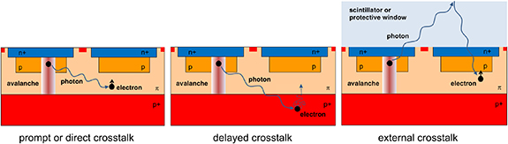
Figure 10. Different types of crosstalk observable in analog SiPMs. Reprint from Piemonte and Gola (2019).
Download figure:
Standard image High-resolution imageDelayed crosstalk or delayed optical crosstalk is generated by secondary avalanche photons, which are absorbed in the un-depleted region of a neighboring SPAD (see figure 10, middle). These photon-generated minority carriers can reach the multiplication region of the SPAD by diffusion and trigger an avalanche. The carrier diffusion time can be quite long and the delays are generally long enough that the delayed crosstalk events can be separated from the primary events. However, part of the delayed crosstalk events will occur too shortly following the first avalanche in which case this type of noise is not distinguishable from prompt crosstalk. It should be mentioned that delayed afterpulsing might lead to the same type of signal at the SiPM terminal as delayed crosstalk, this especially if the SPAD of the afterpulse event was almost or already fully charged. Since the thickness of the superficial un-depleted region of the entrance window is normally very small, it can be assumed that the most important contribution to the delayed crosstalk comes from the region below the active area (Piemonte and Gola 2019).
Another type of crosstalk is of external nature, as can be seen in figure 10 (right hand side). Because the optical photons generated by the primary avalanche are isotropic, a good part will exit via the active side of the SiPM. A protective glass window or epoxy resin will reflect a part of these photons back to the SPADs via total internal reflection, generating external crosstalk. The secondary avalanches are not restrained to neighboring SPADs anymore and the external crosstalk probability might exceed the other sources of crosstalk. In fact, by coupling a crystal wrapped in reflective material on top of the SiPM (like in PET applications) this type of correlated noise can even limit the operational range of an SiPM, as can be seen in figure 11 (Gola et al 2014), where the 'second breakdown' is defining the maximum SiPM bias voltage applicable for stable operation. It can be seen that this value is around 11 V overvoltage in the case of a cleaned SiPM, without protective resin on top of the active area. Gluing a scintillator on top of the NUV device produced at Fondazione Bruno Kessler (FBK), used in this study, reduces the maximum applicable overvoltage to about 7 V. This behavior has also been described in other publications (Nemallapudi et al 2015, Gundacker et al 2016a).

Figure 11. Reverse bias currents measured at different temperatures with and without scintillators of different lengths coupled to the SiPM via optical glue. Reprint from Gola et al (2014).
Download figure:
Standard image High-resolution imageA way to reduce prompt crosstalk is to indroduce optical trenches in-between the cells. Delayed crosstalk can be minimized by reducing the un-depleted region thickness, using a substrate with a low minority carrier lifetime (Acerbi et al 2015), a buried junction below the active area to prevent diffusion or by extending the trenches deep into the subtrate to confine the optical photons within the same SPAD. Crosstalk in general and in particular external crosstalk can be minimized by reducing the SPAD gain, which will reduce the produced e-h pairs and, hence, the generated hot-intraband optical photons. Indeed, current research is moving in the direction of reducing the SPAD size down to sizes of 15µm and smaller, which reduces the SPAD gain, increases the SiPM dynamic range and shows advantages in radiation hardness.
3.4. Excess noise factor (ENF)
For an ideal photodetector the energy and time resolution is limited by pure photo-statistics. Meaning that for the real number of photoelectrons  (primary SPADs triggered by the incoming photons) created the event to event fluctuations are given by the standard deviation or root mean square (rms) and is equal to the
  . However, the non ideal characteristics of the SiPM, like the inter SPAD crosstalk and integrated afterpulsing will contribute and increase the signal. Hence, by measuring the mean charge or pulse height distribution and dividing it by the SPAD gain one will get a larger value than the real
  . This is often referred to as excess charge factor (Klanner 2019):
where  is the average total charge measured and
  is the average charge of the primary photoelectrons. Since this excess charge from crosstalk and afterpulsing appears as an artificial gain in the system the resolution of the pure primary Poisson-statistics is degraded and is referred to as the excess noise factor:

where σQ is the rms of the charge distribution in the measured spectrum and  the average total charge. Further
  and
and  represent the rms fluctuation and average charge of the primary photoelectrons. Since the crosstalk and afterpulsing are strongly dependent on the internal electric field strength in practice the ENF is unity around the breakdown voltage and increases with the overvoltage. Very successful R&D on trench technology to optically isolate the SPADs has been done to decrease the crosstalk to create SiPMs for high resolution detectors. The best low crosstalk SiPMs have almost unity ENF up to 5 V overvoltage. As previously mentioned, the SPAD crosstalk is also dependent on the reflections on the top surface. So if an epoxy layer or other reflecting medium, like a scintillating crystal wrapped in reflective material, is placed on top of the SiPM it can increase the ENF significantly.
3.5. SiPM saturation and non-linearity
In applications where one expects large signals, the limited number of SPADs in an SiPM causes saturation of the signal. The first commercial SiPMs had a limited SPAD size of minimum 50 µm to 100 µm, but in the last years much smaller SPAD sizes (down to 10 µm) are greatly improving the linear range. However, with very small SPAD sizes the relative dead space between SPADs increases, which decreases the PDE. So a trade off needs to be made between PDE and linear range. The general equation for the number of triggered SPADs ( ) as a function of the number of photons (
 ) and total number of SPADs in the SiPM (
 ) based on the statistical process on a uniform illumination of the SiPM can be given by equation (10) (Renker and Lorenz 2009, Grodzicka-Kobylka et al 2019).

Respective plots and measurements of various SiPMs can be found in Gruber et al (2014), which describes 'over-saturation' effects of some devices as well. Similar effects and complete phenomenological parametrizations can be found in Bretz et al (2016). Nevertheless, in most applications the light source does not illuminate the SiPM completely uniformly and a good simulation or measurement needs to be made in order to calculate the correction factors accurately. In addition, the situation gets more complex if the light source has a larger decay time than the SiPM recovery time, causing the cells to be able to be triggered multiple times within the same light pulse (Vinogradov et al 2011, Grodzicka-Kobylka et al 2019). As a consequence the linear range using small SPAD sizes is also increased by the shorter recovery time due to the lower capacitance of the smaller SPADs ( ).
).
3.6. PDE
In almost every application of SiPMs it is important to optimize the PDE and there are many different SiPMs available for use from the UV to the infrared (IR). The PDE quantifies the ability of a single-photon detector to detect photons. This is the ratio between the number of detected photons and the photons arriving at the detector. The general formula for the PDE of the SiPM is given in equation (11).

Here QE is the quantum efficiency, PT the avalanche triggering probability, Vov is the overvoltage and  is the effective geometrical fill-factor. The QE of silicon is dependent on the wavelength λ and for UV applications manufacturers have to use special protective coatings to optimize the QE in the UV.
The fill factor or also called geometric factor is defined as the active area of all SPADs divided by the total area of the SiPM. The inactive area is created in order to separate the SPADs electrically and optically from each other. For the bigger SPAD sizes of 50 × 50 µm2 the fill factor can be as large as 80% where for the smallest cell sizes of  it is limited to 30%. As the fill factor is linked mostly to the SPAD size the linear range required in the application needs to be taken into account. It is worth mentioning that the best fill factor in modern small size SPAD SiPMs is attained using transparent metal film quenching resistors (MFQR) versus the more standard option of a non transparent Polysilicon quenching resistor which can also be responsible for more dead space. The geometric fill factor is typically not included in the PDE calculation when characterizing a single SPAD, in this case the photon detection probability PDP is quoted.
The Geiger mode probability or avalanche trigger probability is a function of the overvoltage and the wavelength of the incoming photons. The ionization rate is higher for the electrons than for the holes and it is therefore much more efficient to collect the electrons than the holes for each e-h pair generated by an incoming photon. Because the absorption depth in silicon is growing with the wavelength, about 10 nm in the UV to 10th of microns in the visible range, it will depend on the SPAD structure if the holes or electrons are most efficiently collected.
There are two kind of structures illustrated in figure 12, where the authors in Piemonte and Gola (2019) plot the electron and hole Geiger probability versus the two widely used SiPM structures called n+ on p and p+ on n. Generally for wavelengths above 500 nm the n+ on p structure will have a superior PDE and for wavelength below 500 nm one does better using a p+ on n structure.

Figure 12. Electric field and triggering probability for two structures: n+/p and p+/n. Junction is highlighted with a dashed line. Reproduction from Piemonte and Gola (2019).
Download figure:
Standard image High-resolution imageBecause the electric field over the junction increases with the overvoltage the PDE will increase quickly and usually saturates around 5–7 V overvoltage. Of course by increasing the overvoltage the dark count rate (DCR) will also increase, so an optimum can be found which is usually also dependent on the amplifier noise.
To measure the PDE special attention has to be given to correlated noise sources in SiPMs, i.e. the crosstalk, afterpulse and dark count rate (Eckert et al 2010, Zappala et al 2016, Otte et al 2006, Otte et al 2017). Upon the detection of one impinging photon the measured output signal can be caused by either a real single SPAD firing or a multiple of the single SPAD signal due to correlated noise. One method, in order to avoid a bias of the PDE measurement by crosstalk or afterpulsing, is to exploit Poisson statistics. By measuring the ratio of how many times there was no photon detected (zero or pedestal events)  to the total amount of events
  , the mean number of photoelectrons detected
  can be expressed, as in equation (12) (Eckert et al 2010). Additionally, a dark scan with no light ilumination has to be performed in order to correct for possible dark count events in the integration window
  and
and  .
.
Presently many SiPM producers reach very high and comparable PDE values up to 60% (figure 13). The evolution in PDE made by FBK and HPK is summarized in figure 14, showing the advancements of devices from 2010 until 2018. Two main reasons for the seen increase in PDE have been: (1) a better geometric fill factor by reducing the dead-space between the SPADs (better lithographic processes) and (2) a reduction in optical crosstalk and afterpulse, which made it possible to operate the SiPMs at higher overvoltages boosting the avalanche triggering probability by a higher electric field. Further, operating at higher overvoltages the effective fill factor will be slightly increased due to the electric field saturating in a larger area of the SPAD, especially at the edges.

Figure 13. PDE as a function of the SiPM overvoltage measured at 410 nm. (a) Hamamatsu S13360 and S14160 with a picuture inset of HPK S14160 showing the center wire-bond connection, leading to a slight loss of PDE (SPAD pitch is 50 µm) and better SPTR. (b) Comparison of the PDE for Broadcom, FBK, Ketek and SensL (part of ON-semiconductors). Reproduction from Gundacker et al (2020).
Download figure:
Standard image High-resolution image
Figure 14. Progress made in SiPM photon detection efficiency by FBK and HPK. (a) PDE measured at 410 nm for FBK near UV (NUV) devices. (b) PDE measured at 410 nm for HPK devices.
Download figure:
Standard image High-resolution image3.7. Single photon time resolution (SPTR)
With the maturity of SiPMs in many aspects the SPTR is one of the few parameters which can still show major improvements. This is especially important for applications like TOF-PET, Cherenkov radiation detection, LIDAR and time correlated single photon counting setups. Especially in the case of analog SiPMs, the front-end readout, bandwidth and electronic noise play a crucial role in achieving the intrinsic SPTR limits imposed by the SiPM itself. This can be understood by the well know equation (13), expressing the part of the single photon time resolution (SPTR) only caused by the electronic readout with  the rms of the electronic noise floor and
  the slew rate of the signal at a given leading edge threshold level (Nemallapudi et al 2016, Gundacker et al 2020). It can be seen that a low noise amplifier and/or a faster signal with a fast rise time (higher bandwidth) can lead to improved timing behavior.

Recently, major achievements have been accomplished using high-frequency electronics, making use of the fast signal mediated via the SPAD quenching capacitance. SPTR values as low as 90 ps FWHM have been measured illuminating an FBK NUV-HD SiPM uniformly with a picosecond-laser (Cates et al 2018), by subtracting the picosecond laser pulse width of 42 ps FWHM a value of 80 ps FWHM was measured. Nevertheless, even in this case with optimized electronics the real intrinsic SiPM SPTR was shown to be 70 ps FWHM by estimating and subtracting the influence of the front-end electronic noise (according to equation (13)). Indeed different producers show very different performance regarding the SPTR, as can be seen in figure 15. This is mainly explained by different SPAD technologies and the different interconnection schemes between the SPADs applied by the various producers. Furthermore, up until now it was difficult to measure the intrinsic SPTR performance of SiPMs, which made targeted improvements difficult, which is in contrast to the PDE, DCR, afterpulse and crosstalk for example.
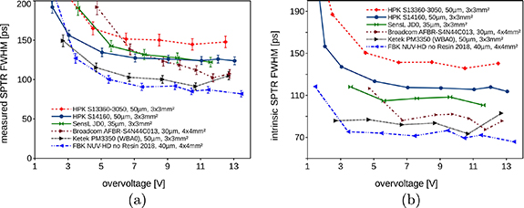
Figure 15. Measured single photon time resolution of HPK, SensL, Broadcom Ketek and FBK. (a) Measured SPTR of the various SiPM producers tested, including the picosecond laser pulse width and electronic noise. Measured SPTR values are always given illuminating uniformly the whole active SiPM area. (b) Intrinsic SPTR of the various SiPMs: electronic noise contribution and laser pulse width of 42ps FWHM is quadratically subtracted. Reproduced from Gundacker et al (2020).
Download figure:
Standard image High-resolution image3.8. Temperature dependence of SiPM parameters
The breakdown voltage of the SiPM is temperature dependent, because the mean free path for electrons decreases with increasing temperature, hence a higher electric field is required to start the avalanche process. Since the gain is only dependent on the cell capacitance and the applied overvoltage, the gain of the SiPM increases by lowering the temperature due to the breakdown voltage shift, i.e. effectively the overvoltage is increased. For different SiPMs we find different breakdown voltage shifts depending on their junction thickness. For shallow junctions with a depletion voltage of only 25 V this shift is in the order of 20 mV/°C, where for wider junctions with a depletion voltage of 75 V this parameter is in the order of 60 mV/°C. In applications where it is not convenient to stabilize the temperature itself it is possible to stabilize the overvoltage by using this coefficient with a feedback loop to a simple temperature sensor.
Another parameter strongly dependent on the temperature is Shockley–Read–Hall (SRH) induced dark counts as discussed in chapter 2.4. Lowering the temperature can effectively lower the DCR until the point where tunneling overtakes.
Other parameters as the SPTR, PDE or crosstalk probability are more or less stable with temperature as long as the overvoltage is fixed. Especially in commercial applications like PET, LIDAR in automotive or in spectroscopy, temperature ranges are commonly not exceeding the −40 °C to 85 °C range and therefore secondary effects on PDE, SPTR and other factors which can be observed at very extreme temperatures are not an issue. However, it should be mentioned that if the quenching resistor is made out of polysilicon the resisitive value can change with temperature, which then can be the cause of a changed signal shape and even manifest in a non-proper avalanche quenching at high overvoltages and certain temperatures.
3.9. Electronic readout of SiPMs
There are several approaches to reading the signal of analog-SiPMs, all of them having their advantages and disadvantages. Typically the readout electronic has to cope with the remarkably high terminal capacitance of the SiPM and its high overal gain, which is very unevenly distributed in time. As already mentioned a fast component of the signal is almost immediately transfered to the SiPM output via the quenching capacitance Cq, only mediating a small part of the overal gain. The rest of the gain is delivered via the quenching resistor Rq (recovery of the cell) with a time constant  . In view of integrating the front-end in ASICs with several tens to hundreds of channels and further to PET or HEP systems with thousand of channels, the power consumption plays a crucial role for the electronics design. Limiting the power consumption inevitably sets compromises on the best achievable performances and also on the readout architecture.
An overview of the SiPM timing characteristics with coupled front-end electronics can be given by considering the SiPM equivalent circuit in figure 7, neglecting the parasitic inductance  and resistance
  . By connecting the front-end input and its characteristic resistance
  between the cathode and anode of the SiPM it can be derived that the fast part of the input voltage transient seen by the preamplifier (the voltage over
  ) is equal to equation (14) (Calò et al 2019).

With  being the fraction of the total charge
  provided via the quenching capacitor Cq. Considering the value of
  being sufficiently low, commonly the case for SiPM readout, the time constant
  . The term
  is the equivalent capacitance of the detector at high frequencies, given by
  . In practice equation (14) states that the fraction of the charge flowing over Cq is almost immediately collected on the high frequency equivalent capacitance of the detector
  and then discharged via the amplifier input impedance
  . In this respect the fast component of an SiPM is in its speed basically only limited by the bandwidth of the amplifier and the avalanche growth in time itself. Indeed rise times of the single SPAD signal below 700 ps (10–90% of the SPAD amplitude) have been measured with amplifiers of 1.5 GHz using FBK SiPMs of
  size (Gundacker et al 2020). It can be further stated that the input capacitance of the amplifier
  does not play a significant role, as usually
  is much higher. Equation (14) also shows that a higher device capacitance (bigger SiPM area) immediately lowers the fast signal amplitude, which is unfavourable for fast timing. This is because it lowers the signal to noise ratio on the leading edge, according to equation (13), if one assumes that the electronic noise floor of the amplifier is not changing significantly. A further analysis of the slow recharging component can be found in Calò et al (2019), with the conclusion that the slow component, not very useful for fast timing, indeed becomes faster and larger in voltage amplitude if the input resistance
  is decreased.
Sensing the current flowing through  a lower value of the input impedance would lead to a higher current spike according to equation (14), because the voltage jump is basically defined only by the ratio of capacitances. Qualitatively it could be stated that, if the input impedance of the front-end electronics is much lower compared to the passive terminal capacitance of the SiPM, at a given frequency, all the signal at this frequency is extracted. Then, in principle, the signal remains the same for large or small SiPM active areas. However, considering an SiPM capacitance of 1 nF and 1
  front-end input impedance of a current mode amplifier, this would mean in first order approximation a
  bandwidth of 159 MHz, only. And, hence, the above argument renders only true for lower frequencies. In this case, the integrated charge flowing into the front-end would remain the same for a large or a small SiPM, consistent with an equal SPAD gain. But the large SiPM terminal capacitance will lower the bandwidth of the signal, and therefore the fast signal mediated via Cq will deteriorate, i.e. the signal rise time becoming slower and amplitude becoming smaller. On the other hand, in the case of a voltage amplifier, monitoring the voltage drop across the anode and cathode, bandwidths of 1 GHz and higher are easily possible. Nevertheless, the draw-back of this readout scheme is a very low voltage amplitude for large SiPMs with high passive terminal capacitance.
As previously introduced, in view of achieving good timing performance with SiPMs two front-end approaches are normally used (illustrated in figure 16), i.e. the voltage or current mode amplifier (Calò et al 2019). It should be mentioned as well that charge sensitive amplifiers could be used to read the signal from SiPMs, however, this has limitations in achieving good time resolution due to the high SiPM terminal capacitance. Still, due to the very good noise performance of charge amplifiers, a possible application of this type of amplifier could be using low gain SiPMs with small total equivalent capacitance (small cell size and small active area), especially if timing accuracy is not the most important parameter.
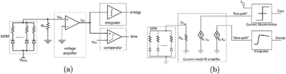
Figure 16. The two main modes of reading the analog SiPM signal, (a) voltage mode approach and (b) current mode approach. Reproduction from Calò et al (2019).
Download figure:
Standard image High-resolution imageASICs applying a voltage readout approach are for example SPIROC (Lorenzo et al 2013), EASIROC (Callier et al 2012), PETIROC (Fleury et al 2014) and PETA (Fischer et al 2009, Piemonte et al 2013). Using a voltage mode approach excellent timing can be achieved by using monolithic microwave integrated circuit (MMIC) radiofrequency (RF) amplifiers, commonly used for telecommunication. Designs such as this are explained in Yeom et al (2013), Cates et al (2018), Gundacker et al (2019). An interesting concept is to use a balun tranformer to adapt the balanced SiPM signal to the unbalanced input of the amplifier (Cates et al 2018) which gives the additional advantage of suppressing common ground noise effectively, similar to a differential readout of the SiPM, e.g. as in the PETA chip or NINO ASIC (Anghinolfi et al 2004).
Examples of ASICS using a current readout approach are the NINO ASIC (Powolny et al 2011, Anghinolfi et al 2004), STiC3 (Stankova et al 2015), FlexTOT (Comerma et al 2013, Sarasola et al 2017) and TOFPET2 (Francesco et al 2016).
4. The digital SiPM
In the preceding chapters, most of the focus was placed on the analog SiPM. This is mainly due to its predominance in appliations, e.g. PET or HEP, because of its mature production processes with high yield, achieving low dark count rates, high PDE and attractive costs. Nonetheless, on the hunt for the perfect photodetector the digital-SiPM might be the ultimate winner. In the fully digital or multi-digital SiPM each SPAD is connected to its own readout electronics (shown in figure 17(a)), including front-end and digitization of the signal's time stamp via a time to digital converter (TDC) (Frach et al 2009, Mandai and Charbon 2012). Such a detector would give the full time information of a detected light pulse, e.g. from a scintillating crystal.
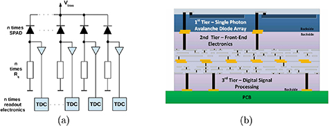
Figure 17. (a) Basic sketch of the multi-digital SiPM. Each SPAD is connected to its own quenching circuit and readout electronics. Reproduction from Gundacker et al (2015). (b) State-of-the-art research moves in the direction of 3D assembling of the digital SiPM. With customized produced standard SPAD arrays and through-silicon-via bonded electronics below or back-side illuminated SPAD arrays with connected electronics on the sensor 'front' side. An example is the 3D integrated single photon counting module (3DSPCM) under development by the Sherbrooke group (Bérubé et al 2015).
Download figure:
Standard image High-resolution imageThe first commercial digital SiPM was introduced by Philips (Frach et al 2009, Haemisch et al 2012). This device was specially designed to sense the light pulse of scintillating crystals for TOF-PET but was also successfully used to detect Cherenkov radiation in PET and HEP (Brunner and Schaart 2017, Frach 2012). The Philips d-SiPM records only one time stamp per scintillation event, which can be set on different probabilistic thresholds (Tabacchini et al 2014). In this sense this detector is very similar to the analog SiPM, with the important difference of combined front-end electronics and digitization on the device. This makes it easier for integration and to build complete PET detector rings (Degenhardt et al 2012). Examples of successfull implementations of the d-SiPMs from Philips Digital Photon Counting into pre-clinical and clinical PET/MR systems was shown in (Weissler et al 2015, Schug et al 2015). These are prominent examples proving that d-SiPMs can be upgraded to full detector systems fairly easily, even in PET/MR systems, not losing significantly in performance with regard to experimental setups in the laboratory.
On the other hand, because of the integration of the electronics with the sensitive part (SPADs) it is costly to update the SPAD technology frequently. In addition, due to the combined integration of readout electronics and avalanche diodes within one wafer, the SPADs are bound to certain CMOS processes, which generally make them more noisy than SPADs of analog SiPMs. Switching off very noisy pixels via the quenching circuit can reduce the DCR, as shown in Mandai and Charbon, (2012), however, this is still falling behind customized production processes used for analog SiPMs in terms of dark noise.
Therefore newer research on the digital SiPM is moving in the direction of 3D assembling of the detector (Bérubé et al 2015, Nolet et al 2018, Nolet et al 2020). In figure 17(b) an example of a 3D integration is shown, that the group from Sherbrooke is currently working on Bérubé et al (2015). The 1st tier contains SPAD arrays with TSVs for each microcell, the 2nd tier contains the quenching circuit arrays and the 3rd tier contains the advanced signal processing and readout functionalities. First results show a very promising time resolution of this concept integrated in 65 nm CMOS with measured SPTR values of 17.5 ps FWHM (Nolet et al 2018).
Nevertheless, the drawback of such 3D integration is the enormous number of electronic readout channels coming with the price of high power consumption and complexity. An indermediate solution could be to couple a group of SPADs to its own readout-electronics with subsequent digitization. Here the main idea is that a smaller capacitance of this parallel connected group of SPADs, as compared to the whole SiPM, would lead to a higher SiPM signal, increased slew rate (dV/dt), and hence lowering the impact of the electronic noise. Following this logic, an array of small SiPMs (group of SPADs), all read-out individually by their own front-end with a time-stamp combination afterwards, could potentially lead to improved timing in e.g. TOF-PET. The advantages would be a lower number of readout channels compared to the fully digital SiPM, along with improved timing resolution. Groundbreaking research on the electronic design of this concept is discussed in Fernández-Tenllado et al (2019), finding that the optimal number of SPADs connected in parallel, readout by its own front-end, is fairly low around a few tens of SPADs only. Preliminary measurements of this idea with single SiPMs from HPK (S13360-6075V) compared to a 2 × 2 SiPM array (S13361-3075N-02) and a 3 × 3 SiPM array (S13361-2075N-03) coupled to a  and a
and a  LYSO:Ce crystal, readout by the NINO front-end ASIC are given in Decker et al (2019). Also in this contribution the conclusion is that a segmentation into a 3 × 3 array with
  SiPMs (711 SPADs) each is not sufficient to improve the time resolution, which was explained by correlated noise sources like optical crosstalk having a higher impact on the CTR in the pixelated SiPM arrays.
Another interesting way of using all the advantages of the analog-SiPM but learning from the digital-SiPM architecture is to directly integrate the front-end electronics and time to digital conversion on the SiPM, which enables system-level advantages such as internal parasitic reduction for better single-photon timing resolution (SPTR), but also overall simplicity and compactness (Muntean et al 2018).
However, only the fully digital SiPM can provide the time stamps of each photon detected and, hence, allows for a pure mathematical (digital) treatment of all the information available (Lemaire et al 2020, Gundacker et al 2015, Venialgo et al 2015), therefore, the d-SiPM will always experience high attention and not only for academic research. Further reading on the digital SiPM can be found e.g. in the excellent review paper (Schaart et al 2016).
5. SiPMs in applications
Applications of SiPMs are naturally related to the detection of visible, near infrared and UV photons. Their good timing properties make them interesting for TOF-PET, fluorescence lifetime measurements in biology and other life sciences or LIDAR for autonomous driven cars. In this section attention will be given to SiPM timing properties regarding the detection of single photons and to when the SiPM is coupled to a scintillation material, as in the case of TOF-PET or HEP applications.
5.1. Single photon counting
SiPMs show extremely good single photon detection capability and excellent timing properties rendering them promising candidates for single photon counting applications. Typical fields are time correlated single photon counting in physics (Moses 1993, Brunner and Schaart 2017, Gundacker et al 2018) and biology (Caccia et al 2019). The SiPM's robustness to ambient light also makes this device interesting for astrophysics (Cherenkov telescopes) (Ambrosi et al 2016, Hahn et al 2018, Arcaro et al 2017) and LIDAR (Agishev et al 2013, Acerbi et al 2018c) for automotive and life sciences.
A draw-back of single photon counting with SiPMs is correlated noise, namely crosstalk and afterpulsing, which can deteriorate the best achievable timing resolution and biases the counted photon number. Another limitation, in the case of analog SiPMs, is that the maximum active area read out by one front-end channel is limited due to the fast increase of the device capacitance. One solution is to assemble many smaller SiPMs with their own front-end, with e.g.  active area. Despite these draw-backs the SiPM is gaining more and more attention in photon counting applications, as compared to PMTs or microchannel plate PMTs (MCP-PMTs), mainly due to its durability and the prospect of cheap production, implemented in well developed CMOS processes.
5.2. Sensing scintillation light with SiPMs
One application of SiPMs is to detect the produced optical, near-UV or VUV photons of scintillating materials. Especially in PET, crystals like LYSO:Ce, LSO:Ce or BGO are comonly used (Surti and Karp 2016, Conti and Bendriem 2019, Bisogni et al 2019).
Figure 18 shows the three building blocks of a scintillator-based detector applied in TOF-PET or HEP. The high energetic radiation in the form of charged minimum ionizing particles (MIPs) or gamma photons is absorbed in the scintillator and transformed to low energetic photons in the near-UV or visible range. There are losses in this transformation process and not all energy of the high energetic radiation can be used. This 'efficiency' is described by the light yield (LY) of the scintillator given in generated photons per deposited energy (ph/MeV or ph/keV). Additionally the scintillation process is not instantaneous having a certain scintillation time profile, which most of the time can be described fairly well with a multi-exponential shape having a certain rise time and decay time. This intrinsic scintillation rate f(t) is defined in equation (15) as a bi-exponential function with  the rise time,
  the decay time and
  the so-called Heaviside step function with
  and
and  . In full generality it can consist of one or more N bi-exponential terms with relative weights ρi. The percental weights in terms of the area or relative light abundance are then calculated according to equation (16).


Figure 18. The three main building blocks of a typical TOF-PET detector.
Download figure:
Standard image High-resolution imageOn top of the scintillation process Cherenkov photons can be produced if a detected charged particle traversing the scintillator is faster than the speed of light in the medium (c/n), given by the speed of light in vacuum (c) divided by the refractive index of the scintillation material (n). These Cherenkov photons are generated promptly with an instantaneuous time structure and can be used as a fast time tagger. In TOF-PET applications upon the photo-absorption of the 511 keV gamma the released hot-electron shows enough kinetic energy to surpass the Cherenkov threshold in the heavy scintillator (e.g. LYSO, BGO) in order to produce these prompt photons. The Cherenkov light produced in BGO for example is about 17 photons in the 310–850 nm range (Gundacker et al 2020). Indeed Cherenkov emission in BGO has become suspect to a lot of attention in the TOF-PET community. This is because BGO would be the prefered material in PET due to its high density, high photofraction and relatively low cost of production, if the timing performance would be comparable to LYSO:Ce, which nowadays is widely used in TOF-PET.
After the light is produced by the scintillator it has to be transfered as efficiently as possible to the exit surface. Two quantities can be used to describe this process, the light transfer efficiency (LTE) and photon transfer time spread (PTS). The LTE is the fraction of light produced reaching the photodetector. It is generally dependent on the gamma conversion point in the crystal, i.e. the depth of interaction. Typical average LTE values (over many 511 keV interactions in the crystal in a PET like configuration) are 70% for 3 mm long crystals and 40% for 20 mm long crystals (Gundacker et al 2019). In addition to this loss of light the scintillation photons undergo a time delay and smearing by the transport in the crystal (Gundacker et al 2014). The PTS describes this quantity and is a complex function depending on the depth of interaction, hence, if the crystal is irradiated head-on or on the side etc. Several groups have worked on simulating the light transport in scintillators, either via Monte-Carlo simulations or by analytical considerations (Gundacker et al 2013, Cates et al 2015, Roncali et al 2017).
Last but not least the scintillation photons produced have to be detected by a photodetector (SiPM) and transformed into an electric signal, ultimately obtaining at least two quantities, i.e. the energy deposited in the crystal and the time of particle detection. Here, especially in PET and HEP, the SiPM has shown to be an almost ideal canditate, because of its very good time resolution (given by a good SPTR), high detection efficiency (PDE values), compactness, insensitivity to magnetic fields (especially for PET/MR applications) and the promise of being a very cost efficient detector once in mass-production. With the introduction of SiPMs it was possible to improve the coincidence time resolution in PET drastically to values close and lower than 100 ps FWHM in the laboratory and to values of 200 ps FWHM for commercial PET machines, for which a short overview will be given in the following chapter.
It should as well be mentioned that apart from timing applications in TOF-PET or HEP, SiPMs successfully found their way into gamma spectroscopy with scintillators. Mostly because they possess advantages such as being insensitive to magnetic fields, being able to operate at low bias voltages (below 50 V for newest devices), can be adapted to suit a variety of different scintillators emitting at different wavelengths and having no burn-in effect due to input light saturation. The drawbacks are non-linearity, temperature dependence of the gain, limited linear and dynamic ranges as well as crosstalk and afterpulsing. A complete review of SiPMs in gamma spectroscopy with scintillators can be found in Grodzicka-Kobylka et al (2019).
5.3. SiPMs in TOF-PET
SiPMs were successfully evaluated for TOF-PET in the early 2005's with the first commercial PET scanners using SiPMs appearing around 2014 and the latest machines even showing time resolutions in the 210 ps range (Surti and Karp 2016, Conti and Bendriem 2019). Currently a strong push for even better time resolutions towards 10–30 ps FWHM drives the SiPM development further in this field, e.g. (https://the10ps-challenge.org).
In figure 19 the CTR performance of different analog SiPMs available on the market is shown, as a function of the SiPM single photon time resolution (SPTR). This plot concentrates on the inherent performance of different SiPMs and therefore the PET timing was tested with a small  LSO:Ce:Ca crystal. Presently, the best intrinsic SPTR measured with modern analog SiPMs is 70ps FWHM achieved with NUV-HD SiPMs from FBK, illuminating the whole active area of
  (Cates et al 2018, Gundacker et al 2019). It seems that there is room for improving the CTR even further by using a digital SiPM. This is illustrated in figure 19 by comprehensive Monte-Carlo simulations (Gundacker et al 2016b, Gundacker et al 2020). The given values are only selective examples and many groups around the world are working on fast timing with SiPMs coupled to scintillators, especially in the field of PET, achieving very similar results. For example Cates and Levin (2016) showed a time resolution of 80 and 122 ps FWHM with 3 and 20 mm long LGSO:Ce crystals coupled to NUV-HD SiPMs, respectively. Further studies can be found in Vinke et al (2009), Powolny et al (2011), Seifert et al (2012), Gundacker et al (2013), Nemallapudi et al (2015), Gundacker et al (2016a), Cates and Levin (2016).
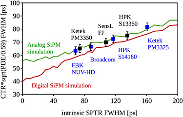
Figure 19. CTR shown as a function of the SPTR. CTR was measured with  LSO:Ce:0.4%Ca crystals wrapped in Teflon coupled with Meltmount and normalized, as if all the SiPMs would have a PDE of 59%. Monte Carlo simulations of the CTR were performed for an analog SiPM with high-frequency readout and a hypothetical digital SiPM combining all timestamps via maximum likelihood estimation. The simulations include 7 Cherenkov photons produced. Reproduction from Gundacker et al (2020).
Download figure:
Standard image High-resolution imageBy implementing optimized readout and pushing the electronics bandwidth, state-of-the-art SiPMs are even capable of delivering a CTR of 100 ps with 20 mm long crystals (Gundacker et al 2019), as shown in figure 20(a). Even more interesting, SiPMs, due to their excellent SPTR, are capable of utilizing the few Cherenkov photons produced in BGO leading to a CTR of 277ps FWHM for 20 mm long crystal (see figure 20(b)) and 158 ps FWHM for 3 mm long crystals (Gundacker et al 2019). Because the produced Cherenkov photons are so few, not all 511 keV events lead to the detection of prompt photons, hence, BGO shows additional long tails caused by the standard BGO scintillation. Whether these tails are acceptable for true TOF-PET reconstruction still has to be investigated, however, it should be mentioned that via proper readout strategies events can be identified and stated as being either in the peak or the tail, comparable to event identification in metamaterial approaches (Turtos et al 2019). Nevertheless much attention is given to BGO and many groups performed extended studies on it (Brunner and Schaart 2017, Kwon et al 2016, Cates and Levin 2019, Gundacker et al 2020, Kratochwil et al 2020).
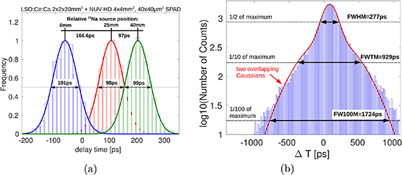
Figure 20. (a) With optimized SiPM readout using state-of-the-art devices it is possible to achieve a CTR of 100 ps FWHM with  LSO:Ce codoped with Ca crystals. (b) CTR obtained with
  BGO measured with HF-readout. Reprint from Gundacker et al (2020).
Download figure:
Standard image High-resolution imageWhen building a detector it is also important to know how the SiPM area and crystal size influences the CTR, for which a short summary is given in table 1. Basically it can be observed that there is some light loss, if the crystal cross-section approaches the SiPM area. This effect is more pronounced for short crystals and almost negligible for longer crystals. Increasing the SiPM area causes some deterioration in CTR due to the larger SiPM capacitance, but it is not tremendous, if high-frequency readout of the SiPM is being used.
Table 1. Best obtainable CTR with different SiPM areas (HPK  SPAD pitch) and LYSO:Ce crystal geometries in TOF-PET using high frequency electronic readout. Crystals were wrapped in Teflon and coupled with optical glue Meltmount (n = 1.58). Both SiPM types (S13360-3050PE and S13360-6050PE) have been operated at the same 10.5 V overvoltage and 16 °C temperature.
| 2 × 2 × 3 | 86 ± 2 | 91 ± 2 |
| 3 × 3 × 3 | 106 ± 1 | 101 ± 2 |
| 6 × 6 × 3 | 182 ± 2 | 117 ± 2 |
| 2 × 2 × 20 | 135 ± 2 | 134 ± 3 |
| 3 × 3 × 20 | 143 ± 1 | 136 ± 2 |
| 6 × 6 × 20 | 263 ± 2 | 159 ± 2 |


These examples should show the currently best achievable time resolutions and CTR limits with SiPMs in TOF-PET. Of course, building a PET detector with thousands of channels brings about various other problems. As there are integration and space limitations, limited power consumption, clock distribution only to name a few. Nevertheless, SiPMs have paved their way into TOF-PET due to the promise of excellent performances proven to deliver 100 ps CTR (in laboratory) and with the prospect of breaking this value even further towards 10 ps.
Prominent examples of commercial systems are the Vereos Digital TOF-PET/CT developed by Philips using digital SiPMs (Frach et al 2009) achieving a CTR of 300 ps FWHM, the Biograph Vision TOF-PET/CT from Siemens using analog SiPMs with refined readout architecture achieving a CTR of 210 ps FWHM (Conti and Bendriem 2019) and the launched whole body PET/CT from GE Healthcare named Discovery MI (Hsu et al 2017). The fact that all major players are using SiPMs in their high end TOF-PET/CT products can be seen as a confirmation of the overall superiority of SiPMs over PMTs, both in cost effectiveness and performance (Wagatsuma et al 2017).
5.4. SiPMs in PET/MR, SPECT/MR and Compton cameras
Hybrid scanners like SPECT/MR (single photon emission computed tomography combined with magnetic resonance imaging) and PET/MR were one of the main drivers of applying SiPMs in medical applications and paved the way for advanced TOF-PET systems discussed before (Bisogni et al 2019). The idea to combine PET with MR was evident after the success of PET/CT hybrid scanners in clinical applications. However, due to the magnetic fields present in MR-systems and the demand of having a simultaneous hybrid system, PMTs were not an option anymore (Zaidi and Del Guerra 2011). The first PET/MR systems were built using APDs as photodetectors, which could operate inside the MR. Interestingly, development on APDs was largely driven by HEP, as some calorimeters (e.g. CMS) operate in high magnetic fields and thus PMTs are not an option either (Deiters et al 2000). In the long run SiPMs comprised an attractive alternative to APDs, because of their much higher gain, faster rise time and much lower power supply voltage, which makes the integration in a system easier. After first attempts were made by several groups (e.g. Hong et al (2013)) the first commercial PET/MR system based on SiPMs was produced by GE Healthcare (Grant et al 2016). Preclinical PET/MR systems equiped with the Philips d-SiPM were studied around 2012 with impressive CTR results of 213 ps FWHM and a spatial resolution of 0.73 mm FWHM (Weissler et al 2012, Weissler et al 2015).
Hybrid systems combining SPECT with MR are rare, because SPECT has evolved to use different detectors like CdTe or CZT semiconductors for direct detection of the gamma rays (Bisogni et al 2019). For instance one project using RGB-HD SiPMs from Fondazione Bruno Kessler (FBK, Italy) and CsI scintillators is the INSERT project which developed an integrated SPECT/MR breast system (Busca et al 2015, Busca et al 2014, Occhipinti et al 2018).
SiPM based Compton cameras using scintillator crystals (e.g. LaBr3:Ce, CeBr3 or GAGG:Ce) recently gained a lot of attention due to their cost effectiveness and portability (Llosá 2019), especially in view of environmental radiation monitoring in homeland security connected with nuclear weapon assays, nuclear disasters, radioactive debris, etc. There are also applications in hadron therapy treatment monitoring, as they are expected to provide higher efficiency than collimated cameras for prompt gamma-ray detection (Llosá et al 2012, Llosá et al 2013). Nevertheless, in hadron therapy the radiation damage of the SiPMs still remains an issue. HEP is facing similar problems, which will be subject for discussion in the following chapters.
5.5. SiPMs in HEP
In the last 10 years SiPMs have become increasingly popular in High Energy experiments. The first large experiment that used 60k SiPMs was the neutrino detector T2K. They used one of the first fully commercial  , 50 µm pitch SiPMs from Hamamatsu (Vacheret et al 2011). The first Large Hadron Collider (LHC) experiment at CERN (European Organization for Nuclear Research) to use SiPMs was the Compact Muon Solenoid (CMS) general-purpose detector at the LHC. The CMS hadronic (HCAL) calorimeter is located in the large four Tesla CMS magnet and was originally readout by Hybrid Photo Diodes (HPDs) because of their magnetic field tolerance. In the last 5 years these HPDs were all replaced by > 18 k large area SiPMs leading to a better signal to noise ratio and long term stability as compared to the originally used HPDs. In order to satisfy the large linear range needed in the HCAL, i.e. one minimum ionizing particle (MIP) of about 2 GeV energy deposit to 500 GeV deposit for particle showers, CMS collaborated with multiple companies to develop 15 µm pitch SiPMs with > 4000 SPADs per square millimeter. The most challenging aspects of using SiPMs in a high energy experiment is an unusually high radiation environment and the gain and PDE dependence of the SiPMs versus temperature (breakdown voltage drift). Because the SiPMs are very compact the CMS-HCAL uses commercial peltier elements with a feedback loop in groups of 64 SiPMs packaged in 8 channel arrays to stabilize the temperature to 0.2 °C.
Radiation damage creates defects in the silicon, which increase the leakage current (Moll 1999) and can be expressed in an increased DCR in SiPMs (equation (17)) and the equivalent noise charge (ENC) can be calculated as in equation (18).


Here Id is the SiPM current, G the SiPM gain at a defined overvoltage, q the elementary charge (1.602 · 10−19C) and TI represents the integration time.
The dark count rate of most manufactures of SiPMs is below  . With radiation the DCR was expected to increase quickly with about
  for every
  (1 MeV equivalent) at an operating voltage of 3 V overvoltage at room temperature.
For example, figure 21 shows the average DCR increase for the 2.8 mm and 3.3 mm diameter SiPMs in the first year of operation in the CMS HCAL Endcap (HE). The total luminosity in CMS in the first year of operation with SiPMs was 67 fb−1 which gave  at 18 °C, equivalent to 2 p.e. noise for a 100 ns integration time of the plastic scintillator (Y11) pulses in the HCAL.
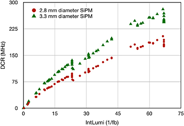
Figure 21. Average dark count rate increase as a function of luminosity of the HCAL SiPM at 18 °C and 3 V overvoltage.
Download figure:
Standard image High-resolution imageAt around 27 fb−1 and at the end of the year beam stop, annealing of the SiPMs was clearly visible. However annealing at room temperature was measured to be maximum a factor of 2–3. The total dose in the HE is expected to be  over the lifetime of the experiment for an expected integrated luminosity of 3000 fb−1. The maximum radiation dose for the SiPMs in the HCAL is in the barrel section (HB) with a total dose of
  . The expected DCR in the HB after 3000 fb−1 is 1.5 GHz and ENC of 12 p.e. at 3 V overvoltage at room temperature. To increase the S/N the peltiers can lower the temperate to 0 °C in order to lower the DCR by a factor of four and ENC by a factor of two.
5.1.1. CMS Endcap CE-H
After the successful operation of the SiPM in the HCAL there are two more projects in CMS that are considered for future upgrades that use SiPMs as their photodetector. The two projects are called the High Granularity Calorimeter (HGCAL) and Barrel Timing layer (BTL). The technical design reports of HGCAL are referenced in CMS, (2017). The HGCAL is mainly readout by 600 m2 silicon sensors in the high radiation areas. In the lower radiation area with a fluence of  it is possible to design a cheaper solution of plastic scintillating tiles with SiPM readout (Chang 2019).
In contrast to the existing HCAL HE, where the SiPMs are separated from the scintillators and readout by optical fiber connection between the scintillator and SiPMs, in this design the SiPMs are directly installed on small  scintillating tiles. This so called SiPM-on-tile design was first introduced by the CALICE collaboration. The scintillator is formed into small tiles and scintillation light is directly readout by an SiPM that is optically coupled through a small 'dimple' in the centre of one face of each tile. The SiPMs are mounted on a printed circuit board which is then mated with the appropriate tiles. This system is illustrated in figure 22.

Figure 22. Example of three CALICE  scintillator tiles mounted on a PCB that holds one SiPM per tile. The left two scintillators are unwrapped to show the SiPM within the small dome at the centre of the tile, while right-most tile is wrapped with reflective foil.
Download figure:
Standard image High-resolution imageThis geometry makes it possible to have a much finer segmentation to complement the fine segmentation and high granularity of the silicon sensors. The total amount of tiles with SiPMs needed for this project is 250 k for both End-Caps. The disadvantage of this SiPM on tile design is that the SiPM will see a much higher up to 8 · 1013 1 MeV equivalent neutron fluence. This is made possible by cooling the entire End-Caps to −30 °C.
5.1.2. BTL Timing layer
The Barrel Timing layer (BTL) is planned to be situated inside the Tracker support tube in CMS. Its main function is to measure the timing of minimum ionizing particle (MIP) signals with a precision of 30–50 ps (sigma single). The basic element of the BTL is a 16 channel array of  LYSO:Ce crystals readout on each side by a 16 channel array of
  SiPMs (see figure 23) For the full installation the total number of 16 channel SiPM arrays is almost 30 000.
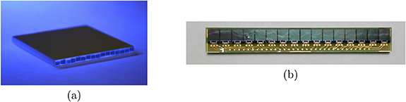
Figure 23. (a) BTL 16 channel LYSO:Ce array. (b) BTL 16 channel SiPM array.
Download figure:
Standard image High-resolution imageOne of the major challenges is the radiation damage induced high dark count rate, which especially for timing is an issue. Interestingly the challenges are very close to applications with high background (ambient) light, as in the case of LIDAR. Especially for the case of the BTL timing layer the dependencies of the time resolution of dark counts have been studied in more detail and are presented below.
The timing resolution of a detector like BTL has many jitter contributions and can be summarized, as in equation (19). With  the clock distribution jitter,
  the digitization induced jitter,
  the electronic contribution,
  the photostatistic contribution of the scintillation emission and
  the dark count rate induced noise equivalent timming jitter.

The timing performance drivers from the SiPM point of view are the photo-statistics (PDE and SPTR) and the noise term due to DCR (especially in the case of high DCR values). Thus major R&D efforts have been made towards the optimization of the SiPMs. The contribution from photostatistics at zero DCR is related to the stochastic fluctuations in the time-of-arrival of photons detected at the SiPM and is well known to be inversely correlated to the square root of the number of photoelectrons ( ), i.e.
  .
.
A bench measurement (CMS 2019) of the timing dependence of the  and DCR is shown in figure 24(a) using an LED with a pulse time spread of 350 ps rms. Due to the large expected radiation fluence of
  in the BTL the DCR is expected to rise to 40 GHz even at an operating temperature inside the tracker tube of −30 °C. The DCR noise term will quickly be the dominant factor in the timing resolution. For the DCR measurement in figure 24(b) the LED intensity was first set to a value of about 390 photoelectrons yielding a time resolution, in absence of DCR, of about 15 ps sigma which is just above other jitter sources in the experimental setup.
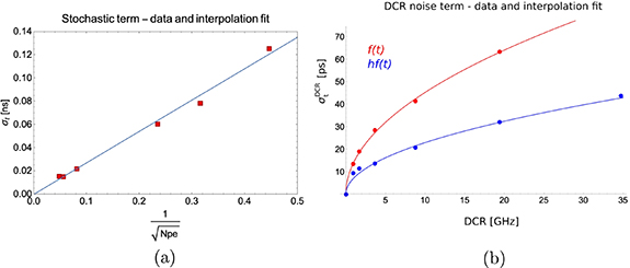
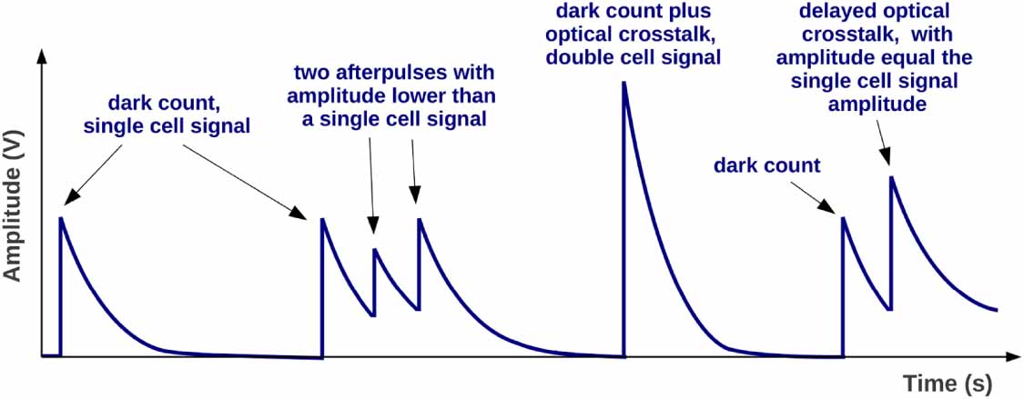
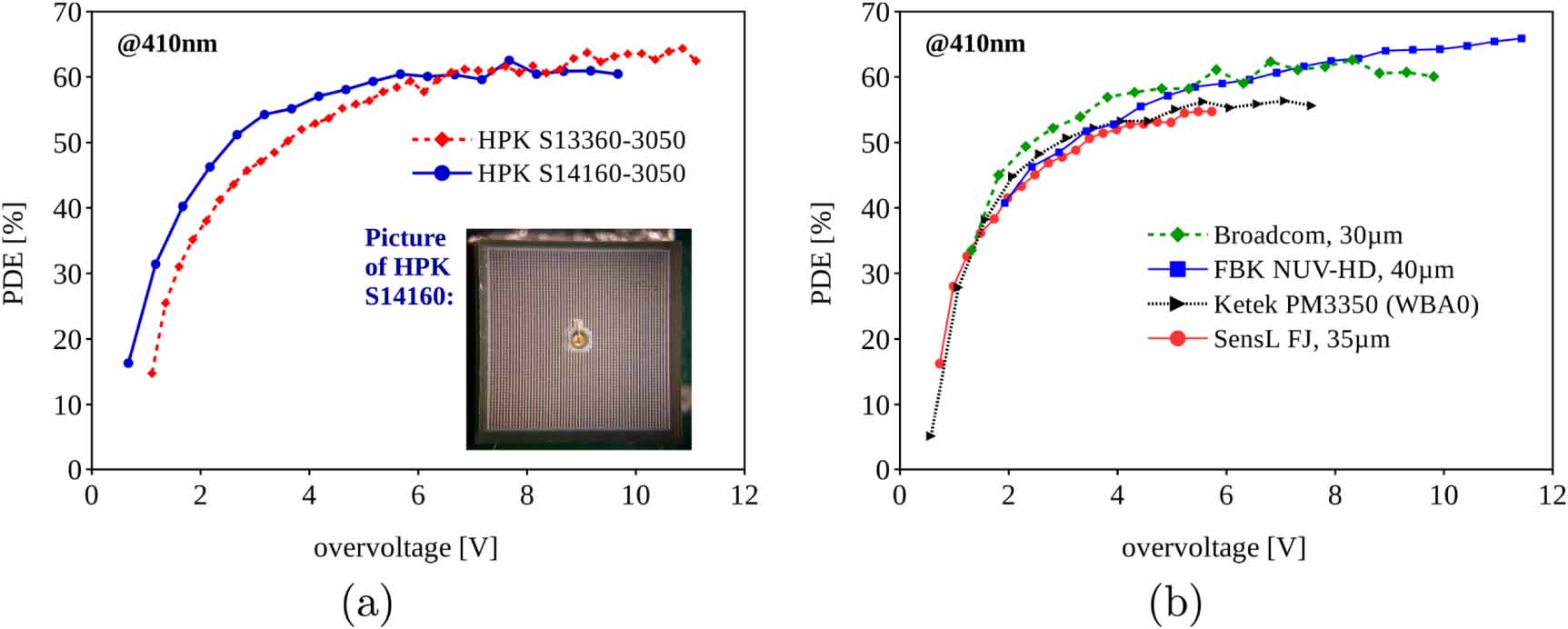
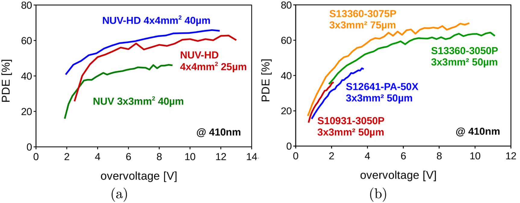
Figure 24. (a) Time resolution of the SiPM for different signal amplitudes for DCR = 0 GHz. (b) Additional time jitter due to DCR up to 35 GHz measured by injecting randomly distributed light on a BTL SiPM for a signal of 390 photoelectrons.
Download figure:
Standard image High-resolution image
The benefit of using a constant fraction algorithm hf(t) as compared to a simpler leading edge approach f(t) is shown to be important when the DCR increases (as can be seen in figure 24(b)). In order to obtain hf(t), the signal f(t) is processed such that the waveform is inverted and delayed and then summed up with the original pulse resulting in a pulse defined by  . In this way the resulting waveform has smaller baseline fluctuations from the DCR. Measuring the constant fraction timing resolution as a function of the
  for the highest 40 GHz DCR a
  relation can be found.
To summarize, the contribution of the dark count rate (DCR) to the time resolution can be expressed as in equation (20).
Here it can be seen that the DCR has the same influence as electronic noise to the time resolution with the noise amplitude proportional to the square root of the DCR. Further, the time resolution can be improved drastically by increasing the signal to noise ratio, i.e. the detected light intensity.
6. Discussion and outlook
The progress made in analog SiPMs over the last decade has been extensive, improving on all aspects, e.g. PDE, SPTR, afterpulse, crosstalk, etc. This, however, has set severe challenges on the front-end readout electronics, because the SiPM characteristics (signal shape and multiplication gain) have changed at an even pace bringing new devices almost every year. Today, the high maturity of analog SiPMs provides for more long-lived devices on the market, which allows for the optimization of the electronic readout systems. Additionally, newer devices while improving on aspects like PDE at different wavelenghts, SPTR, etc tend to operate at similar overvoltages and have similar device capacitances. This makes the SiPM integration and modernization in systems easier to plan with a clear benefit for industrial products in the medical sector, automotive, biological applications and so forth.
Nevertheless, in medical imaging in particular the challenges of using SiPMs instead of PMTs lie in the high number of readout channels (several tens to thousands). Application-specific integrated circuits (ASICs) are able to cope with that number of channels, in part due to advancements regarding integrated design processes in deep-submicron technology, with 28 nm or 14 nm feature size. However, the drawback of using such highly integrated ASICs is the high cost and the need of design specialists. Another challenge is the assembly of the detector-system with proper routing of all signal lines. An early digitization, best directly on the SiPM, might be a viable solution to this problem. And indeed various research groups are working on this with analog SiPMs (Muntean et al 2018), digital SiPMs (Frach et al 2009) or fully 3D assembly of digital SiPMs (Bérubé et al 2012). Indermediate concepts on the way to the fully digital SiPM could be to amplify each SPAD signal with its own amplifier and combine the signals afterwards with an analog sum, or with an fast OR-gate (Nolet et al 2016).
The fully digital SiPM able of addressing each fired SPAD can in addition resolve the position of each impinging photon. This is important in Lidar cameras or the discrimination of small scintillator pixels in a crystal-matrix coupled to the SiPM in preclinical high-resolution small animal PET. New developments like position sensitive analog SiPMs are able to reduce the number of readout channels drastically with excellent spatial resolution of impinging photons on the SiPM. Examples of this technology are the linearly graded position-sensitive SiPM developed by FBK (Gola et al 2013, Ferri et al 2015, Du et al 2015), and the sensitivity encoded or interpolating SiPM (Schulz et al 2013, Fischer and Piemonte 2013).
Newest developments of SiPMs lead to extented PDE in the VUV (Gola et al 2019), which was shown to open new doors in the study of cross-luminescence crystals (Laval et al 1983) for fastest timing applications (Gundacker et al 2020). On the other side of the spectral range it was demonstrated that proper electric field design in the SPAD significantly improves the PDE in the red to infrared for LIDAR applications (Acerbi et al 2018c). Such electric field optimizations have a direct impact of boosting the SPTR and PDE of SiPMs.
With the SiPM having improved on so many levels, e.g. the PDE already reaches values of up to 70% at 410 nm, the SPTR is one remaining key parameter for further progress. For example, highest SPTR with values anticipated down to 10 ps is needed for ultimate timing in Cherenkov PET, which will only be possible with parallel efforts on electronic readout (Gundacker et al 2020, Cates et al 2018, Cates and Levin 2019).
Last but not least SiPMs due to their compactness, low power-consumption and continued integration of the readout electronics with further miniaturization will allow the realization of medical devices not possible with e.g. PMTs. As an example SiPMs were employed in the EndoTOFPET-US project, with the aim to built an endoscopic probe for pancreatic and prostate cancer, equiped with a PET head (Frisch 2013). In this special case, because of the missing ring geometry TOF becomes a very important aspect, where SiPMs can play to their strengths. Such novel systems could be used not only to improve diagnostic data but to guide surgical interventions as well (Bisogni et al 2019).
7. Conclusion
This paper introduced the basic working principles of SiPMs and discussed their most important defining parameters, e.g. dark count rate, crosstalk, afterpulsing, breakdown voltage, electrical model, etc. A highlight and closer explanation of applications where SiPMs are currently gaining more and more importance was given, e.g. in TOF-PET and HEP. The main spotlight was on the analog SiPM, merely because of its high maturity with excellent devices available on the market and intense research activities ongoing.
The analog SiPM is expected to see major improvements in single photon time resolution, which is currently a subject for in-depth research. Present-day PDE is already reaching values of up to 70% in devices with large single photon avalanche cells, and only little improvement in these devices can be expected. Nevertheless, in order to reduce correlated noise and increase the dynamic range of the SiPM, research is moving in the direction of smaller cell sizes. Hence, the PDE is still a subject for research and improvement, since in devices with small cell sizes, the effective fill factor plays a crucial role.
In this sense, the prospect of the analog SiPM might go in the direction of high dynamic range devices, with low crosstalk and afterpulsing together with excellent single photon and time resolution. Further research is continuing in devices applicable for LIDAR with improved detection sensitivity for photons in the red to infrared. On the other spectral range devices are being improved for the detection of UV light for dark matter search, applicable to the detection of cross-luminescence in scintillators. Besides the ongoing improvement of standard Silicon devices other materials are subject to research, like gallium arsenide (GaAs), indium gallium arsenide (InGaAs) or silicon carbide (SiC).
The digital SiPM might however ultimately be the device of the future, due to its promise of being the perfect photodetector by processing each single photon independently. Of course, research done on the analog SiPM is directly applicable to the digital SiPM, if 3D integration is applied. Just to mention one example, the digital SiPM would make it possible to build a single photon sensitive time imaging camera (allowing for lens-less LIDAR cameras).
Single photon detection with excellent time resolution is important for innumerable applications, truly rendering the story of SiPMs to be continued for a very long time.
Acknowledgments
This work has received support from the Crystal Clear Collaboration (CCC) and special thanks goes to Etiennette Auffray and Paul Lecoq. The authors further want to thank Tina Vernon for thoroughly proofreading this manuscript. Last but not least we want to thank all physicists, engineers and technicians who we had the pleasure to discuss and work with the past years. Without that multitude of our really great colleagues this manuscript would not have been possible.