
Abstract
In this work we demonstrate a two-pixel solid-state photoluminescent device able to emit white light covering the entire visible spectrum from 380 nm up to 800 nm. The device is based on a combination of porous Si, hydrothermally grown ZnO and carbon quantum dots, in a two-pixel formation, with porous Si and ZnO acting independently while the carbon quantum dots are deposited on top of the entire device. All processing is done using standard Si processing techniques. Moreover, the device design allows for tunability of the emitted spectrum simply by choosing the desired combination of the materials. Overall, the demonstrated device is low cost, environmentally safe and biocompatible.
Export citation and abstract BibTeX RIS

Original content from this work may be used under the terms of the Creative Commons Attribution 4.0 licence. Any further distribution of this work must maintain attribution to the author(s) and the title of the work, journal citation and DOI.
1. Introduction
White light emission has become a very important effect due to its application in displays, light emitting devices [1] and sensors [2–4]. More specifically, a host of different materials have been used to accomplish this effect, including yellow phosphor materials in combination with Si or III–V semiconducting diodes [1], organics [5], perovskites [6], quantum dots[7], metal-organic frameworks [8, 9] and others. In terms of device architectures, a variety of combinations ranging from the use of three different color pixels [1] down to single emissive layers [10, 11] are being researched.
Of special interest are materials and device architectures that can be processed in solid-state and are compatible with standard Si processing techniques. These materials offer the possibility of full integration with Si-based electronics for compact and highly efficient devices, especially in the case of sensors. So, for example, even though significant effort has been made on creating stable white light emission from perovskites [12–15], these materials are yet far from being CMOS compatible. In addition to good performance, any device must be low-cost and environmentally friendly. Moreover, for applications where bio-detection is demanded, bio-compatibility is also a requirement. So, well-researched, non-toxic, and bio-compatible materials which can be processed by standard batch Si fabrication techniques are excellent candidates.
Towards that direction, porous Si and ZnO are two potential candidates. Their luminescent properties have been very well researched and their compatibility with Si processing well documented. Porous Si primarily emits in the red/yellow wavelengths [16, 17], while ZnO in the green/blue ones [18]. For these reasons, the combination of the two materials has sparked significant interest in terms of creating tunable photoluminescent materials. The most common approach is the creation of a composite material through the deposition of ZnO on a porous Si substrate and a subsequent annealing process [18–29]. This approach follows the single emissive layer route for white light creation. Some success with creating white light has been demonstrated using this approach, even though not for the entire visible spectrum (380–750 nm). For example, composite porous Si/ZnO materials have been shown to emit on wavelengths between 380 and 680 nm [24] or from 550 to 850 nm [30]. Very little effort has been made to combine the two materials in a device structure that independently utilizes their properties [28].
In this work, a novel approach for combining these two materials to create white light photoluminescence (PL) is presented. A device structure with two distinct areas, namely porous Si and hydrothermally grown ZnO is fabricated. The two areas are simultaneously exited by the same laser pulse and the overall emission of the device is shown to be the combination of each component's emission. The definition of the independent areas is performed using standard Si processing techniques. The device emission is shown to cover most of the visible spectrum except emission corresponding to blue. To cover that part of the spectrum without creating a composite material, carbon quantum dots are used. The addition of the quantum dots is shown to complete the emission, creating a device that emits white light covering the entire visible spectrum. The presented approach utilizes only well researched materials and industrial methods, has a very simple design and is, by nature, cost-effective, environmentally safe and bio-compatible. Moreover, it allows for tunability of the emitted spectrum as the three materials used can be combined in several independent ways. It also allows the opportunity for different device architectures for additional tunability without the difficulties of creating repeatable and stable composite materials through high temperature annealing steps.
2. Experimental
2.1. Porous Si
Porous Si was formed by electrochemical etching of Si, a process known as anodization [16, 17]. A p-type Si substrate (6–8 Ω cm) is used as the anode in an electrochemical cell with a Pt mesh acting as the cathode. An electrolyte of 60% ethanol and 40% HF (50% in H2O) is used with a constant current density of 80 mA cm−2. This is a typical process for developing porous Si in a sponge-like form with a porosity of 63% and pore sizes in the few nanometer range [31, 32]. Under the described conditions, the thickness of the porous Si layer depends solely on the duration of the anodization process. For the following experiments a thickness of 10 μm was chosen for all samples. A scanning electron microscope (SEM) cross-sectional image of a typical porous Si layer on Si is presented in figure 1. Oxidation of porous Si samples was also performed at temperatures of 700 °C and 800 °C.

Figure 1. Porous Si layer (10 μm thick) on a Si substrate.
Download figure:
Standard image High-resolution image2.2. ZnO
ZnO thin-films were synthesized using the hydrothermal method on seeded substrates [33–35]. In short, the two-step process starts with the creation of a sol–gel solution by dissolving zinc acetate dihydrate in absolute ethanol with a concentration of 40 mM, by mixing at 60 °C for 1 h. The resulted sol–gel is aged in a sealed container for 24 h. The aged solution is then spin-coated on the samples (Si and porous Si) at 1000 rpm for 30 s. A baking step at 500 °C for 10 min on a hot-plate in air follows. This process is repeated 10 times resulting in a complete seeding layer. In the second step, the films are hydrothermally grown in an aqueous equimolar solution of zinc nitrate hexahydrate and hexamethylenetetramine with a concentration of 200 mM, at 87 °C for 2 h. The resulted thin-films are semi-continuous with a thickness of 1 μm. Representative top–down and cross-sectional SEM images of a ZnO film grown on a Si substrate are presented in figures 2(a) and (b), respectively. The seed layer can be clearly distinguished from the hydrothermally grown film and its thickness is measured to be close to 30 nm.

Figure 2. (a) Top–down and (b) cross-sectional SEM images of the grown ZnO layer on Si.
Download figure:
Standard image High-resolution imageIn order to locally grow ZnO layers on porous Si substrates a process was developed and is described schematically in figure 3. At first, porous Si is formed on a Si substrate. The seed layer is then span-on. A photolithography step is then used to cover the desired areas with photoresist. The hydrothermal growth of the ZnO follows, which produces a ZnO layer only on the areas not covered by the photoresist. Finally, the photoresist is removed by acetone leaving a sample with the 1 μm thick ZnO layer only on the desired areas.
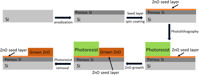
Figure 3. Schematic representation of the process developed in order to produce locally defined ZnO layers on porous Si substrates.
Download figure:
Standard image High-resolution imageTo demonstrate the feasibility of white light creation through the use of locally defined ZnO layers on porous Si, a simple structure was selected. The structure consists of simply defining half the sample area to have ZnO. Top–down and cross-sectional SEM images of the edges of the created structures are presented in figure 4. The images in figure 4 demonstrate the success of our developed process. The almost 45° angle of the ZnO layer edge is due to the morphology of the photoresist after the photolithography step. It is also worth noting that the ZnO seed layer has the same thickness on the porous Si substrate in both areas with and without the grown ZnO layer, implying that the ZnO does not enter the porous Si structure, something expected from its very small pore size. This fact allows the stack of materials presented to be treated as independent and not as a composite material.
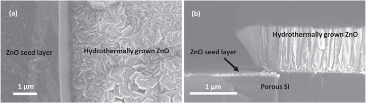
Figure 4. (a) Top–down and (b) cross-sectional SEM images of the lithographically defined ZnO layer on porous Si.
Download figure:
Standard image High-resolution image2.3. Carbon quantum dots
The carbon quantum dots were prepared by adding 3 g of citric acid and 3 g of urea in 10 ml of H2O under magnetic stirring. The solution was then heated in a microwave oven operating at 800 W for 4 min The product of this reaction was placed in an oven at 60 °C for 1 h to remove any potentially remaining volatile byproducts, before being re-dissolved in H2O and centrifuged at 3000 rpm for 20 min The supernatant was then collected and dried in an oven at 60 °C overnight to create a powder. A 20 mg ml−1 aqueous solution was then prepared and drop casted on the substrates. The substrates were then placed on a hot plate at 80 °C for the H2O to dry. More details on the preparation of the carbon quantum dots as well as their characterization can be found in [36, 37].
2.4. PL characterization
For the PL characterization of the samples a pulsed nitrogen laser of Thermo Laser Science was used as the excitation source, lasing at 337 nm with pulse energy of 150 μJ and repetition rate of 20 Hz. The laser beam was passed through a 337 nm band pass filter. The laser spot was a rectangular, 7 mm length by 2 mm width. The PL spectrum was selected by a suitable lens coupled to an optical fiber to the spectrophotometer LR1 of ASEQ-Instruments monitored by a PC.
3. Results and discussion
The measured PL intensity of as-fabricated and oxidized at 700 °C and 800 °C porous Si layers as a function of wavelength is presented in figure 5(a), along with Gaussian fits to help identify the peak wavelengths. The as-fabricated layers exhibit a very small peak around 659 nm. The oxidation process leads to a significant increase in intensity and a red shift while increasing the oxidation temperature leads to a blue shift for the intensity peak. These results are commonly observed in PL measurements of porous Si layers. A possible explanation for these two observations can be given through a combination of surface state passivation combined with a reduction of the nano-crystallite size due to the oxidation process [16, 17, 38]. Oxidation at lower temperatures is effective at passivating surface states thus increasing the observed PL signal, slightly shifting it towards longer wavelengths, while larger temperatures lead to a reduction in nano-crystalline size, causing a blue shift of the signal. For the rest of the presented work, porous Si oxidized at 700 °C was selected because of its increased intensity, but also because its peak is slightly shifted towards the red color compared to the other conditions. We have made this choice in order to include the widest possible range of visible wavelengths in our final structures. From this point forward we will refer to samples oxidized at 700 °C for 30 min simply as 'porous Si'. It is noted that the addition of the ZnO seed layer on top of the porous Si layer does not produce any measurable change to the PL spectra, as can be seen in figure 5(a), presumably due to its very small thickness (about 30 nm).

Figure 5. Photoluminescence intensity as a function of wavelength for (a) porous Si (as-fabricated, oxidized at 700 °C and 800 °C and oxidized at 700 °C with a ZnO seed layer), (b) ZnO on porous Si, (c) carbon quantum dots on Si and (d) carbon quantum dots on porous Si. Gaussian fits that represent the measured peaks are also presented for (a)–(c). In the case of (b) and (c) where multiple peaks are present the cumulative fit is also presented.
Download figure:
Standard image High-resolution imageThe PL intensity of the ZnO layer grown on a porous Si substrate is presented in figure 5(b). It is evident that two distinct peaks are present which can be fitted with two Gaussian curves with peaks at 383 nm and 572 nm, respectively. This is the anticipated PL behavior of ZnO, with the UV peak attributed to exciton recombination and the visible, secondary, peak attributed to transition from oxygen vacancy energy levels within the band gap to the valence band [18, 19, 28]. In fact, the PL spectra of our ZnO layers are identical for both Si and porous Si substrates. This is the motivation for using such a 'thick' ZnO layer, to mask any contribution from the porous Si substrate making the responses of the two materials independent.
The PL intensity of the carbon quantum dots on Si are presented in figure 5(c). The spectrum is composed of two peaks at 406 and 521 nm, consistent with previous studies on these dots in the solid state [37]. The spectrum is presented on a Si substrate in order to isolate the behavior of the carbon dots. When deposited on a porous Si substrate, the spectrum unavoidably includes the emission of the porous Si as well, as demonstrated in figure 5(d).
The PL spectra presented in figure 5 lead to several interesting conclusions. The first is that the materials created, namely porous Si, ZnO and carbon quantum dots, all behave in the manner expected by the literature. The second is that the grown ZnO layer is thick enough to block any porous Si emissions from underneath it, while the ZnO seed layer is thin enough to not influence PL emissions. Moreover, the effect of the carbon quantum dots on the spectra is purely additive, meaning that the addition of the dots on the porous Si, for example, produces a spectrum that is the addition of the quantum dots spectrum and the porous Si spectrum. The materials act independently in terms of PL spectra. More importantly, the addition of all the presented spectra covers the entire visible spectrum. In order to demonstrate that, the structures described schematically in figure 3 were created. Excitation of these structures with the 337 nm laser was performed in a manner that 50% of the laser spot was on the ZnO structure while 50% was on the porous Si. The detector measured the sum of the emissions. A schematic representation of the described structure along with an optical picture of the created emission is presented in figure 6. The PL emission spectrum of the developed structure is also presented in figure 6. As expected, the emission from the grown ZnO layer appears as yellow while the one from the porous Si as red in the optical picture. The PL spectrum detected by the detector is simply the addition of the two material spectra.
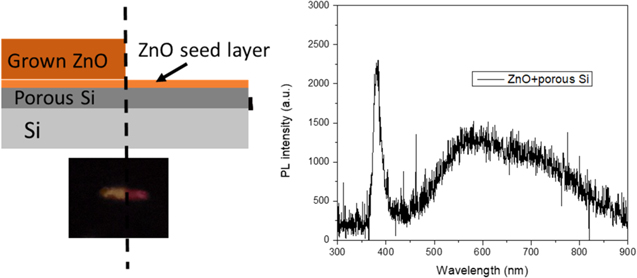
Figure 6. Schematic representation of a ZnO/porous Si structure. An optical image of the PL emission is presented underneath the schematic. On the right-hand side of the schematic the measured PL spectrum is presented.
Download figure:
Standard image High-resolution imageCarbon quantum dots were deposited on the 2-pixel structure described in figure 6 to add their PL spectrum, as well. A schematic representation of the new structure with the dots is presented in figure 7. As before, an optical picture of the emissions of the laser spot are presented underneath the schematic and the detected PL spectrum of the entire structure is presented on its right-hand side. Gaussian fits for each individual emission peak are also presented, along with their cumulative fit. The addition of the dots did not significantly affect the emission color of the ZnO part. It has been previously demonstrated that the presence of ZnO quenches the emission of the carbon quantum dots due to electron-hole recombination caused by non-radiative electron transfer between the materials [39–41]. On the other hand it turned the porous Si part from red to purple, as expected. Moreover, the PL spectrum of the created structure covers the entire visible spectrum starting from the UV (382 nm) all the way up to at least 800 nm, creating, in effect, white light. To the best of our knowledge, this is the first demonstration of such a wide coverage of the visible spectrum by PL emission from this set of materials.

Figure 7. Schematic representation of a ZnO/porous Si/carbon quantum dots structure. An optical image of the PL emission is presented underneath the schematic. On the right-hand side of the schematic the measured PL spectrum is presented along with Gaussian fits of the relevant peaks.
Download figure:
Standard image High-resolution image
Also, the analysis of the PL spectrum using the Gaussian fits reveals that the structure emits the sum of the individual materials emissions, as designed. This fact allows for a versatile and controllable design of the PL emissions from these low-cost, environmentally friendly, biocompatible, and stable solid-state materials. The presented method offers the potential of developing pixels of different sizes, shapes, and area coverage, creating any color combination, including white in a very controllable fashion. The method developed in this work, relies solely on the creation of distinct pixels using micro-fabrication methods and known materials and does not depend on the creation of composite materials.
4. Conclusions
In conclusion, a solid-state photoluminescent device based on porous Si, hydrothermally grown ZnO and carbon quantum dots has been demonstrated. The device is based on creating a two-pixel structure, namely porous Si and ZnO using standard Si processing. Carbon quantum dots are deposited on top of the entire device. The recorded PL spectrum is shown to be the combination of its individual components with no composite material phenomena present. Each component is shown to have the expected PL behavior from the literature, namely porous Si emitting at 700 nm, ZnO emitting at approximately 380 and 570 nm and carbon quantum dots emitting at approximately 500 and 520 nm. Different combinations of these materials are shown to produce the combinations of their individual PL spectra, demonstrating the tunability of the PL emissions. The 2-pixel structure with the addition of the carbon dots is shown to produce a PL spectrum that covers the entire visible spectrum from 380 nm up to 800 nm, thus demonstrating white light emission.
Data availability statement
All data that support the findings of this study are included within the article (and any supplementary files).