

Abstract
We present a simple, but rapid and accurate approach to identify the layer number of graphene oxide (GO) by using its thermally enhanced optical contrast via vacuum heating. As expected, changes have been observed both in the thicknesses and chemical structures of the material upon the thermal treatment, which can be attributed to the reduction of the amount of intercalated water and oxygen content. This results in the increase of refractive index and absorption coefficient approaching the values for intrinsic graphene. Finally, we achieve an almost complete recovery of optical contrast of GO compared with the one of graphene. The method would be made suitable for the thickness identification of mass-produced GO since it can greatly facilitate sample evaluation and manipulation, and provide immediate feedback to improve synthesis and processing strategies.
Export citation and abstract BibTeX RIS
1. Introduction
The critical ingredient for the discovery of graphene in 2004 was the observation that graphene becomes visible under a normal optical microscope when exfoliated on substrates consisting of a silicon wafer with a 300 nm thick silicon dioxide layer [1]. Subsequently, graphene has been extensively studied and inherited a series of unique physical and chemical properties, which predicts its huge potential applications in different sectors ranging from chemical sensors [2] to energy [3], flexible display [4], optical tweezers [5, 6] and photodetectors [7]. There are two origins of the visualization of graphene on this specific substrate. Firstly, graphene itself has a universal optical absorption in visible range (∼2.3% for a single layer with refractive index of 2.0-1.1i and thickness of 0.335 nm) [8]. Secondly, the interference effect from the SiO2/Si multilayer structure would enhance the absorption of light [9, 10]. Graphene oxide (GO) is the most promising precursor for solution processed, chemically modified graphene for applications such as photovoltaic cells [11, 12], capacitors [13, 14], sensors [15, 16], and transparent electrodes [17, 18]. However, due to the use of strong oxidizing agents to yield GO, a sizeable optical gap caused by sp3 hybridization of oxygen groups is opened up and a large amount of intercalated water is introduced between the GO layers. As a result, the optical absorption of GO becomes weaker than graphene. This means the optical visibility of GO is almost only caused by extra interference path from SiO2/Si substrate, it is thereby more challenging to visualize single- and few-layer GO under optical microscope. Currently, atomic force microscopy (AFM) is the most direct way to visualize GO and give accurate thickness values [19], but it is a completely impractical method for quick sample examination over large areas. Scanning electron microscopy (SEM) and fluorescence quenching microscopy can be much faster [19–21], but still not capable to identify the number of GO layers. Imaging ellipsometry is a powerful technique for identifying GO sheets in terms of thickness [10], however, the strict requirements of illuminating wavelength may limit its general adaptation. White light contrast spectroscopy also has been employed to evaluate the thickness of GO (up to 8 layers), but it is found that the contrast value for single-layer GO is only 0.035, and the average increment for adjacent GO layers is ∼0.025 [22], which is not accessible to distinguish the difference obviously and unambiguously. In addition, it should be noted that the value could be even lower if the as-synthesized GO sample possesses higher oxidation degree.
As explained previously, chemically derived GO is an attractive material for various industrial applications (commercial scalability), so it is quite demanding to establish how synthesis and processing conditions would affect the final sample quality, such as the lateral and vertical dimensions distribution of the sheets, especial for the latter (i.e. thickness). However, the above tools for charactering the GO material are not tailored for quick and large-scale samples examination due to low throughput. Therefore, a simple and more efficient approach that allows quick and accurate thickness identification of GO is highly desirable. In this work, we successfully identify the number of layers of GO by utilizing vacuum thermal treatment to enhance its optical contrast. With the stepwise increase of annealing temperature, we observe a corresponding stepwise increase of optical contrast of GO, and finally obtain an almost complete recovering of the contrast value at high annealing temperatures as compared with that of intrinsic graphene. A qualitative explanation for the recovery of contrast has been discussed, based on the removal of intercalated water and oxygen groups in GO layers upon the thermal treatment. This results in a significant increase in the effective values of refractive index and absorption coefficient of the material, respectively. This method has the advantage of being quick and accurate, and capable for large-scale investigation, which is very suitable for the thickness identification of industrial GO samples.
2. Experiment
GO was synthesized using a modified Hummers method, detailed preparation process can be obtained from reference [23]. The individual GO sheets were obtained by spin-coating the GO aqueous suspension (at 1000 rpm for ∼1 min, <2 mg ml−1) on 285 nm SiO2/Si substrate for optical microscopic investigation. The GO thin film was achieved by dropping the GO aqueous suspension (5–10 mg ml−1) on quartz substrate, and then keeping for ∼10 min, finally spin-coating at 650 rpm for ∼1 min. After spin-coating, all as-deposited GO samples were dried in ambient conditions and then stored in a vacuum container. To obtain a defined number of layers of as-deposited GO sheets, the sheets were firstly located on the substrate by using optical microscope Olympus BX41M-LED with different magnification of objective lens (10×, 20× and 50×). After that, AFM scan (asylum research MFP-3D) was performed within the same area to trace the targeted sheets and then identify their thicknesses. Optical images for contrast investigations were taken under a 50× objective (NA = 0.5). Morphology of the GO thin film was acquired by SEM with a FEI Inspect F50 system. UV–vis absorption spectroscopy was carried out to analyze the optical absorbance of GO thin film. Raman spectroscopy was carried out using a JY HR800 micro-Raman system with excitation wavelength of 514.5 nm. The thermal reduction of GO was performed in a tube furnace (OTF-1200X) with various annealing temperatures in the range of room temperature (RT) to 950 °C in vacuum (∼0.1 Pa) for 30 min.
A total of four monolayer GO samples deposited on 285 nm SiO2/Si substrate were annealed at temperatures of 180 °C, 350 °C, 650 °C and 950 °C, respectively. The heavily doped p-type Si wafer was used as a common back-gate electrode for reduced GO devices, and the 285 nm SiO2 layer was used as the dielectric layer. Source and drain electrodes (5 nm Ni adhesion layer, followed by a 50 nm Au capping layer) were defined using electron beam lithography and then deposited by thermal evaporation. Electrical transport characteristics of these devices were measured in ambient conditions using a Keithley 2612 semiconductor analyzer.
3. Results and discussion
Due to the weak optical absorption that originates from both the large optical gap caused by sp3 hybridization of the oxygen groups and the intercalated water in GO layers, pristine GO is almost transparent in visible regions, and therefore exhibits a feeble visibility under optical microscopic investigation, as shown in figure 1(a). We subsequently perform a stepwise reduction of the GO sample by means of vacuum thermal annealing from 90 °C to 800 °C. Figures 1(b)–(f) show the corresponding optical images of GO on 285 nm SiO2/Si substrate following different temperature annealing, respectively. The sample shows four areas of different optical contrast, which are due to the local two/three/four folding of single-layer flakes. With the increase of annealing temperatures, it is found that GO sheets can be readily visualized with good optical contrast, and the edges and overlaps are also observed clearly. Meanwhile, it shows that the increase of visibility of GO sheets during the entire thermal annealing process is significant, especially for the temperature range from RT to 180 °C. Accordingly, we quantitatively measure the contrast values of GO sheets with different annealing temperatures. The contrast values at each pixel can be calculated from image using the equation below [9, 24]:
where Rsub(G) and RGO(G) are the respective green (G) channel values taken from the optical images of the substrate and GO sample by Matlab software. During the experiment, we find that the light illumination under a microscope is non-uniform, which will make it inaccurate to evaluate the thickness of GO by taking a fixed contrast value of Rsub(G) from the optical contrast image. To end this, the light illumination correction has been considered during the image processing procedure, that is, an optical image of a clean substrate was taken under the same illumination and used as background for obtaining Rsub(G) at each pixel.
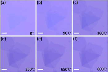
Figure 1. (a)–(f) Optical images of GO sheets taken after different temperature annealing from RT to 800 °C, scale bar = 5 μm.
Download figure:
Standard image High-resolution imageThe results after light illumination correction are shown in figure 2. We plot the evolution of optical contrast as a function of annealing temperature in figure 2(a), and the values are taken from four different areas of the GO sample. A corresponding increase of the contrast values by raising the temperature gradually is clearly observed. This trend is in line with the observation of these images shown in figure 1, especially of the GO contrast values which significantly increase even after mild annealing in low vacuum (30 min, 180 °C, ∼0.1 Pa), the increase for the few-layer GO following thermal treatment is greater than the increase found in the case of the single-layer GO. More intriguingly, as shown in figure 2(b) the contrast values of annealed GO with different thicknesses at high annealing temperatures (e.g. for 800 °C annealed GO, red points) can be compared with those of mechanically exfoliated graphene (blue points). The value for single-layer GO is about 0.077 ± 0.008, and it increases linearly with the sample thickness, for example, 0.130 ± 0.012, 0.174 ± 0.007, and 0.214 ± 0.012 for two, three, and four layers, respectively. It should be mentioned that even if GO samples are centrifuged, dried in air and redispersed in other polar solvents such as ethyl alcohol, they still show similar effects on contrast enhancement. One to four layers of graphene are also fabricated on the same batch SiO2/Si substrate and the corresponding contrast values are obtained under the same conditions. Additionally, for reference, a stepwise thermal treatment of graphene has also been performed, and the results indicate that the thermal impact rarely affects the optical contrast of intrinsic graphene, as shown in figure 2(c). In figure 2(d), we present a typical contrast image of G value of the GO sample annealed at temperature of 800 °C. Clear contrast differences for the different thicknesses of GO layers have been observed, which demonstrates that the correction method effectively eliminates the influence of non-uniform light illumination and makes the GO sheets highly distinguishable. The experimental results not only demonstrate the almost complete recovery of optical contrast of thermally treated GO sheets as compared to intrinsic graphene, but also indicate the direct and rapid approach to identify the number of GO layers by measuring the thermally enhanced optical contrast. In particular, such a versatile method would be suitable for the statistical distribution of thickness of mass-produced GO as it can greatly facilitate sample evaluation and manipulation, and provide immediate feedback to improve synthesis and processing strategies.

Figure 2. (a) Contrast values are taken from four different regions of the GO sheets on 285 nm SiO2/Si with thermal annealing. (b) Contrast for 800 °C annealed GO and graphene as a function of layer number. (c) Thermal effect on the contrast of graphene. (d) A typical contrast image of G values of the sample.
Download figure:
Standard image High-resolution imageAccording to the basic principle of optical contrast method, the large contrast changes arising from thermal treatment are related to the effective optical properties and the thickness of GO materials (calculation of contrast have been covered extensively in previous reports [9, 10, 24, 25], and are therefore not described in detail here). The thicknesses are measured by AFM for one to four layers of GO before and after the thermal treatment. The results, presented in figure 3(a), show that the thicknesses of GO sheets are reduced after thermal treatment with the decrement becoming larger as the number of layers increases. As previously reported, the GO materials are composed of layers of GO and intercalated water [26, 27], therefore the reduction in thickness upon thermal treatment can be mainly attributed to the removal of intercalated water layers between the GO layers. Based on this, we employ a simple model of thickness change by thermal reduction to qualitatively understand the influence of changing the amount of intercalated water in the GO materials [28], as shown in figure 3(b). The total thickness of as-deposited GO can be defined as d = dint + dGO + (n − 1)(dGO +  ), and after thermal treatment it is d = dint' + ndGO', where n is the number of layers, dGO is the thickness of one layer GO,
  is the thickness of one layer of intercalated water (each layer is assumed to be equal), and dint or dint' is the thickness of the interfacial layer between the bottom layer of GO and the substrate before and after thermal treatment respectively. Subsequently, we use an effective medium approximation to explain qualitatively the effect of the water layer on the effective optical properties of the compound layer (GO and trapped water) [29]:
where  ,
,  , and
, and  are the refractive index, absorption coefficient and thickness of the GO layers alone, without the influence of water layers;
  ,
,  , and
, and  are the values for the water layers; and nGO, kGO, and dGO are the effective values for the whole system. In this model, it should be noted that we ignore the effect of any thickness reduction of GO layer itself (e.g. the removal of oxygen groups located either on the basal plane or at the edges), and we regard the thickness of GO after thermal reduction as the value of
  , and the thickness reduction of the interfacial layer can be attributed to the removal of entrained water underlying the GO sheets. We plot the changes of effective optical properties of GO with thickness reduction of the water layers using the model (the optical properties of pristine GO are considered to be nGO = 0.17 and kGO = 0.18, and the thickness dGO is fixed at ∼1 nm [28]). As can be seen in figure 3(c), the extraction of the thickness of the water layer yields a significantly increased value for n (red line), but only a slightly increased value for k (black line). The effective absorption coefficient is likely dominated by the oxygen content of GO layers [22].

Figure 3. (a) Thickness versus number of layers before and after thermal reduction. (b) The model for thickness change by thermal reduction. (c) The optical properties of GO simulated using this model.
Download figure:
Standard image High-resolution imageConsidering this, we firstly confirm the changes of chemical structure of GO upon thermal treatment by Raman spectroscopy and electrical measurements. Figure 4(a) shows that the intensity ratio of D and G peaks (I(D)/I(G)), extracted from the Raman spectra of annealed GO sheets (not shown here), decreases as the increase of temperature, and then increases above 350 °C. The decrease is generally attributed to the removal of the most labile oxygen groups at mild temperatures, while the increase may be caused by a decrease in the average size of graphene domains due to the small re-graphitized sp2 domains [30]. The electrical characterizations of annealed GO devices (figure 4(b)) show that the sheet resistances sharply decrease by up to about four orders of magnitude, and the calculated carrier mobility in ambient conditions are significantly improved from 6.5 × 10⁻⁵ to 6.0 cm2 V−1 s−1. The greatly enhanced electronic properties of GO can be explained as a reduction of oxygen content by thermal reduction. Specifically, the carrier transport in oxygen-rich reduced GO sheet occurs via hopping or tunneling among the sp2 clusters, the thermal reduction by removal of oxygen groups leads to larger connectivity among the original sp2 clusters by formation of new smaller sp2 clusters, resulting in the increase of the amount of conduction paths for carrier [30]. In parallel to these investigations to verify these changes, we also measure the UV–vis absorption of a thin film of GO with annealing temperatures, as shown in figure 4(c) (SEM image is presented in inset of figure 4(d)). We observe a red shift of a main absorbance peak attributed to π–π* transitions of aromatic C–C from ∼230 to ∼270 nm, and a shoulder around 305 nm attributed to n–π* transitions of C=O which vanishes even at a relatively low temperature, reflecting the reduction of covalently bonded oxygen within the GO sheets along with a partial restoration of graphitic structure upon thermal reduction [31]. In particular, it is worth noting that a strong increase in the whole spectral absorption characteristics (300–800 nm) is obtained after the progressive loss of oxygen content. In figure 4(d), we further extract the optical absorbance of the GO film as a function of annealing temperature at wavelength of 550 nm, which follows the trend previously obtained for the optical contrast of annealed GO at these temperatures. Taken together, the above results mean the significant increase of refractive index and absorption coefficient can be respectively attributed to the reduction of the amount of intercalated water and oxygen groups due to the thermal treatment, which results in the almost complete recovery of optical contrast of GO. Lastly, it should be noted that the GO always differs in amount of intercalated water and oxygen groups due to the different degrees of oxidation, and the random distribution of oxidized areas even in the same batch of GO, but these would only affect its pristine optical contrast. Therefore, the proposed model in the work would also be useful for identifying the number layers of GO on Si/SiO2 of known but other various thicknesses of SiO2. In this case, the contrast values of pre-determined layer number of graphene on these substrates are required as reference.

Figure 4. (a), (b) Changes of Raman I(D)/I(G) ratio and electrical properties of GO with thermal annealing. (c) UV–vis absorption of the GO thin film after different annealing temperatures. (d) The corresponding absorbance at wavelength of 550 nm, the inset is SEM image, scale bar =10 μm.
Download figure:
Standard image High-resolution image
4. Conclusion
In summary, a simple and effective approach is developed to rapidly and accurately identify the number of layers of GO by using its optical contrast acquired after vacuum heating at high annealing temperatures. Upon thermal treatment, the pristine GO is expected to undergo changes in terms of thicknesses and chemical structures, which have been confirmed by AFM, Raman spectroscopy and electrical characterizations as well as UV–vis absorption spectroscopy. As discussed in detail, the reduction in thicknesses after heating can be explained as the removal of some intercalated water between the GO layers, which results in a significant increase in index of refraction. On the other hand, the changes of chemical structures are attributed to the reduction of the amount of oxygen groups of GO layers with the thermal annealing, which results in a strong increase of visible absorbance, that is, the absorption coefficient. As a result, we obtain an almost complete recovery of optical contrast of GO as compared to that of intrinsic graphene, allowing for the use of thermally enhanced optical contrast to identify the layer number of the material directly. In particular, this method could be applicable to the large-scale and efficient thickness identification of industrial GO samples.
Acknowledgments
This work was supported by National Natural Science Foundation of China (NSFC) (61704092 and 61774034), National Key Research and Development Program of China (2017YFA0205700).