

Abstract
Controlling the formation of ZnO nanowire (NW) arrays on a wide variety of substrates is crucial for their efficient integration into nanoscale devices. While their nucleation and growth by chemical bath deposition (CBD) have intensively been investigated on non-polar and polar c-plane ZnO surfaces, their formation on alternatively oriented ZnO surfaces has not been addressed yet. In this work, the standard CBD technique of ZnO is investigated on  and
and  semipolar ZnO single crystal surfaces. A uniform nanostructured layer consisting of tilted ZnO NWs is formed on the
  surface while elongated nanostructures are coalesced into a two-dimensional compact layer on the
  surface. By further combining the CBD with selective area growth (SAG) using electron beam-assisted lithography, highly tilted well-ordered ZnO NWs with high structural uniformity are grown on the
  patterned surface. The structural analysis reveals that ZnO NWs are homoepitaxially grown along the polar c-axis. The occurrence of quasi-transverse and -longitudinal optical phonon modes in Raman spectra is detected and their origin and position are explained in the framework of the Loudon's model. These results highlight the possibility to form ZnO NWs on original semipolar ZnO surfaces. It also opens the way for comprehensively understanding the nucleation and growth of ZnO NW arrays on poorly and highly textured polycrystalline ZnO seed layers composed of nanoparticles with a wide range of non-polar, semipolar, and polar plane orientations. Eventually, the possibility to tune both the inclination and dimensions of well-ordered ZnO NW arrays by using SAG on semipolar surfaces is noteworthy for photonic and optoelectronic nanoscale devices.
Export citation and abstract BibTeX RIS
1. Introduction
ZnO nanowire (NW) arrays have been considered for a wide range of nano- and micro-scale technological applications, including gas sensors [1, 2], piezoelectric nanogenerators [3, 4], light-emitting diodes [5], UV photodetectors [6, 7], and solar cells [8, 9]. Their integration into devices is motivated by the material's constants of ZnO (i.e., direct wide band gap energy, high electron mobility, large exciton binding energy) [10], its abundancy and non-toxicity, as well as their unique properties related to their high surface-to-volume ratio [11]. A large variety of surface scalable chemical and physical deposition techniques is available for the synthesis of ZnO NWs [12, 13]. Among them, the chemical bath deposition (CBD) has emerged as a remarkably appealing technique for the growth of ZnO NW arrays over large areas, owing to its low-cost, low-temperature, and facile implementation [14–16]. In this technique, an aqueous solution containing a zinc salt (e.g., zinc nitrate, zinc acetate...) and a source of hydroxide ions (e.g., hexamethylenetetramine (HMTA), soda, ammonia...) is mixed [17]. The solubilization of zinc nitrate produces Zn2+ ions while the gradual decomposition of HMTA upon heating slowly releases HO− ions. HMTA acts as a pH buffer [18], but also favors the anisotropic growth of ZnO NWs by reducing their radial growth, possibly by adsorbing on the NW sidewalls [19, 20]. The direct crystallization of ZnO occurs through the chemical reaction:  [17, 21]. The shape of NWs is governed by thermodynamic considerations where the polar c-planes have a higher surface energy than the non-polar m-planes; it is however driven by their chemical reactivity and kinetics considerations [22–25]. ZnO NWs consequently grow along the c-axis, leading to polar c-plane top facets and non-polar m-plane sidewalls. They have typically been grown by CBD on top of GaN epitaxial films [16, 26], ZnO single crystals [23, 27–29], and polycrystalline ZnO thin films [30–43].
Polarity in ZnO is a direct consequence of the characteristics of wurtzite structure belonging to the 6 mm point group, which is responsible for a spontaneous polarization along the [0001] direction (i.e., c-axis). By convention, the c-plane is defined as Zn-polar, when the vector along the c-axis starts with a Zn atom and points to an O atom (i.e., (0001) plane) and as O-polar, when the vector along the c-axis starts with an O atom and points to a Zn atom (i.e.,  plane). Basically, it is important to consider the polarity in ZnO, as it affects the surface stability and configuration [44, 45], the chemical reactivity [46], the electro-optical properties [45, 47, 48], as well as the morphology and growth rate [29, 45, 49]. The nucleation and growth of ZnO NWs in solution is also critically linked to the crystal orientation and polarity of the nucleation surface [26, 28, 29, 40]. Guillemin et al reported the homoepitaxial formation of ZnO NWs on O-polar ZnO single crystals, while more complex nanostructures including ZnO NWs were formed on Zn-polar ZnO single crystals [23]. By further combining CBD with selective area growth (SAG), ZnO NWs arrays with high structural uniformity were formed on both O- and Zn-polar ZnO single crystals [28, 29]. The polarity of the ZnO NWs can be controlled by the substrate, as O- (resp., Zn-) polar ZnO NWs were formed on O-polar (resp., Zn-polar) ZnO single crystals. Similarly, Wu et al reported the growth of O- and Zn-polar ZnO NWs on N- and Ga-polar GaN substrates, respectively [26]. In contrast, the CBD on non-polar
  m- and
  a-planes of ZnO single crystals leads to the formation of a two-dimensional (2D) nanostructured layer [23]. The distinct chemical activity and growth mechanism observed on non-polar and polar ZnO surfaces have been attributed to the total surface energy minimization and to the much stronger electrostatic interactions of the Zn2+ and OH− ions in solution with the charged polar c-faces of ZnO as compared to the non-polar faces [23].
In the device perspective, ZnO NWs must be grown on various types of rigid or flexible substrates, such as glass, silicon or polyimide, which requires the use of an appropriate nucleation surface, in the form of a polycrystalline ZnO thin film (i.e., ZnO seed layer). The ZnO seed layer with a thickness of few to several tens of nanometers is typically made of ZnO nanoparticles (NPs) deposited by sol-gel process [30–35, 40–43]. Controlling and understanding the relationship between the structural properties of ZnO seed layer and NW arrays has emerged as a key technological challenge for their integration into devices. The ZnO NW density, position, dimensions, vertical alignment, and polarity is highly dependent upon the ZnO seed layer density, grain size, porosity, texture, and polarity, respectively [45, 50]. The vertical alignment of ZnO NWs is typically improved by texturing the ZnO seed layer along the c-axis [32, 37, 40, 41]. It has been stated that ZnO NWs are homoepitaxially formed on the free surface of polar c-plane ZnO NPs in the range of size considered, while their formation is inhibited on non-polar ZnO NPs [40]. Guillemin et al also revealed the transfer of polarity from the ZnO NPs to the NWs by statistical analysis of the polarity of ZnO NW arrays grown on highly textured ZnO seed layers [42].
Eventually, on both ZnO single crystals and ZnO seed layers, only polar c-planes have so far been reported to be chemically active. The formation of ZnO NWs by CBD on other crystalline orientations, such as ZnO semipolar planes, has not been addressed yet. Semipolar (hkil) planes have intermediate orientations between the polar and non-polar planes, with non-zero h, k or i and non-zero l. These surfaces have mostly been studied in GaN- and ZnO-based heterostructures, owing to the expected reduction of the spontaneous polarization, which is favorable for light-emitting devices [51–53]. A few reports exist on the CBD of ZnO on semipolar GaN substrates [54, 55]. Richardson et al reported the formation of a coalesced layer of ZnO NWs on  GaN substrates [54], while Jang et al reported the growth of ZnO NWs and pyramids on
  GaN films [55]. However, the specific nucleation and growth mechanisms of ZnO by CBD on semipolar ZnO surfaces still needs to be clarified, and particularly interpreted in the perspective of ZnO NW formation on polycrystalline ZnO seed layers.
In this article, the growth of ZnO by CBD on  and
and  semipolar ZnO single crystals is investigated. ZnO nanostructures are found to grow homoepitaxially in the form of NWs along the polar c-axis, revealing the high chemical activity of semipolar surfaces. These results also provide further insights into the nucleation and growth of ZnO NWs on polycrystalline ZnO seed layers by CBD, allowing us to gain a comprehensive model for their formation on ZnO NPs with a wide range of different non-polar, semipolar, and polar orientations.
2. Experimental section
2.1. Preparation of semipolar ZnO single crystals
1 × 0.7 cm2 semipolar ZnO bulk single crystals (Crystec) with  and
and  top plane were used as substrates for the growth of ZnO NWs and nanostructures by CBD. The as-received substrates were prepared using high temperature annealing at 1050 °C under oxygen atmosphere in order to remove possible contaminants from the surface and to improve its structural quality. An additional
  ZnO single crystal substrate was patterned prior to the CBD in order to more clearly investigate the growth of ZnO nanostructures through SAG. A 90–100 nm poly(methyl methacrylate) (PMMA) layer was first spin-coated on the
  ZnO single crystal, and, subsequently, patterned using electron beam-assisted lithography (EBL). A periodic pattern of holes over a domain of 100 × 100 μm2 with a hole diameter of 140 nm and a hole period of 1 μm was formed. The residual PMMA layer inside the holes was removed by a short O2 plasma etching step using an Evactron RF plasma cleaning system with a pressure of 0.4 Torr and a RF power of 12 W.
2.2. Growth of ZnO nanostructures by CBD
ZnO NWs and nanostructures were grown by CBD using a solution of zinc nitrate hexahydrate (Zn(NO3)2 · 6H2O) and HMTA (C6H12N4) from Sigma-Aldrich. Both precursors were dissolved and mixed in deionized water with an equimolar concentration of 30 mM. The  and
and  ZnO single crystal substrates were placed face down to avoid contamination from homogeneous growth in sealed beakers filled with the aqueous solution. The beakers were subsequently placed in a regular oven and heated up to 90 °C for 1.5 h. For the
  ZnO single crystal substrate patterned by EBL, the growth time was reduced to 1 h to avoid coalescence effects. After the growth, the substrates were rinsed with deionized water, and dried with nitrogen.
2.3. Characterization techniques
The  and
and  ZnO single crystals surfaces were characterized after the thermal annealing by atomic force microscopy (AFM) using a VEECO Dimension 3100 (Nanoscope IV) microscope. The morphology and structural properties of ZnO NWs and nanostructures grown by CBD on top of the
  and
and  ZnO single crystal substrates were investigated by top-view and cross-sectional field-emission scanning electron microscopy (FESEM) images, which were recorded in a Zeiss ULTRA plus microscope. High-resolution x-ray diffraction (HRXRD) patterns were collected on the bare ZnO single crystal substrates and after the CBD using a RIGAKU Smartlab diffractometer, equipped with a 9 kW rotating copper (Cu) anode source (45 kV and 200 mA). A 1D parabolic mirror, a (220) germanium monochromator with four reflections, a 2 mm mask and a 1.0 mm slit were used to obtain a monochromatic parallel beam with the CuKα1 radiation. The incident beam divergence is less than 0.004° in the omega range of 0.0°–45°. Two 1.0 mm × 10.0 mm slits, 2.5° Soller slits, an automatic attenuator and a punctual scintillator detector were used. The samples were kept horizontal during the acquisition. 2Theta/omega scans were performed with a step of 0.0012° and a speed of 1.4° min–1, while omega scans were performed with a step of 0.0008° and a speed of 0.9° min–1. The x-ray pole figures were subsequently collected with a Siemens (BRUKER) D5000 diffractometer using the CuKα1 and CuKα2 radiation. A 4-circle goniometer with a 1 mm diameter punctual incident beam, a 0.6 mm slit, 2.5° Soller slits, a NiKβ filter, a 0.2 mm slit and a punctual scintillator detector on the 2Theta arm were used. The illuminated sample surface area is an ellipse of about 4 mm × 3 mm. For each pole figure, a complete Phi scan from −180° to 180° was performed at different Chi values from 0° up to 90°. DiffracPlus TexEval 2.2 BRUKER software was used to plot the pole figures in 2D and 3D configurations. Raman scattering spectra were recorded in the range of 50–2000 cm−1 with a Jobin Yvon/Horiba LabRam spectrometer equipped with a liquid nitrogen-cooled charge-coupled device detector at room temperature. The 488 nm line of an Ar+ laser with a power of 0.4 mW on the sample surface was used. The laser was focused to a spot size close to 1 μm2 by using a 50× long working distance objective. The Raman spectra were calibrated using the Raman line position of a silicon reference sample (theoretical position at 520.7 cm−1). Un-polarized spectra were recorded in a backscattering geometry with the laser beam propagating along a direction perpendicular to the crystal surface.
3. Results
3.1.
 and ZnO single crystal substrates


The crystal structures of ZnO along the Zn-polar c-axis and cut parallel to the  and
and  planes are schematically represented in figures 1(a) and (b), respectively. The in-plane unit cell lattice parameters of the
  plane are 0.325 nm and 0.767 nm in the
 ![$[\bar{1}2\bar{1}0]$](https://content.cld.iop.org/journals/0957-4484/29/47/475601/revision1/nanoaadf62ieqn30.gif) and
and ![$[\bar{1}011]$](https://content.cld.iop.org/journals/0957-4484/29/47/475601/revision1/nanoaadf62ieqn31.gif) directions, respectively. For the
directions, respectively. For the  plane, the in-plane unit cell lattice parameters are 0.325 nm and 2.41 nm in the
 ![$[\bar{1}2\bar{1}0]$](https://content.cld.iop.org/journals/0957-4484/29/47/475601/revision1/nanoaadf62ieqn33.gif) and
and ![$[\bar{1}014]$](https://content.cld.iop.org/journals/0957-4484/29/47/475601/revision1/nanoaadf62ieqn34.gif) directions, respectively. The angle between the
directions, respectively. The angle between the  (resp.
  ) and c-planes is 42.77° (resp. 74.88°). The
  plane surface is therefore at approximately 45° between the polar c-plane and non-polar planes of ZnO, while the
  surface is highly tilted with respect to the polar c-plane.
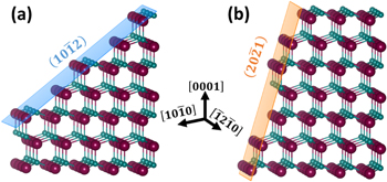
Figure 1. Schematic of the ZnO crystal structure along the Zn-polar c-axis and cut parallel to the (a)  and (b)
  planes. The small green (resp. large purple) spheres represent the Zn-atoms (resp. O-atoms).
Download figure:
Standard image High-resolution imageThe structural morphology of the  and
and  ZnO single crystal surfaces, after the thermal annealing, is shown by AFM images in figures 2(a) and (b), respectively. In both cases, the surface is smooth and atomically flat while no step edges are observed. The parallel stripes on the
  face are formed during the thermal annealing, probably due to surface instabilities. Both surfaces are eventually of high quality, and only exhibit
  or
or  facets. The root mean squared roughness of the
  and
and  ZnO single crystal surfaces is 2 and 9 Å, respectively.

Figure 2. 2 × 2 μm2 AFM images of the (a)  and (b)
  ZnO single crystal surfaces.
Download figure:
Standard image High-resolution image3.2. Structural morphology of ZnO nanostructures grown by CBD
3.2.1. SEM
The morphology of ZnO grown by CBD on the  and
and  ZnO single crystals is shown by top-view and cross-sectional FESEM images in figures 3(a)–(h). On both
  and
and  surfaces, a nanostructured layer is formed and the nanostructures appear to be uniformly tilted with respect to the substrate surface. The tilt angle between the growth direction and substrate surface was measured on more than 30 nanostructures by using cross-sectional FESEM images as presented in figures 3(c), (f) and (h), which were analyzed by ImageJ software.

Figure 3. Top- and cross-sectional-view FESEM images of ZnO grown by CBD under identical conditions on both semipolar ZnO single crystals. (a)–(c) ZnO NWs on top of the  ZnO single crystal. (b) is a high magnification image of (a). (d)–(h) ZnO nanostructures on top of the
  ZnO single crystal. (e) and (g) are high magnification images of (d) on un-coalesced and coalesced regions, respectively. (c), (f), and (h) are the cross-sectional-view images corresponding to (b), (e), and (g) top-view images, respectively.
Download figure:
Standard image High-resolution imageElongated ZnO nanostructures are grown on top of the  ZnO single crystal, exhibiting hexagonal shapes with relatively well-defined top facets and sidewalls, which are typical of ZnO NWs, as revealed in figures 3(a)–(c). The ZnO NWs cover the whole substrate surface with a high number density of 56 ± 3 μm−2. Their average length and diameter are about 315 nm and 60 nm, respectively, corresponding to an aspect ratio of about 5. The length distribution of nanostructures is relatively narrow, while a broad range of diameters occurs, as observed in figures 3(a) and (b). The nanostructures with a diameter larger than 100 nm likely result from coalescence effects due to the high nucleation rate. Their growth direction is uniform and tilted with respect to the substrate surface by an angle of 47.6 ± 1.4°, as shown in figure 3(c), implying that all ZnO NWs grow along the same direction. The present tilt angle corresponds to an angle of 42.4 ± 1.4° between the normal to the growth direction and the
  top surface plane, which is remarkably close to the 42.77° angle between the c-planes and
  planes of ZnO. This strongly suggests that the ZnO nanostructures grow along the polar c-axis. The top facet of ZnO NWs also appears perpendicular to the growth direction, and should accordingly be polar c-planes. Additionally, the sidewalls of ZnO NWs are parallel each other, indicating an in-plane orientation and a possible homoepitaxial growth.
A distinct growth behavior is observed on the  ZnO single crystal, as presented in figures 3(d)–(h). The low magnification FESEM image in figure 3(d) reveals the formation of a 2D layer with a low structural uniformity through the occurrence of distinct regions. A layer composed of elongated ZnO nanostructures, growing on the
  surface, is observed on the high magnification FESEM images shown in figures 3(e) and (f). The ZnO nanostructures have a typical length and diameter of about 390 nm and 110 nm, respectively. The broad range of diameter is the result of the high nucleation rate and of coalescence effects. The growth direction of the elongated ZnO nanostructures is uniformly tilted with respect to the substrate surface by an angle of 14.5 ± 1.5°, as shown in figure 3(f). The corresponding 75.5 ± 1.5° angle between the normal to the growth direction and the
  top surface plane is very close to the 74.88° angle between the c-planes and
  planes of ZnO. This strongly indicates again that the elongated ZnO nanostructures grow along the polar c-axis. In contrast, other regions, as shown in figures 3(g) and (h), reveal the formation of a compact 2D layer with a significant roughness and a thickness of 210 nm. This likely originates from the coalescence of the previously observed elongated nanostructures. Interestingly, the smooth parts of the 2D layer top surface are parallel to the substrate surface and should therefore exhibit
  semipolar planes. The formation of
  semipolar planes is expected to be driven by thermodynamic considerations. The textured surface formed by the highly dense ZnO nanostructures shown in figures 3(e) and (f) is composed of the low surface energy m-planes and the high surface energy c-planes [25]. As growth proceeds, the formation of the
  surface is favored by reducing its total surface energy as (i) the formation of a planar layer decreases the specific surface area, and (ii) the surface energy of the
  plane is expected to be lower than that of the c-plane. The distinct regions formed on the
  surface are likely due to inhomogeneities in the surface structural properties, leading to a local variation of the nucleation rate and hence to the formation of distinct elongated nanostructures or of a compact 2D layer.
In order to control the nucleation density and to clearly identify the morphology of ZnO nanostructures grown on the  ZnO single crystal, a SAG was performed by patterning the
  surface with EBL. A low density of holes in the pattern was used along with a reduced growth time of 1 h to prevent coalescence effects resulting in the formation of a compact 2D layer. Top-view FESEM images of the SAG of ZnO by CBD are shown in figures 4(a) and (b). ZnO NWs clearly nucleate and grow from the holes in the pattern with high structural uniformity. Their average length and diameter are 1.6 μm and 330 nm, respectively, corresponding to an aspect ratio of about 5. No ZnO NWs are found to grow outside the holes, confirming that the PMMA layer efficiently inhibits the ZnO NW nucleation. The ZnO NWs appear to lie down on the substrate surface, similarly to the spontaneous growth on the
  ZnO single crystal. All the ZnO NWs exhibit parallel m-plane sidewalls, revealing an in-plane orientation. The high uniformity over the whole domain further confirms that ZnO NWs effectively form on the
  surface, even though this semipolar plane is highly tilted with respect to the polar c-plane.

Figure 4. (a) Low and (b) high magnification top-view FESEM images of ZnO NWs grown by CBD on top of the patterned  ZnO single crystal.
Download figure:
Standard image High-resolution imageBoth  and
and  semipolar ZnO surfaces are eventually of high chemical activity with regards to the growth of ZnO NWs by CBD. The FESEM images suggest that an homoepitaxial growth occurs with an elongation along the c-axis, resulting in uniformly tilted ZnO NWs.
3.2.2. HRXRD and x-ray pole figures
2Theta/omega scans, omega scans and x-ray pole figures were collected in order to confirm the homoepitaxial growth of ZnO NWs and nanostructures along the polar c-axis on top of the  and
and  ZnO single crystals. The 2Theta/omega scan of the bare
  and
and  ZnO single crystals, as presented in figures 5(a) and (d), reveal high intensity diffraction peaks pointed at 47.554° and 69.066°, respectively, which is in excellent agreement with the positions of the
  and
and  diffraction peaks at 47.539° and 69.100°, respectively, as reported in the 00-036-1451 ICDD file of wurtzite ZnO. Both
  and
and  diffraction peaks are sharp, with a full-width-at-half-maximum (FWHM) of 0.014° and 0.023°, respectively. After the growth of ZnO NWs on top of the
  ZnO single crystal, the peak position at 47.535° and FWHM of 0.010° are not significantly changed, suggesting their homoepitaxy, while a slight broadening is observed at the base owing to the small dimensions of the ZnO NWs. Similarly, after the formation of a coalesced layer of elongated ZnO nanostructures on top of the
  ZnO single crystal, the
  diffraction peak remains largely unchanged with a peak position of 69.083° and a FWHM of 0.018°, suggesting the high crystalline quality and homoepitaxy of the coalesced ZnO layer.
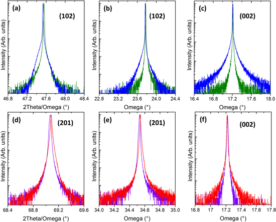
Figure 5. (a)–(c) HRXRD patterns of the bare  ZnO single crystal (in green) and of ZnO NWs grown by CBD on top of the
  ZnO single crystal (in blue). (d)–(f) HRXRD patterns of the bare
  ZnO single crystal (in purple) and of ZnO nanostructures grown by CBD on top of the
  ZnO single crystal (in red). (a), (d) 2Theta/omega scans recorded on the
  and
and  diffraction peak, respectively. (b), (c), (e), (f) Omega scans recorded on the

 and
and  diffraction peak, respectively.
Download figure:
Standard image High-resolution imageThe omega scans recorded on the  and
and  diffraction peaks for the ZnO NWs grown on top of the
  ZnO single crystal, as presented in figures 5(b) and (c), show a FWHM as low as 0.005° and 0.008°, respectively, which is in the same range as the bare
  ZnO single crystal with a FWHM of 0.007° and 0.008°, respectively. For both omega scans, the rocking curve is slightly broader at the base, revealing that the ZnO NW orientation is slightly more dispersed as compared to the single crystal substrate. Similarly, the omega scans recorded on the
  and
and  diffraction peaks for the coalesced ZnO nanostructures on top of the
  ZnO single crystal, as presented in figures 5(e) and (f), both show a narrow 0.009° FWHM, in the same range as the 0.012° FWHM of the bare
  ZnO single crystal. A small broadening is only noticeable on the omega scan recorded on the
  diffraction peak. In both cases, the omega scans reveal an excellent ordering and structural uniformity of the ZnO NWs and nanostructures along the growth direction, strongly suggesting an homoepitaxial growth on the
  or
or  ZnO single crystal substrate.
The x-ray pole figure of ZnO NWs on top of the  ZnO single crystal recorded on the
  diffraction peak, as shown in figures 6(a) and (b), reveals one very high intensity peak located at χ = 42.9°, as expected from the
  orientation of the ZnO single crystal substrate. The FWHM is as low as 2.2°, confirming the high crystallinity of the ZnO substrate and NWs. Three additional minor diffraction peaks, located at χ = 70.1°, 47.0°, and 70.0°, correspond to the
 and
and  reflections, respectively. They occur due to the resolution limit of the x-ray source and to the possible sample misalignment, leading to slight deviations from the
  diffraction conditions. The x-ray pole figure recorded on the
  diffraction peak, as presented in figures 6(c) and (d) reveals the expected high intensity peak at the center with a 1.6° FWHM, and its associated equivalent reflections with lower intensity located at χ = 39.9° and 72.3°. Therefore, for both x-ray pole figures, the expected diffraction peaks corresponding to the
  ZnO single crystal substrate are visible. Since no other significant reflections occur, the ZnO NWs grown on the substrate surface are expected to have homoepitaxially nucleated.
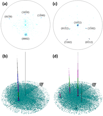
Figure 6. (a), (c) 2D and (b), (d) 3D x-ray pole figures of ZnO NWs grown by CBD on top of the  ZnO single crystal and recorded on the (a), (b) ZnO
  and (b), (c)
  diffraction peaks, respectively.
Download figure:
Standard image High-resolution imageSimilarly, x-ray pole figures of ZnO nanostructures on top of the  ZnO single crystal were recorded on the
  and
and  diffraction peaks, as shown in figures 7(a), (b) and (c), (d), respectively. The
  x-ray pole figure reveals one diffraction peak of high intensity at χ = 74.8°, which is as expected for the
  diffraction peak of the
  ZnO single crystal substrate. Three minor diffraction peaks with very low intensity and corresponding to the
  planes are located at χ = 15.5° and 61.2° and occur due to deviations from diffraction conditions. The small 2.0° FWHM of the main diffraction peak is in agreement with the high crystallinity of the ZnO substrate and nanostructures. Since no other reflections are visible, the ZnO nanostructures on top of the
  surface have the same crystallographic orientation as the substrate. This is also confirmed by the x-ray pole figure recorded on the
  diffraction peak, which shows a high intensity peak at the center with a low FWHM of 1.3°. Several lower intensity equivalent reflections occur at χ = 30.5°, 57.6° and 66.7°, while four other minor diffraction peaks corresponding to the
  planes are either located at χ = 32.0° or at χ = 55.5° and occur due to deviations from diffraction conditions.
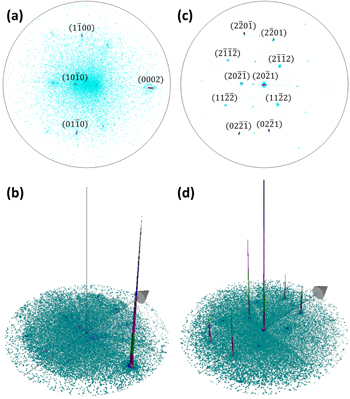
Figure 7. (a), (c) 2D and (b), (d) 3D x-ray pole figures of ZnO nanostructures grown by CBD on top of the  ZnO single crystal and recorded on the (a), (b) ZnO
  and (b), (c)
  diffraction peaks, respectively.
Download figure:
Standard image High-resolution image3.2.3. Raman spectroscopy
The ZnO bulk single crystals and nanostructures are crystallized into the wurtzite structure, belonging to the  space group. According to group theory, the optical modes in the Brillouin zone center are expressed following the irreducible representations: Γopt = A1 + E1 + 2E2 + 2B1 [56]. B1 modes are silent.
  and
and  are non-polar modes, which are Raman active only; they are related to vibrations of the Zn and O sub-lattices, respectively. A1 and E1 modes are polar modes, which are both Raman- and infrared-active. They split into longitudinal optical (LO) and transverse optical (TO) phonon components owing to macroscopic electrostatic forces within the polar crystal [56–58]. A1 phonons are polarized parallel to the c-axis, while E1 phonons are polarized in the basal plane. The Raman scattering spectra of ZnO NWs and nanostructures on both the respective
  and
and  ZnO single crystals are shown in figure 8(a).
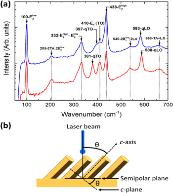
Figure 8. (a) Raman scattering spectra of ZnO NWs and nanostructures grown by CBD on top of the  ZnO single crystal (in blue) and
  ZnO single crystal (in red). (b) Geometry of Raman scattering in the case of ZnO NWs grown along the c-axis on a semipolar surface.
Download figure:
Standard image High-resolution imageThe lines at 100, 332, 410, and 438 cm−1 are assigned to 
 E1(TO), and
  modes, respectively [59]. Second order weak features occur at 205 cm−1 (2TA;
  ), 540 cm−1 (
 2LA), and 663 cm−1 (TA + LO) [59]. Additional lines at higher wavenumber (not shown) include combinations of acoustical and optical modes and overtones. A last couple of lines is observed in both Raman spectra but at slightly different wavenumbers, depending on the substrate orientation. They occur at 397 cm−1 (with a slight overlap with the E1(TO) mode) and at 583 cm−1 in the case of the
  ZnO single crystal substrate. In contrast, they point at 381 and 588 cm−1 in the case of the
  ZnO substrate. In both spectra, the first line is situated between the A1(TO) and E1(TO) modes of bulk ZnO, the second one lying between the A1(LO) and E1(LO) modes [59]. According to Loudon's model for uniaxial crystals, modes with mixed A1 and E1 symmetry character can occur under certain propagation and polarization conditions [57, 58, 60, 61]. For phonon wave vectors parallel or perpendicular to the c-axis, only modes with pure A1 and E1 symmetry can be observed. In contrast, phonon wave vectors with an intermediate direction with respect to the c-axis give rise to mixed symmetry modes; they are termed quasi-modes. Quasi-TO (qTO) and quasi-LO (qLO) modes are observed between the A1(TO) and E1(TO) modes and between the A1(LO) and E1(LO) modes, respectively. Their wavenumber positions are given by the following equations:


where θ is the angle between the phonon wave vector and the c-axis, 

 and
and  are the respective positions of the A1(TO), E1(TO), A1(LO), and E1(LO) modes of bulk ZnO. In the case of the ZnO NWs and nanostructures grown on the
  and
and  ZnO single crystals, the c-axis is inclined with respect to the laser beam propagation direction by an angle θ of 42.77° and 74.88°, respectively. The corresponding Raman scattering geometry is schematically illustrated in figure 8(b). The experimental and calculated positions of the qTO and qLO modes for both ZnO NWs and nanostructures are shown in table 1. The experimental values of the qTO and qLO modes correlate well with the values expected from Loudon's model, which therefore confirms further the orientation of the ZnO substrate and nanostructures with respect to the c-axis. The maximum difference of 2 cm−1 between the calculated and experimental values can be ascribed to small experimental errors and possibly to some small sample misalignment.
Table 1.
Comparison of the experimental positions of the qTO and qLO modes for the ZnO NWs and nanostructures grown on top of the  and
and  ZnO single crystals with the corresponding positions calculated from the positions of pure symmetry modes given by Cuscó et al [59] for ZnO single crystals.
| qTO (cm−1) | qLO (cm−1) | ||||
|---|---|---|---|---|---|
| Angle between the c- and top surface planes (°) | Calculated | Experimental | Calculated | Experimental | |
 ZnO single crystal ZnO single crystal |
42.77 | 396 | 397 | 581 | 583 |
 ZnO single crystals ZnO single crystals |
74.88 | 380 | 381 | 589 | 588 |
4. Discussion
4.1. ZnO NW nucleation and growth on semipolar ZnO surfaces
The combination of cross-sectional FESEM images, HRXRD, x-ray pole figures, and Raman spectra reveal the homoepitaxial nucleation and growth of ZnO NWs by CBD on semipolar ZnO single crystals. Their growth direction is along the c-axis, resulting in a dense, uniform ZnO nanostructured layer tilted with respect to the substrate surface. As in the case of c-planes for ZnO single crystal substrates, the development of the epitaxial nucleus into the NW shape is expected to be driven by surface energy anisotropy [23]. The non-polar m-planes with low surface energy preferentially develop, leading to an elongation of the nucleus along the polar c-axis and thus to the formation of polar c-plane top facets and m-plane sidewalls. The resulting ZnO NWs appear tilted with respect to the semipolar substrate surface. In the case of the  ZnO single crystal, ZnO NWs with well-defined hexagonal shape develop since the angle between the c-axis and
  plane is significant. In the case of the
  ZnO single crystal, the elongated nanostructures develop almost along the substrate surface. The formation of complete hexagonal ZnO NWs with well-defined hexagonal shape is prevented owing to the very small 14.12° angle between the c-axis and
  plane. Instead, the high axial growth rate leads to large coalescence effects between adjacent nanostructures. Eventually, the c-plane top faces with high surface energy vanish and a compact 2D layer exhibiting a
  top face is formed. By using the SAG process and thus controlling the nucleation density on the
  ZnO single crystal, the coalescence is hindered, while the PMMA layer efficiently separates the bottom facet of the developing nucleus and the substrate surface, thus favoring the formation of isolated and tilted ZnO NWs with well-defined sidewalls. The present well-ordered tilted ZnO NWs are of high interest in the fields of optoelectronics and photonics, where the need for exalting specific optical modes requires controlling their period and dimension distribution [62], as well as of piezoelectricity including surface acoustic wave devices and microelectromechanical systems in innovating architectures [63].
4.2. ZnO NW growth on polycrystalline ZnO seed layers
The possibility to grow ZnO NWs on semipolar ZnO single crystals is noteworthy, as it enables further insights into the nucleation and growth of ZnO NW arrays on polycrystalline ZnO seed layers made of NPs. The present NPs act as nucleation sites for a typical range of sizes and show a wide range of crystalline orientations, including non-polar, semipolar, and polar planes [31, 32, 35, 37–41, 43, 64]. The nucleation process and the characteristics of ZnO NW arrays, such as vertical alignment and density, are expected to strongly depend on the relative density and chemical activity of the different types of NPs. The electrostatic interactions between the ZnO NPs and the Zn2+ and OH− active ions in aqueous solution favors the preferential fast nucleation on the charged polar c-plane NPs, while the slower growth on non-polar plane NPs is inhibited owing to competitive effects [23, 31]. The ZnO surface configuration is also critical for the nucleation and growth process. A higher growth rate, correlated to a higher surface reaction rate, was reported for Zn-polar ZnO NWs compared to O-polar ZnO NWs [29]. The distinct chemical activity of the two polar surfaces has notably been explained by the higher surface oxygen dangling bond (DB) density of Zn-polar surfaces compared to O-polar surfaces, by considering that the ZnO surfaces are hydroxylated in aqueous solution and that Zn2+ ions are the limiting reactant for the growth [29, 65, 66]. In the case of semipolar surfaces, different surface charge and configurations are expected, depending on the degree of inclination with respect to the polar c-plane. The intensity of the spontaneous polarization is reduced by a geometrical factor corresponding to the projection on the normal axis to the semipolar surface [65, 67]; additionally, the zeta potential defining the electrical charge of the surfaces is highly dependent upon the crystallographic plane [68–70]. Similarly, the surface oxygen DB density decreases with the degree of inclination. Particularly, the  semipolar surface shows a surface oxygen DB density of 24.1 nm−2, which is slightly lower than that of 32.8 nm−2 for the Zn-polar c-plane ZnO surfaces [65]. In contrast, it is much larger than that of 8.6 nm−2 for the
  surface, which is close to 10.9 nm−2 for the O-polar c-plane ZnO surface and slightly above the non-polar m- and a-planes with a value of 6.8 and 5.9 nm−2, respectively [65]. Following these considerations and the present results, the nucleation on semipolar ZnO NPs is expected to occur owing to their significant chemical activity, particularly when the tilt angle with the c-plane is small, as for
  and
and  semipolar surfaces.
The effects of the crystalline orientation and polarity of the NPs of the ZnO seed layer on the vertical alignment and density of ZnO NW arrays is schematically represented in figure 9. The competitive effects between the NPs should favor the NW nucleation on those with the highest chemical activity (i.e., surface charge and oxygen DB density) in their local environment. In the case of poorly textured (i.e., randomly oriented) ZnO seed layers, as shown in figure 9(a), the NPs have a broad distribution of non-polar, semipolar and polar orientations, without a clear preferential orientation. The ZnO NW nuclei should preferentially form on the polar c-plane NPs, which have a large mosaicity (i.e. the angle of the c-plane with the surface). Their vertical alignment is thus not optimal. Moreover, a high nucleation rate is also expected on the semipolar plane NPs owing to their significant density, leading to highly tilted ZnO NWs. The nucleation on non-polar plane NPs is inhibited, even though they have a high relative density, because of their low chemical activity. The resulting ZnO NW array is made of NWs that nucleated on NPs with different crystalline orientations, and thus display a poor uniformity and vertical alignment as well as a fairly low density [31]. In the case of a highly textured ZnO seed layer along the c-axis, as shown in figure 9(b), the ZnO NWs preferentially nucleate and grow on the polar c-plane NPs, which have a much smaller mosaicity favoring the vertical alignment. In contrast, their nucleation should largely be inhibited on the semipolar plane NPs owing to their low density and isolated positions between polar c-plane NPs with higher chemical activity. The resulting ZnO NW arrays therefore show a high uniformity and vertical alignment as well as a large density [41, 42]. Eventually, in addition to the NP size, mosaicity, roughness and porosity as reported in the literature [30, 31, 33, 37, 38, 40, 43, 64], it is deduced here that the significant presence of semipolar plane NPs in ZnO seed layers account, to a certain extent, for a decreased structural quality of ZnO NW arrays.

Figure 9. Schematic of the ZnO NW growth by CBD on a (a) poorly and (b) highly textured polycrystalline ZnO seed layer composed of NPs with polar, semi-polar, and non-polar plane orientations.
Download figure:
Standard image High-resolution image
5. Conclusion
In summary, the CBD of ZnO NWs was achieved on  and
and  semipolar ZnO single crystal substrates. A nanostructured layer composed of ZnO NWs with high density is formed on the
  surface, while a 2D compact, nanostructured layer obtained by the coalescence of elongated nanostructures occurs on the
  surface. The CBD performed on a patterned
  surface following the SAG process leads to the formation of isolated ZnO NWs with high structural uniformity, which are further highly tilted with respect to the substrate surface. For both
  and
and  semipolar ZnO single crystals, the growth direction of the ZnO NWs is uniformly tilted with respect to the substrate surface by an angle of 47.6° and 14.5°, respectively, showing their elongation along the c-axis. Structural and optical analyses by HRXRD, x-ray pole figures, and Raman spectroscopy reveal the formation of wurtzite ZnO nanostructures, which have homoepitaxially nucleated on the substrates. The presence of qTO and qLO modes in Raman spectra also appears and their origin and position are accounted for within the Loudon's model. Eventually, both semipolar surfaces are found to be chemically active for the nucleation and growth of ZnO NWs, which highlight the versatility of the CBD technique to form NWs on more original surfaces than common polar c-planes. These findings further provide deep insights into the ZnO NW nucleation and growth on polycrystalline ZnO seed layers using CBD, which enable us to comprehensively elucidate the underlying mechanisms responsible for their nucleation on NPs with a wide range of non-polar, semipolar, and polar plane orientations. The possibility to use semipolar surfaces to control the inclination of ZnO NWs, along with the high structural uniformity achieved with SAG offers new approaches through alternative geometries for their integration into nanoscale devices by design.
Acknowledgments
This work was partly supported by the French Research National Agency through the projects DOSETTE (n°ANR-17-CE24-0003) and ROLLER (n°ANR-17-CE09-0033) and by the Carnot Institute Energies du Futur through the project ECOLED. This research benefited from characterization equipment of the Grenoble INP—CMTC platform supported by the Centre of Excellence of Multifunctional Architectured Materials 'CEMAM' (n°ANR-10-LABX-44-01) funded by the 'Investments for the Future' Program. This work was also partly supported by the French RENATECH network through the CIME-Nanotech and PTA technological platforms in a cleanroom environment.