

Abstract
Ultra-small and monodispersed zinc sulfide nanocrystals (NCs) (d ≤ 3 nm) have been prepared without the use of any surfactants by a synthetic route using benzyl mercaptan as a source of sulfur. The prepared NCs are dispersible in highly polar solvents and display the capability to closely pack-up in a bulky film. The NCs were characterized by TEM, XRD and UV–vis optical absorption as well as by steady-state and time-resolved photoluminescence (PL) spectroscopies. Uniform films of ZnS were spin-coated on glass and ITO-glass substrates using a NCs dispersion in N,N-dimethylformamide. The NCs and the resulting films were characterized by morphological and optoelectronic probing techniques such as AFM, SEM, diffuse reflectance, PL and photoelectron spectroscopy in air. These physical investigations confirmed that the chalcogenide NCs grown by this method have the potential to be utilized directly as photocatalysts and are potentially useful building-blocks/starting materials for the fabrication of semiconductor thin films for optoelectronic applications such as LED, luminescent screens, field effect transistor and solar cells. Insights on the chemistry involved in the NCs growth have been provided revealing that their formation proceeds through a mechanism involving a thioether elimination reaction.
Export citation and abstract BibTeX RIS
1. Introduction
ZnS is an important semiconductor for optoelectronic applications. Key applications of ZnS films include the use as layers in electrodes [1], solar cells [1–6], light emitting devices [7–9], photocatalysts [10–14], photodetectors [15, 16] and piezoelectric devices [17–19]. Several efforts have been undertaken to obtain high quality ZnS layers, especially, by the chemical bath deposition (CBD) [3, 20–22]. Compared to more sophisticated preparative techniques utilized for the synthesis of ZnS films such as ionic layer deposition [23], pulsed laser deposition [9], atomic layer deposition [14], e-beam evaporation [16], techniques such as CBD and spin-coating present clear advantages as they are inexpensive, easy to operate and readily available [24, 25]. However, CBD may suffer some limitations such as low material yields compared to the starting reagents and the production of large amounts of waste solutions [26]. Spin-coating is a key technology in optoelectronics [6] and nanoparticles represent excellent starting material for the preparation of films for optoelectronic devices and other applications by this technique [15, 27–29]. From this perspective, the access to semiconducting nanoparticles through convenient synthetic methods is a fundamental leap in materials science. Previous reports employing standard precipitation techniques to obtain large ZnS nanoparticles (10–150 nm) were indeed not suitable for use in spin-coating and led to inhomogeneous and/or porous films [30, 31]. It is clear that nanoparticles with very small size, a narrow size distribution and high dispersibility are required to produce uniform films. A significant breakthrough in the synthesis of nanoparticles was achieved when group II (Zn, Cd, Hg) chalcogenide quantum dots were first prepared by colloidal growth [32, 33]. This technique was then refined and extended to other materials such as group IV and V chalcogenides [34, 35], transition metal pnictides (e.g. Cd3P2, Zn3P2, Fe3P2, Ta3N5) [36, 37] and to a wide spectrum of metal oxides [38, 39]. Although a precise control of size and shape can be achieved through this method, the synthetic process requires the assistance of long-chain fatty acids or amines as well as of the ubiquitously used trioctylphosphine oxide for stabilizing the nanoparticles and controlling their growth. Nevertheless, for some applications, the presence of the organic shell coating the nanoparticle is definitely undesirable [35]. Indeed, a major advantage in having uncoated nanocrystals (NCs) is that it is possible to use them as starting material to cast homogeneous semiconductor films without employing time-consuming and not always effective ligand exchange procedures [34, 40]. Furthermore, upon removal of the long-chain organic ligand from the NPs surface, the dispersibility in organic solvents might be dramatically reduced [32]. An approach to synthesize semiconducting nanoparticles, that does not account for the use of surfactants, is represented by the non-hydrolytic sol–gel route (NHSG) [41–44]. This method has been successfully utilized for the preparation of several single- and bi-metallic metal oxides of different sizes and morphologies using metal-organic precursors such as acetates, halides, acetylacetonates and alkoxides that react with benzyl alcohol and benzylamine. This kind of reaction usually proceeds via ester or ether elimination pathways [43, 45, 46].
Some methods for the preparation of metal sulfides nanoparticles inspired by the NHSG methodology were explored in the past [47]. Niederberger et al employed benzyl mercaptan (BM) as a source of sulfur and as the reaction solvent, yet in absence of surfactants to control the growth. The particles obtained in this early report were rather large in size (9–18 nm according to the zinc precursor employed) [47]. Based on a different method, La Porta et al [48] prepared smaller ZnS nanoparticles (although no TEM analysis was performed to confirm the morphological nature of the nanoparticles) using thiourea as a source of sulfur and ethylene glycol as the solvent. In both cases, the dispersibility and the possibility to cast a film with the thus-prepared material were not considered. Furthermore, the mechanism of the process of NCs formation was never investigated in detail.
In this work, a surfactant-free protocol using either dibenzyl ether or anisole as the solvent and BM as a source of sulfur was applied to synthesize ZnS NCs that could be regarded as quantum dots given the reduced size approaching the Bohr's radius (rB = 2.5 nm) [49]. With respect to application, the ZnS-NCs prepared according to this method can be considered as virtually bare NCs since they are coated only by a monolayer of BM molecules that are chemically bound to ZnS surface [50–52]. However, if necessary, BM could be removed by a thermal treatment in inert environment [35]. The resulting NCs can be easily dispersed in dry N,N-dimethylformamide (DMF) by ultrasonication, and then cast into film on ITO and glass substrates by spin-coating. NCs grown by this method are thus largely preferable to colloidal NCs for the fabrication of films [53–55], mainly because no trace of bulky organic molecules, that would be detrimental for the electronic properties of the film, are left [35].
In order to evidence the suitable morphological, optical and electronic properties of the NCs and of the resulting film, a physical investigation was carried out and discussed throughout the manuscript. Furthermore, a mechanistic investigation on the formation of ZnS-NCs was conducted suggesting that the formation of the NCs proceeds via a thioether elimination mechanism.
2. Experimental methods
2.1. Synthesis of ZnS-NCs
The synthesis of the ZnS-NCs was carried out by the surfactants-free reaction between the zinc acetate (Zn(OAc)2) precursor and BM as a source of sulfur in dibenzyl ether at 190 °C or in anisole at 125 °C. Briefly, 1.853 g (0.01 mol) of zinc acetate anhydrous 99.9+% metal basis Alfa Aesar was loaded in a Schlenk type flask and added with 30 ml of dibenzyl ether Merck and 2.34 ml (0.02 mmol) of BM 99% (Alfa Aesar), preheated at 100 °C to allow the dissolution of zinc acetate, and then the temperature was increased up to the desired value. An off-white dense precipitate started forming within 1 h. The reaction was carried out for 24 h and then allowed to cool to room temperature. The pale-yellow precipitate was separated from the supernatant by vacuum filtration using PVDF Durapore membrane filters with 0.22 μm pore size (MILLIPORE). It was washed three times with absolute ethanol and one time with diethyl ether and dried under vacuum overnight. The ZnS-NCs powder was finely crushed by an agate mortar for characterization and to prepare the dispersion. A small aliquot of the solvent containing the reaction sub-products were analyzed by gas chromatography coupled with mass spectroscopy (GC-MS). Using anisole as medium, the reaction was carried out and worked up as in DBE but at 125 °C, a temperature compatible with the boiling point of anisole (153.8 °C). Purified ZnS-NCs result in large yellow chunks with crystalline appearance (see figure S1(a), which is available online at stacks.iop.org/NANO/29/385603/mmedia) that can be reduced in powder by crushing in agate mortar. The blank reactions were carried out as follows: 0.80 ml of BM in 10 ml of dibenzyl ether or 10 ml of anisole were loaded in a Schlenk flask, degassed, flushed with N2 99.999% and kept under a nitrogen atmosphere at 125 °C for one day. After filtration by 0.22 μm PTFE syringe filter, the reaction products were analyzed by NMR and GC-MS. A scheme of the chemical reaction leading to the formation of ZnS-NCs is portrayed in figure 1 (upper scheme).
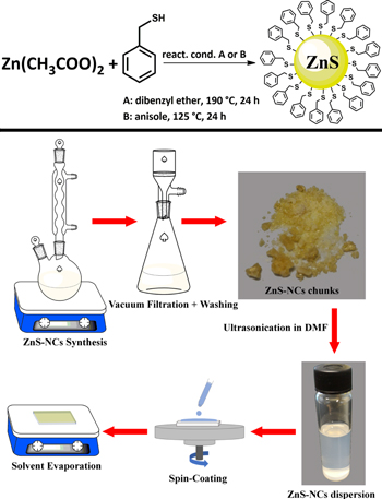
Figure 1. Schematic description of the reaction leading to the formation of ZnS-NCs (upper scheme) and of the steps involved in the ZnS-NCs synthesis and thin-film fabrication (bottom scheme).
Download figure:
Standard image High-resolution image2.2. Thin-film deposition
The dispersion was prepared by ultrasonicating in a glass vial, for 1 h, 50 mg of the purified ZnS-NCs powder in 5 ml N,N-dimethylformamide RE grade from QRëC dried on molecular sieves. The dispersion was allowed to settle down overnight and the supernatant, containing highly dispersed NCs, was separated from the precipitate and used for the morphological and optical characterizations and for the deposition of the ZnS film.
ZnS films were deposited by spin-coating 70–100 μl of the dispersion at 2000 rpm on borosilicate glass and on ITO coated glass substrates and dried on a hot plate at 60 °C for 30 min. The substrates were previously cleaned by subsequent sonication in deionized water, acetone and isopropyl alcohol for a minimum of 10 min each before being exposed to UV-ozone for 10 min immediately prior to film deposition. Drop casting of ZnS film was carried out by dropping the DMF dispersion on the cleaned borosilicate substrate and heating at 60 °C to accelerate the evaporation of the solvent. A scheme of the steps involved in the preparation of the ZnS film is depicted in figure 1 (bottom scheme).
2.3. Morphological study
Powder x-ray diffraction (PXRD) patterns were acquired on purified ZnS-NCs powder by using a Bruker Discovery D8 diffractometer in powder configuration using the rotating sample with anti-air scatterer options without slit. The powders were finely ground in an agate mortar prior the measurement to avoid preferential orientation features in the diffraction pattern.
Aberration-corrected high-angle annular dark-field scanning transmission electron microscopy (HAADF-STEM) was performed on a Titan G 60–300 CT electron microscope at an accelerating voltage of 300 kV. The electron gun was used in the unfiltered mode, and the probe size during STEM analysis was estimated to be approximately 0.5 nm with a beam current of 0.08 nA. A camera length of 360 mm and a condenser aperture size of 50 mm were used for imaging. Additional high resolution transmission electron microscopy (HRTEM) images were acquired by a JEOL ACCELARM JEM-ARM200F transmission electron microscope. TEM samples were prepared by dropping the NCs dispersion in DMF on 200 nm mesh CF200-CU copper coated carbon grids by Electron Microscopy Sciences and drying by a N2 flow followed by overnight vacuum treatment.
SEM images of ZnS film were acquired on the film prepared by spin-coating the ZnS-NCs dispersion in DMF on ITO glass by using a JEOL JSM-7610F field emission scanning electron microscope. AFM images of the ZnS-NCs film were acquired by using a Park Systems NX10 atomic force microscope. The film was obtained by spin-coating on borosilicate glass slide the NCs dispersion in DMF.
2.4. Optoelectronic investigation
Optical absorption and steady-state/time-resolved photoluminescence (PL) measurements were performed on the ZnS-NCs dispersion and film respectively. However, due to a larger thickness of the film, better results in terms of intensity were obtained when PL and diffuse reflectance measurements were taken on a drop-cast film. UV–vis spectra of ZnS-NCs were acquired by a Perkin Elmer Lambda 1050 spectrometer equipped with an integrating sphere for total reflectance measurements. The ZnS-NCs dispersion in DMF was measured in transmission mode using a quartz cuvette. Similarly, absorption measurements of ZnS thin films were acquired in transmission mode by placing the film deposited on glass substrate in the optical path. Diffuse reflectance spectra of the ZnS thin-film deposited on glass were acquired using the same instrument though by placing the substrate in the port of the integrating sphere (diffuse reflectance mode).
Steady-state and time-resolved PL measurements were performed by an Edinburgh Instruments FLS 980 Spectrometer. Steady-state PL spectra of the ZnS-NCs dispersion and of the film were acquired using monochromatic excitation light at 300 nm and a photomultiplier detector for emitted light. The PL-decay was measured at 440 nm (maximum of intensity) using a pulsed laser source emitting at 370.8 nm, with a signal which was deconvoluted from the signal of the source by measuring the decay of a colloidal silica dispersion (LUDOX HS-40 Sigma Aldrich) 10% in water. The lifetime of the electronic state was estimated by a double exponential fit of the experimental data (equation (S1)) and evaluating the time constant τ in terms of averaged time constant τavg as in equation (S2).
Photoelectron spectroscopy in air (PESA) were performed by a RKI AC-2 photoelectron spectrometer on ZnS-NCs film deposited on ITO glass by spin-coating. The edge of valence band was evaluated from the onset of the electron emission yield (square root of electron counts) obtained through linear fitting.
2.5. Mechanistic studies
The mechanistic studies were carried out by analyzing the GC-MS of the reaction products separated from the NCs by filtration with a membrane filter. Briefly, 100 μl of the resulting reaction products were filtered by 0.46 μm pore membrane syringe filter and diluted in 3 ml of dichloromethane (Honeywell HPLC grade) and analyzed by a gas chromatography equipment Perkin-Elmer Clarus 680 GC coupled with Clarus SQ 8 T mass spectrometer (GC-MS). The injection temperature was set at 60 °C for identifying also the lightest compounds, while the oven temperature was set to 100 °C.
Further experimental details are reported in the supplementary material.
3. Results and discussion
The NCs were prepared according to the procedure reported in the experimental section and depicted in figure 1 (upper scheme). When purified and dry, they tend to agglomerate in large yellow crystals (bottom-up assembly) [56] (figure S1(a)) resembling bulk ZnS. This behavior is due to the extremely reduced size and the absence of a bulky organic coordinating shell. However, with the assistance of ultrasonication, ZnS-NCs could be dispersed in highly polar aprotic solvents such as N-methyl pyrrolidinone and N,N-dimethylformamide. These solvents are well known for their ability to disperse various nanostructures, including carbon nanotubes bundles and other carbon nanostructures, thanks to their tendency to form coordination shells [57, 58]. Combining these two properties, it was possible to prepare NCs dispersions and to spin-coat a thin-film suitable for morphological and optoelectronic characterization, as well as, in perspective, for future technological applications. It is important to use dry DMF to avoid the degradation of the as-prepared ZnS-NCs that are not protected by long-chain stabilizing molecules. An image of ZnS-NCs dispersion is reported in figures 1 and S1(b). It was observed that the suspension remains stable for months with no precipitation.
ZnS-NCs were characterized by HRTEM using the aberration-corrected scanning TEM mode (HAADF-STEM). A HAADF-STEM image of the NCs assembly is shown in figure 2(a) and a normal HRTEM image is shown in figure S2. Here NCs appear partially agglomerated after the solvent evaporation. A better outline of the NCs can be observed in the inset of figures 2(a) and of figure S2 where a single NC is magnified allowing us to see the atomic planes of the Würtzite crystal with the c-axis parallel to the plane of the image. The results of a statistical size analysis over a large number of NCs is reported as a histogram in figure 2(c). The NCs diameter distribution is centered at 3 nm and does not exceed 4.5 nm. This result is confirmed by PXRD patterns (figure 3(b)) that evidence very broad diffraction peaks corresponding to small-sized ZnS-NCs. By using the Debye–Scherrer formula D = kλ/Bcos θ, where B is the full width at half maximum of the Miller indexes, λ = 1.540 60 Å (Cu Kα) is the x-ray wavelength, k = 0.94 is the shape factor for cubic crystals and θ is the Bragg angle. A diameter of D = 2.7 nm was estimated. This value is slightly smaller than the D value obtained from TEM analysis due to the fact that it estimates the coherent domain which is always smaller than the actual particle size. Application of the Debye–Scherrer formula to the PXRD pattern of ZnS-NCs synthesized in anisole provides a substantially lower diameter D = 2.1 nm (figure 3(b)), probably, as an effect of the lower reaction temperature (vide infra). The characteristic position and intensity of the {111}5, {220} and {331} reflections are observed by PXRD and selected area electron diffraction (SAED) (figure 2(b)) which shows that the ZnS-NCs have the Würtzite crystalline structure [56].
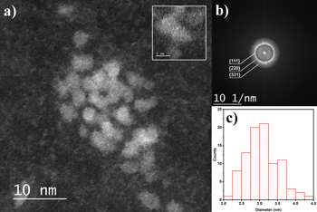
Figure 2. (a) Aberration-corrected high-angle annular dark-field scanning transmission electron microscopy (HAADF-STEM) image and, in the inset, high magnification HAADF-STEM images of a few NCs with different orientation of the z axis. (b) SAED pattern of a single ZnS-NC. The three main reflections have been labeled with their relative Miller indexes; with crystallographic c-axis lying parallel to the image plane; (c) histogram of the statistical size analysis of NCs done on several HRTEM images.
Download figure:
Standard image High-resolution image
Figure 3. Powder XRD pattern of ZnS-NCs synthesized in (a) dibenzyl ether and (b) anisole media.
Download figure:
Standard image High-resolution imageThe optical absorption spectra of ZnS-NCs shown in figures 4(a) and (b) for dispersion in DMF and drop-cast film, respectively, reveal the typical absorption edge of semiconducting NCs with the excitonic peak blue-shifted with respect to bulk ZnS. In this case, the excitonic peak is not well defined as in the case of ligand-coated NCs [32, 33], probably due to a higher surface exciton recombination rate that quenches the excited state caused by the absence of the ligand and by a partial agglomeration [52]. The energy of the 1Sh → 1Se electronic transition between the molecular-like discrete electronic levels was estimated to be, from the onset of the Tauc plot, Eg(R) = 3.71 eV (figure 4(c)). Tauc plot was traced by measuring the diffuse reflectance (Kubelka–Munk function) of the NCs drop-cast film performed by an integrating sphere. Eg(R) is, as expected, slightly blue-shifted due to quantum confinement effect from the bulk band-gap energy of Eg = 3.68 eV. This value is also in a good agreement with the E(r) predicted by the theory (Brus' equation [59] (equation (1))). Using rNC = 1.5 nm (dNC = 3 nm) obtained from TEM images statistical analysis, see histogram in the inset of figure 2(c), a 1Sh → 1Se optical transition energy Eg (r) = 3.74 eV was obtained

where Eg is the bulk ZnS band-gap,  is the reduced Planck's constant, e is the electron charge, ε is the dielectric constant of bulk ZnS and μe, expressed as follows

is the semi-empirical expression for the size-dependent effective mass of the electron [60], where me is the mass of the electron. This value is very close to the experimental 3.71 eV obtained by the Tauc plot.
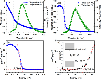
Figure 4. (a) UV–vis absorption (blue dots) and steady-state PL (green dots) spectra of ZnS-NCs dispersion in DMF. (b) UV–vis absorption (blue dots) and steady-state PL (green dots) spectra of ZnS-NCs drop-cast on a fused silica substrate. (c) Tauc plot of the drop-cast ZnS-NCs on fused silica substrate. (d) PESA spectrum of a ZnS-NCs powder. The inset shows the energy level diagram based on the ionization potential obtained from PESA (for 1Sh level) and optical gap from UV–vis measurements.
Download figure:
Standard image High-resolution imagePL measurements of solution and powder shown in figures 4(a) and (b) highlight the good emissive properties of the material. For ZnS-NCs dispersion in DMF, the PL peak is centered at 440 nm while for the powder is slightly red-shifted to 446 nm. This small shift can be caused by the close packing of the NCs resulting in an electronic coupling between the NCs and thus in an overlap of the wavefunctions [56]. Based on PL-decay measurements shown in figures S3 and S4, the electronic state lifetime was estimated. Through fitting the experimental data with a double exponential function, the average time constants τdisp = 3.04 ns and τfilm = 1.49 ns were found, respectively, for NCs dispersion and film. These values of τ are the weighted average values of the two-time constants occurring in the biexponential formula used to fit the experimental data (equation (S1) in supplementary data). Although these time constants are of the same order of magnitude, the lifetime for NPs in solution is slightly longer than for the NPs in the thin-film. The small difference between the two PL-decay curves lies mostly in the difference between the fast components which are originated from the surface defects-related non-radiative decay [61, 62], which effectively leads to a more pronounced quenching due to stronger NC–NC interactions in the film [52]. On the contrary, there is no significant difference between the slow components assignable to the non-radiative decay occurring in NC core which are originated from material non-stoichiometries and vacancies [61] and, to a lesser extent, from phonon–electron scattering, not particularly significant in direct gap semiconductors such as ZnS [63]. It is worth to notice that the lifetime of the electronic state is in the one nanosecond scale, thus in the order of magnitude of PL-enhanced Mn2+:ZnS-NCs [64]. On the other hand, as expected, PL-lifetime is one order of magnitude lower (i.e., faster decay) than NCs coated with organic molecules or by a layer of inorganic material (core–shell structure), both acting as surface defects passivators [65–68]. If desired, a PL-lifetime extension can be eventually obtained by carrying out a suitable post-synthetic ligand exchange with long-chain molecules [69] or by coating NCs with a passivating inorganic layer (core–shell) [70].
From the onset of the photoelectron yield spectrum measured with PESA, the 1Sh electronic level of the film was found to be −5.70 eV respective of the vacuum level. Nevertheless, ZnS-NCs in powder form measured by PESA show a 1Sh level of −5.90 eV, hence closer to literature values. We consider this value more reliable since the measurement on thin-film might have been affected by the influence of the underlying ITO substrate, given the extremely thin nature of the film. PESA curve of ZnS-NCs powder with relative linear fit are presented in figure 4(d). By adding the optical gap energy obtained from diffuse reflectance measurements (Tauc plot in figure 4(c)), the energy of the 1Se level has been calculated to be −2.19 eV respective to the vacuum level. For clarity, a scheme of the band-gap related electronic levels of ZnS-NCs is shown in the inset of figure 4(d). Both 1Sh and 1Se molecular-like states (originated from bulk valence and conduction bands respectively) are, when compared to literature values of bulk ZnS [71] and ZnS-NCs [72], shifted toward the vacuum level, i.e., toward less negative energies. However, considering that photoelectron spectroscopy performed in air may provide results that differ from measurements done in ultrahigh vacuum (using ultraviolet photoelectron spectroscopy, UPS), a reference work-function measurement of a gold standard by PESA is also performed, providing EWF(Au) = 4.72 eV (4.78 eV for PESA literature value [73]), versus EWF(Au) = 5.1 eV obtained from UPS measurements [74].
Morphological analysis of ZnS films deposited by spin-coating from NCs dispersions was carried out by scanning electron microscopy (SEM) and by atomic force microscopy (AFM). SEM images of the ZnS film deposited on ITO glass are shown in figure S5 of the supporting information. Figure S5(a) is relative to films deposited from ZnS-NCs synthesized at 190 °C in DBE whereas figures S5(b) and (c) are relative to a film fabricated from ZnS-NCs synthesized at 125 °C in anisole. In the first case, the film has a quite elevated roughness, and the presence of large NCs agglomerates lying on the film surface is evident. In the second case, when a dispersion of smaller NCs synthesized at 125 °C in anisole is used, the film appears much more uniform and composed of 20–30 nm NCs island-like grains (see figure S5(c)) and without NCs agglomerates on the surface. This is confirmed by AFM topography shown in figures S6(c) and (d) of supporting data. Agglomerations confer to the film a roughness of Ra = 6.8 nm comparable to, if not better than, ZnS films obtained by CBD [22, 75, 76] and oxides films cast from NCs dispersion [53–55]. On the other hand, when larger NCs are used, namely NCs synthesized at 190 °C in DBE, the film has a roughness of Ra = 15 nm (figures S6(a) and (b)). It is thus clear the NCs size plays a fundamental role on their dispersibility and consequently on the quality of the resulting film. Therefore, these measurements highlight the suitability of this method for casting ZnS films starting from a ligand-free NCs dispersion. We anticipate that this method can be applied to chalcogenides in general and it appears particularly suitable for the fabrication of optoelectronic devices such as luminescent screens, LED, transistors and solar cells.
The mechanism of the reaction leading to the formation of the ZnS-NCs was investigated by the analysis of the reaction products formed in solution by GC-MS (from figures S7 to S10). The fact that similar ZnS-NCs could be prepared in both DBE and anisole with a yield close to 100% suggest the absence of a specific role of the solvent on the reaction pathway.
It is well known that the formation of metal oxides in the NHSG can proceed via halide, ether, ester or aldol elimination [45, 46]. Yet, concerning the synthesis of ZnS-NCs by the thio-sol–gel route, as previously suggested by Niederberger et al [47], the formation of a thioacetic ester in the reaction of Zn(OAc)2 and BM would lead to ZnO rather than ZnS. The replacement of the acetate ligands by molecules of BM, the formation of zinc benzyl thiolate as intermediate and the subsequent elimination of dibenzyl sulfide would initiate the formation of the growing ZnS chain according to the thioether elimination mechanism depicted in scheme

Scheme 1. Plausible ZnS-NCs formation pathways: (top) via reaction of benzyl mercaptan with Zn(OAc)2 followed by the elimination of dibenzyl sulfide (bottom) (b) as an effect of the in situ formation of H2S by the condensation of two molecules of benzyl mercaptan.
Download figure:
Standard image High-resolution image
Indeed, GC-MS analysis of the reaction mixture following the synthesis of ZnS-NCs in anisole at 125 °C (figure S7) shows the formation of dibenzyl thioether as the main reaction product along with minor amounts of dibenzyl disulfide. The latter product is likely to arise from the coupling of two molecules of dibenzyl thioether. No traces of thioacetic ester were found. Furthermore, when a blank reaction was carried out by dissolving BM in anisole under identical conditions as per the synthesis of ZnS-NCs but in the absence of Zn(OAc)2, no formation of dibenzyl thioether was observed (figure S8). This observation demonstrates that the latter compound is generated as an effect of the reaction of BM with Zn(OAc)2 leading to the formation of ZnS. The GC-MS chromatogram of the reaction mixture from the synthesis of ZnS-NCs in dibenzyl ether (figure S9) is more complex and less clean than for the corresponding reaction in anisole. Dibenzyl thioether is, however, the main product. Dibenzyl disulfide, trisulfide and several oxidation products of the various thio- compounds are also found in the reaction mixture. The formation of the latter series of compounds is likely to arise from the higher reaction temperatures employed when compared to the analogous synthesis in anisole. Interestingly, the chromatogram of the blank reaction carried out in dibenzyl ether under identical reaction conditions as per the synthesis of the ZnS-NCs, but in the absence of Zn(OAc)2 (figure S10), shows the formation of small amounts of dibenzyl thioether, disulfide and trisulfide even in the absence of Zn(OAc)2. The formation of dibenzyl disulfide and trisulfide in dibenzyl ether at 190 °C is supposed to take place due to the presence of H2S originated from the condensation of two BM molecules as in scheme
4. Conclusions
In conclusion, ZnS-NCs have been synthesized by a ligand-free thiol-based synthesis obtaining surface uncoated ZnS-NCs. This method allowed us to obtain very small NCs (d ≤ 3 nm) that show quantum confinement effects given the reduced size. The reduced size also allowed the preparation of stable dispersion of the NCs in polar organic solvents that can be deposited on suitable substrates by spin-coating. A morphological and optoelectronic characterization of the NCs and of the resulting film was carried out demonstrating that NCs prepared by this method can be effectively utilized as building-blocks for the deposition of semiconducting material thin-films for optoelectronic applications circumventing the problem of organic ligand exchange or removal. Furthermore, this method has the potential to be extended to other more relevant optoelectronic materials in the future. Finally, the mechanism of ZnS-NCs growth was also elucidated by analyzing the reaction sub-products through NMR and GC-MS techniques. A main reaction mechanism involving the initial formation of a zinc benzyl thiolate with thioether elimination was identified.
Acknowledgments
The authors would like to thank the Frontier Research Center (FRC) of VISTEC for support of characterization instruments and, in particular, Somlak Ittisanronnachai for TEM measurements and technical support for SEM. S D G and V D E would like to thank the Thailand Research Fund (Grant No. RSA6080059) for funding this research. P P would like to acknowledge the funding from the Office of the Higher Education Commission (OHEC) and the Thailand Research Fund (TRF) under Grant No. MRG5980214.