

Abstract
It is challenging to hierarchically pattern high-aspect-ratio nanostructures on microstructures using conventional lithographic techniques, where photoresist (PR) film is not able to uniformly cover on the microstructures as the aspect ratio increases. Such non-uniformity causes poor definition of nanopatterns over the microstructures. Nanostencil lithography can provide an alternative means to hierarchically construct nanostructures on microstructures via direct deposition or plasma etching through a free-standing nanoporous membrane. In this work, we demonstrate the multiscale hierarchical fabrication of high-aspect-ratio nanostructures on microstructures of silicon using a free-standing nanostencil, which is a nanoporous membrane consisting of metal (Cr), PR, and anti-reflective coating. The nanostencil membrane is used as a deposition mask to define Cr nanodot patterns on the predefined silicon microstructures. Then, deep reactive ion etching is used to hierarchically create nanostructures on the microstructures using the Cr nanodots as an etch mask. With simple modification of the main fabrication processes, high-aspect-ratio nanopillars are selectively defined only on top of the microstructures, on bottom, or on both top and bottom.
Export citation and abstract BibTeX RIS
1. Introduction
The integration of high-aspect-ratio nanostructures into microstructures to form multiscale hierarchical nanostructures has drawn great interests in many applications including biomedical detection [1], mixture separation [2], liquid-repellence [3], and lab-on-a-chip devices [4]. However, it is challenging to integrate high-aspect-ratio nanostructures into microstructures. It has been found that photoresist (PR) is not able to uniformly cover on microstructures [5]. Thus, it is difficult to pattern high-aspect-ratio nanostructures on microstructures using conventional lithography techniques which require uniform PR layer coating on the microstructures. Recently, capillary force lithography [6] and nanoimprint lithography [7] have been employed to pattern nanostructures onto microstructures. In both capillary force lithography and nanoimprint lithography, nanofeatures are transferred from rigid molds to polymer surfaces using either capillary force or heat/UV treatment [8]. Thus, it is difficult to pattern hierarchical nanostructures on hard materials or materials with high melting points using these techniques. In addition, it is impossible to pattern nanostructures on the bottom surfaces (trenches) of the microstructures using the capillary force lithography and the nanoimprint lithography techniques because the molds only contact the top surfaces (ridges) of the microstructures. Photolithography can define nanopatterns on the bottom surfaces of microstructures. However, in this case, the microstructures are typically PR materials themselves, defined by photolithography, and should be formed after the nanostructures are made [9]. Thus, this approach is not effective to construct hierarchical nanostructures of the same materials. Alternatively, dip pen lithography has shown the capability to draw oxide patterns on both top and bottom of microstructures [10]. However, dip pen lithography has a relatively low scanning speed which limits the wafer-scale patterning capability [11]. Femtosecond laser two-photon polymerization technique has also shown the capability to pattern arbitrary micro- and nanostructures on selected target substrates, which can be used to pattern hierarchical nanostructures [12]. However, the patterning speed is limited by the laser scanning rate and it takes a long time to pattern on a wafer scale. It is possible to pattern nanostructures on the bottom surfaces of microstructures using bottom-up approaches [13]. However, it is difficult to control the uniformity and regularity of the nanostructures in growth.
Previously, we reported on a soft nanostencil lithography technique, where a free-standing nanostencil membrane was employed for the creation of high-aspect-ratio silicon nanostructures [14, 15]. We also showed that silicon nanopillars could be patterned on the top surfaces of microstructures by the soft nanostencil lithography, whereas the nanostructures could not be patterned on the bottom surfaces of the microstructures due to the 'blurring' effect [16]. In this work, we demonstrate an advanced soft nanostencil lithography technique which can programmatically pattern silicon nanostructures (feature sizes between 200 and 500 nm) selectively either on top of microstructures (feature sizes between 1 and 100 μm) or on bottom, or on both top and bottom with a precise control to form two-tier hierarchical micro/nanostructures. Although the presence of the 'blurring' effect could potentially affect the patterning resolution for the nanostructures, we show that it is possible to control the nanostructure patterning on the bottom surface of microstructures by adjusting the feature size of the nanostencil membrane and the gap distance between the nanostencil and the bottom surface of microstructures.
2. Fabrication scheme
2.1. Nanostructures only on top
Figure 1(a) shows the fabrication schemes of patterning nanostructures only on the top surfaces of the microstructures. First, silicon microgratings are patterned by photolithography and deep reactive ion etching (DRIE). Before removing the PR layer used as an etch mask in the DRIE, a lift-off process is applied to deposit a thin Cr layer only on the bottom surfaces of the microgratings (i.e., microtrenches) (a-i). Then, a soft tri-layer nanostencil membrane, consisting of metal (Cr), PR, and anti-reflective coating (ARC), is transferred onto the microstructured silicon substrate to cover the microstructures. Cr nanodots are deposited on the whole surfaces of the microgratings through the tri-layer nanostencil using e-beam evaporation (a-ii). The nanostencil membrane is then released to result in the Cr nanodots patterns on both top and bottom of the microstructures (a-iii). After that, silicon nanopillars are patterned by DRIE using the Cr nanodots as etch masks. Because the bottom surfaces of the microstructures are fully covered by a thin Cr layer in the previous step (a-i), only the top parts of the silicon microstructures are etched by the DRIE (a-iv). Finally, the Cr etch mask layer is removed by Cr etchant (a-v), resulting in nanostructures only on the top surfaces of the microstructures.

Figure 1. Schematics of selective nanopatterning on microstructured silicon surface. (a) Nanopatterning only the top surface: (a-i) a lift-off process to deposit metal layer only on the bottom surface of microgratings. (a-ii) E-beam evaporation through porous nanostencil to deposit Cr nanodots both on the top and the bottom of the microgratings. (a-iii) Release of the nanostencil mask by NH3/H2O2/H2O. (a-iv) DRIE to create high-aspect-ratio silicon nanopillars only on the top of the microgratings. (a-v) Removal of the Cr layer on the bottom with Cr etchant. (b) Nanopatterning only the bottom surface: (b-i) silicon microgratings (with the photoresist layer still present on top) created by photolithography and DRIE etching. (b-ii) E-beam evaporation to deposit Cr nanodots both on the top and the bottom of the microgratings. (b-iii) Release of the nanostencil by NH3/H2O2/H2O. (b-iv) DRIE to create high-aspect-ratio nanopillars on the bottom surface (i.e., trench). (b-v) Removal of a photoresist layer on the top surface by acetone. (c) Nanopatterning on both the top and the bottom: (c-i) silicon microgratings (with the photoresist layer still present on top) created by photolithography and DRIE etching. (c-ii) Removal of a photoresist layer by acetone. (c-iii) E-beam evaporation to deposit Cr nanodots both on the top and the bottom of the microgratings. (c-iv) Release of nanostencil mask by NH3/H2O2/H2O. (c-v) DRIE to create high-aspect-ratio silicon nanopillars on both the top and the bottom of the microgratings.
Download figure:
Standard image High-resolution image2.2. Nanostructures only on bottom
Figure 1(b) shows the fabrication schemes of patterning nanostructures only on the bottom surfaces of the microstructures. First, the microgratings are patterned by photolithography and DRIE etching (b-i). It should be noted that the PR layer used as an etch mask in the DRIE is still left on the top surfaces of the microgratings for a lift-off process in the later step. Then, a tri-layer nanostencil membrane is transferred onto the microstructures (b-ii). Cr nanodots are deposited through the nanostencil on the whole surfaces of the microstructures using e-beam evaporation (b-iii). After that, the PR layer on the top surfaces of the microgratings is removed by acetone. Thus, the Cr nanodots deposited on the PR layer on the top surfaces of the microstructures is also removed, while the Cr nanodots defined on the bottom surfaces are still retained (b-iv). Finally, DRIE is used to make silicon nanopillars on the bottom surfaces of the microgratings, followed by the removal of the Cr etch mask from the bottom surfaces to result in the nanostructures only on the bottom of the microstructures (b-v).
2.3. Nanostructures on both top and bottom
Figure 1(c) shows the fabrication schemes of patterning nanostructures on both the top and bottom surfaces of the microgratings. First, microgratings are created by photolithography and DRIE etching (c-i). In this case, the PR layer used as the etch mask in the DRIE is completely removed from the microstructured silicon surface (c-ii). A tri-layer nanostencil membrane is then transferred onto the microgratings and Cr nanodots are deposited through the nanostencil onto the whole surfaces of the microgratings using e-beam evaporation (c-iii). After that, the nanostencil membranes are released (c-iv). Finally, DRIE is used to make silicon nanopillars both on the top and the bottom surfaces of the microstructures, followed by the removal of the Cr nanodots (c-v) to result in the nanostructures on both the top and the bottom surfaces of the microstructures.
3. Materials and methods
The micrograting pattern of silicon was prepared by conventional photolithography followed by DRIE, whose details are in the following. A polished silicon wafer was cleaned by Piranha solution (mixture of sulfuric acid and hydrogen peroxide in the volume ratio of 3:1), rinsed by deionized water, and blown by N2 gas. Positive PR (SPR 3012, Shipley Megaposit®) was spun on the silicon wafer with a thickness of 1.8 μm. The wafer was baked on a hotplate at 95 °C for 1 min. It was then exposed by a mask aligner (Karl Suss MA 6) with a soft contact mode. A total of 45 mJ cm−2 dosage was used for the exposure. After that, the substrate was baked on a hotplate at 115 °C for 1 min, followed by developing in MF®-319 developer (Shipley Megaposit®) for 1 min. The silicon substrate was etched using cryogenic DRIE process (PlasmaLab, Oxford Instruments) at −100 °C with SF6 and O2 gases. In this study, the etching depths of 2, 4, and 7 μm were selected for the micrograting structures.
The fabrication and transfer processes of a soft nanostencil has been reported elsewhere [15, 17]. The briefs of the processes are in the following. A polished silicon wafer was cleaned, rinsed, and dehydrated. ARC (XHiRC 16, Brewer Science) was spun on the silicon wafer with a thickness of ∼150 nm. The substrate was baked on a hotplate at 175 °C for 1 min. Negative PR (NR7-1500, Futurrex, Inc.) was spun on top of the ARC layer with a thickness of ∼1.5 μm. It was then baked on a hotplate at 150 °C for 1 min. The substrate was exposed using laser interference lithography to obtain periodic pore patterns [18, 19]. In this study, a He-Cd laser with a wavelength of 325 nm (IK 3501R, Kimmon Koha Co., Ltd) was used with a power of 50 mW. After exposure, the substrate was baked on a hotplate at 100 °C for 1 min. Then, it was developed by RD6 developer (Futurrex Inc.) for 10–12 s. Nanopore patterns with two different pattern periodicities of 580 and 680 nm were made for the nanoporous nanostencils in this study. The ARC layer was etched by reactive ion etching (RIE, Phantom III, Trion Technology) with oxygen plasma. The etch rate of the ARC layer was controlled at ∼3.9 nm s−1. A ∼20 nm thick Cr was deposited on the nanopore patterns after the ARC etching. Then, the nanoporous tri-layer membrane of the Cr/PR/ARC composite films was released from the supporting substrate (silicon) in a NH3/H2O2/H2O solution (1:1:10 in volume). Finally, it was transferred onto microgratings by immersing the microstructured silicon substrate in the solution to be underneath the nanostencil and lifting the substrate to be conformally covered by the nanostencil. In our previous work, both bi-layer nanostencil (PR/ARC) and tri-layer nanostencil (Cr/PR/ARC) were developed [15]. In this study, only tri-layer nanostencil was used due to the higher stiffness over bi-layer nanostencil which is critical to uniformly cover the microstructures without deformation or bending [20]. Because the nanopore patterns of the nanostencil and the microstructures are periodic, fine alignment is not required during the transfer in this study. It is possible to mount the nanostencil on a translational stage and use microscopy to have precise alignment of the nanostencil on the target substrate.
For the hierarchical patterning of nanopillar structures on the microstructures of silicon, cryogenic DRIE process (PlasmaLab, Oxford Instruments) was also used at −100 °C with 30 s etching time, which resulted in the etching depth (i.e., nanopillars' height) of ∼1.5 μm.
All the metal deposition work was performed with an e-beam evaporator (Kurt J Lesker). The deposition rate was ∼0.2 nm s−1.
4. Results and discussion
Figure 2(a) shows an example of the nanostencil membrane placed on the micrograted silicon surface. The tri-layer stencil membrane of the nanopore pattern periodicity of ∼580 nm and the pore size of ∼300 nm is shown in figure 2(a). The color shown from the nanostencil surface is due to iridescence. Below the nanostencil, the square area (1 cm × 1 cm) where the microstructures are defined is also shown. Figure 2(b) shows more details of the placement of the nanostencil over the micrograted surface. As shown in the scanning electron microscope image in figure 2(b), the nanostencil membrane does not collapse or bend into the microtrenches with a spacing of ∼20 μm. In addition, the nanostencil seamlessly contacts the top of the microstructures thus avoiding the 'blurring' effect [21], which will be discussed more later, on the top part.
Figure 2. (a) Photograph of a nanoporous stencil membrane placed on a micrograted surface of silicon. The inset shows the scanning electron microscope (SEM) image of the nanostencil. (b) SEM image of the free-standing nanostencil mask placed on the silicon microgratings with no collapse.
Download figure:
Standard image High-resolution imageFigure 3 shows the fabrication results of the nanopillars created only on the top surfaces of the microgratings (period: ∼60 μm, height: ∼7 μm) using the tri-layer nanostencil membrane (nanopore pattern periodicity: ∼680 nm, pore diameter: ∼420 nm), following the schematic shown in figure 1(a). Figures 3(a) and (b) show that the Cr nanodots were uniformly patterned on both the top (ridge) and the bottom (trench) surfaces of the microgratings, which corresponds to the schematic of figure 1(a-iii). Figures 3(c) and (d) show the silicon nanopillar structures created only on the top surfaces (ridges) of the silicon microgratings after the DRIE using the Cr nanodots as etch masks. In figures 3(c) and (d), the nanodot patterns shown on the bottom surfaces (trenches) of the microgratings are Cr nanodots. Since the bottom surfaces of the microgratings were already fully covered with a thin Cr layer, on top of which the Cr nanodots were additionally deposited through the nanostencil, no silicon nanostructures were formed by the DRIE on the bottom surfaces. The nanopillars created on the top surfaces of the microgratings have a diameter of ∼300 nm and a height of ∼1.5 μm, thus the aspect ratio of ∼5. Figures 3(e) and (f) show the final hierarchical structures of silicon formed after the removal of the Cr layers (the Cr nanodots on the top surfaces as well as the thin Cr layer on the bottom surfaces) using Cr etchant. The result shows that the nanopillar structures can be selectively patterned only on the top surfaces of the microstructures using the proposed scheme (figure 1(a)).

Figure 3. (a) SEM image of the micrograted silicon surface after the deposition of Cr nanodots, corresponding to the schematic of figure 1(a-iii). (b) A higher magnification image of (a). (c) SEM image of the micrograted silicon surface after the DRIE using the Cr nanodots as etch mask, corresponding to the schematic of figure 1(a-iv). (d) A higher magnification image of (c). (e) SEM image of the mirograted silicon surface after the removal of the Cr layers, corresponding to the schematic of figure 1(a-v). (f) A higher magnification image of (e). The scale bar in each image represents 10 μm.
Download figure:
Standard image High-resolution imageFigure 4 shows the fabrication results of the nanopillar structures that were created only on the bottom surfaces (trenches) of the microgratings (period: ∼20 μm, height: ∼2 μm in figure 4(a); period: ∼60 μm, height ∼4 μm in figure 4(b)) using the tri-layer nanostencil membrane (nanopore pattern periodicity: ∼580 nm, pore diameter: ∼250 nm in figure 4(a); nanopore pattern periodicity: ∼680 nm, pore diameter ∼280 nm in figure 4(b)), following the schematic shown in figure 1(b). First, figures 4(a) and (b) show the Cr nanodots patterned only on the bottom surfaces (trenches) of the micrograted silicon surface for the micrograting heights of ∼2 and ∼4 μm, respectively, which correspond to the schematic shown in figure 1(b-iv). The results show that the top surfaces (ridges) of the microgratings are free of Cr nanodots, which were removed by the lift-off process (i.e., when the PR layers on the top surfaces were removed), whereas the bottom surfaces are uniformed covered by the Cr nanodots, regardless of the height of the microgratings. The feature size of the Cr nanodots (∼300 nm) on the bottom surface for the microgratings of 2 μm high is greater than the size of the nanopore of the stencil (∼250 nm) by ∼20%, while that (∼500 nm) on the bottom surface for the microgratings of 4 μm high is greater than the size of the nanopore of the stencil (∼280 nm) by ∼78%. The increase of the feature size is caused by the 'blurring' [21]. For physical vapor deposition (e.g. e-beam evaporation), the scattering of the Cr molecules through the free space (i.e., gap) between the nanostencil and the bottom surface (trench) becomes more significant with a larger gap [22]. Thus the projection area (i.e., size) of the Cr nanodots increases with the height of microgratings. The 'blurring' effect can be reduced by either decreasing the gap size (height of the microgratings) or decreasing the nanopore feature size [23].

Figure 4. (a), (b) SEM images of the micrograted silicon surfaces whose bottom surfaces are patterned with Cr nanodots, corresponding to the schematic of figure 1(b-iv). The micrograting structures shown in (a) and (b) have the heights of ∼2 and ∼4 μm, respectively. (c) SEM image of the micrograted silicon surface (grating height: ∼2 μm) after the DRIE using the Cr nanodots as etch mask, corresponding to the schematic of figure 1(b-v). (d) A higher magnification image of (c). (e) SEM image of the mirograted silicon surface (grating height: ∼4 μm) after the removal of the Cr layers, corresponding to the schematic of figure 1(a-v). (f) A higher magnification image of (e).
Download figure:
Standard image High-resolution imageThen, figures 4(c) and (d) show the silicon nanopillar structures created only on the bottom surfaces of the micrograted silicon surface with the micrograting height of ∼2 μm, while figures 4(e) and (f) show those with the micrograting height of ∼4 μm. The results show that the sizes (diameters) of the nanopillars for the two cases are also different according to the different sizes of the Cr nanodots that were used as etch masks in the DRIE to create nanopillars. In figures 4(c) and (e), some roughness is shown along the edges of the top surfaces of the micrograting structures. As shown the schematic of figure 1(b-iv), the top silicon surface was not protected by any etch masks during the DRIE to create the nanopillars on the bottom. Thus, the top silicon surface was also etched by the DRIE. The results show that most of the top surfaces of silicon were uniformly etched away by the DRIE, except the roughened edge areas along the microgratings. The etch rate of the top surfaces was the almost same as that of the bottom surfaces. Thus, the height of the microgratings remained almost the same even after the DRIE.
In recent years, there have been increasing interests in patterning nanostructures in microchannels for the studies of anti-wetting [24], anti-clogging [25], anti-biofouling [26], microfluidic transportation [27], and biomarkers imaging [28]. Our fabrication scheme successfully demonstrated to hierarchically pattern the nanostructures only on the bottom of the micrograting structures, as shown in figure 4, would be useful to realize those applications. Although bottom-up approaches have been introduced in recent years to pattern nanostructures on the bottom surface of microchannels, the alignment and uniformity are hard to control by those techniques [29]. Using the soft nanostencil lithography presented in this study, the periods and the feature sizes of the nanostructures on the bottom surface of microchannels can effectively be controlled by using the nanostencil of different pore pattern periodicities and sizes. For top-down approaches, the uniformity of the spin-coated PR in the microchannels is poor and PR needs to be evaporated to the bottom surface of the microchannels [30]. This significantly increases the complexity of the patterning process. Resistless nanolithography techniques such as capillary force lithography and nanoimprint lithography do not need PR coating, but they can only be used to pattern on the top surface of the microchannels [31]. This new fabrication scheme based on the soft nanostencil lithography can provide a viable and unique route to pattern uniform and large-area silicon nanostructures only on the bottom surfaces of microchannels, which is difficult to be attained by other top-down approaches [32].
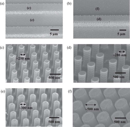
Figure 5 further shows that the nanopillar structures patterned on both the top and the bottom surfaces of the microgratings (period: ∼20 μm, height: ∼2 μm in figure 5(a); period: ∼65 μm, height ∼4 μm in figure 5(b)) using the tri-layer nanostencil membrane (nanopore pattern periodicity: ∼580 nm, pore diameter: ∼250 nm in figure 5(a); nanopore periodicity: ∼680 nm, pore diameter: ∼280 nm in figure 5(b)), following the schematic shown in figure 1(c). By depositing Cr nanodots through the nanostencil membrane on both the top and bottom surfaces of the micrograted silicon surface with no etch mask layers (e.g., PR or Cr) on either surface (figure 1(c-iv)) and then applying the DRIE on both surfaces, the nanopillar structures were formed on both the top and the bottom surfaces. It should be noted that the size (diameter) of the nanopillar created on the bottom surfaces of the shorter microgratings (figure 5(a)) was greater than that on the top surfaces by ∼20% (an increase from ∼250 to ∼300 nm). In contrast, the size of the nanopillar created on the bottom surfaces of the taller microgratings (figure 5(b)) was greater than that on the top surfaces by ∼78% (an increase from ∼280 to ∼500 nm). The increase of the feature size of the nanopillars with the height of the microstructures (or the depth of microtrenches) is due to the 'blurring' effect [21]. As discussed earlier (figures 4(a) and (b)), the Cr nanodots have a larger size on the bottom surfaces than on the top surfaces because of the 'blurring' effect. Thus the size (diameter) of the nanopillar structures patterned on the bottom surface is larger than that on the top surface. The 'blurring' effect becomes more pronounced as the height of the micrograting structure increases.
Figure 5. (a), (b) SEM images of the micrograted silicon surfaces (micrograting heights of 2 and 4 μm, respectively) whose top and bottom surfaces are both hierarchically patterned with nanopillar structures. (c), (d) Higher-magnification SEM images of the nanopillars patterned on the top (ridge) surfaces for the microgratings of 2 and 4 μm in height, respectively. (e), (f) Higher-magnification SEM images of the nanopillars patterned on the bottom (trench) surfaces for the microgratings of 2 and 4 μm in height, respectively.
Download figure:
Standard image High-resolution image
The maximum patterning depth on the microstructures with a clear definition of the nanostructures against the 'blurring' effect should be determined by several factors including the deposition source size and distance to the substrate, the feature size of the nanopatterns in the nanostencil, and the distance from the nanostencil to the substrate. As discussed earlier, the 'blurring' effect can be significantly reduced by either decreasing the feature size of the nanopatterns in the nanostencil or decreasing the gap distance between the nanostencil and the substrate with a given dimension of the deposition source size and distance to the substrate [23]. Meanwhile, in this study, only a 20 nm thick Cr layer was deposited through the nanostencil. Thus, we observed limited 'clogging' effects on the sidewalls of the nanopores in the nanostencil and the changes of the feature size. However, the 'clogging' effect could affect the patterning resolution with a thick metal deposition on the sidewalls of the nanopores. Then, a cleaning process could be used to reduce the 'clogging' effect [33]. With such a cleaning process, the soft nanostencil membrane can be reused as many as 5 times before mechanical failure. It should also be noted that it is possible to fabricate nanostencils with arbitrary features by using other nanopatterning techniques such as nanoimprint lithography or electron beam lithography followed by the nanostencil release and transfer protocols employed in this work, where only the periodic pore patterns were tested in this study using the laser interference lithography. Meanwhile, the height of the nanostructures is controllable in the DRIE step. Thus, the soft nanostencil lithography introduced in this work can accurately control the shape and size of the nanostructures on the microstructures in general.
5. Conclusion
In this study, we have successfully demonstrated that hierarchical nanostructures can be conveniently created on microstructures by using the soft nanostencil lithography technique. By simple modification of the fabrication processes and steps, we have shown that the hierarchical nanostructures can be selectively created only on the top or the bottom surfaces of the microstructures, or even for both surfaces, which is hard to be achieved by other top-down or bottom-up approaches. The soft nanostencil lithography technique demonstrated in this study has further advantages. The interference lithography technique employed in the preparation of the soft nanostencil is a low-cost and scalable method with the precise controllability of the pattern periodicity and feature size. The soft nanostencil membrane can be reused several times before mechanical failure, which significantly improves the efficiency of the nanostencil lithography. The multiscale hierarchical nanostructures that can be selectively defined on the surfaces of microstructures will open new doors to many applications such as biomedical diagnosis, energy harvesting, and nano-optics [34–37].
Acknowledgments
This study was supported by the Stevens Innovation & Entrepreneurship Doctoral Fellowship program and the US National Science Foundation (Award Number 1462499). This research was carried out in part at the Center for Functional Nanomaterials, Brookhaven National Laboratory, which was supported by the US Department of Energy, Office of Basic Energy Sciences, under contract No. DE-AC02-98CH10886. The research effort also used microscope resources partially funded by the ONR Defense University Research Instrumentation Program (Award No.: N00014-11-1-0841).