

Abstract
Despite the strong interest in optoelectronic devices working in the deep ultraviolet range, no suitable low cost, large-area, high-quality AlN substrates have been available up to now. The aim of this work is the selective area growth of AlN nanocolumns by plasma assisted molecular beam epitaxy on polar (0001) and semi-polar (11–22) GaN/sapphire templates. The resulting AlN nanocolumns are vertically oriented with semi-polar {1–103} top facets when grown on (0001) GaN/sapphire, or oriented at 58° from the template normal and exposing {1–100} non-polar top facets when growing on (11–22) GaN/sapphire, in both cases reaching filling factors ≥80%. In these kinds of arrays each nanostructure could function as a building block for an individual nano-device or, due to the large filling factor values, the overall array top surfaces could be seen as a quasi (semi-polar or non-polar) AlN pseudo-template.
Export citation and abstract BibTeX RIS
Introduction
AlN is a wide band-gap semiconductor (6.2 eV) particularly interesting for ultraviolet (UV) and deep UV (DUV) opto-electronics [1, 2] as well as micro/nano electromechanical systems [3]. Furthermore, AlN has been proposed as a building-block of high mobility transistors [4], field-emitters [5] and single-photon emitters [6].
For the particular case of UV LEDs, both planar multi-quantum well (MQW)-based devices as well as three-dimensional (3D) nanocolumn (NC)-based devices would have certain advantages and disadvantages. To date, the material growth and technology of planar MQW-based devices are more mature compared to their 3D counterparts. However, their efficiency, especially in the range between 200 nm to 280 nm, is seriously affected by: (i) a relative large threading dislocations density (TDD), larger than 108 cm−2 in AlN layers grown on standard substrates such as sapphire or SiC, (ii) a low light extraction efficiency (LEE), due to a strong polarization of the emitted light along the c-axis [7] as well as the light absorption of the p-type contacts or underlying planar substrate, and (iii) insufficient control of electrical properties (doping) [8, 9]. These issues might be solved by using NC-based devices [9], since AlN NCs are expected to benefit from advantages such as strain relief, improved crystalline quality, increased doping efficiency and a higher LEE compared to thin films, similar to other group(III)-N materials like (In,Ga)N.
So far, most of the work on Al(Ga)N NCs has focused on self-assembled (SA) arrays, either devoted to fundamental material studies [10–13], or to LED fabrication [9, 14]. The application of SA NCs in actual devices is strongly limited due to the wide spread of the structural (diameter, length, facets) and electrical properties. Recently, epitaxial growth of ordered homogeneous Al(Ga)N NCs arrays has been achieved, starting either by the etching down of an (Al,Ga)N layer (top-down approach) or the selective area growth (SAG) of GaN NCs (bottom-up approach), followed by AlN growth by metal-organic vapor phase epitaxy (MOVPE) [15, 16] or molecular beam epitaxy (MBE) [17, 18]. Besides homogeneous properties, these arrays would benefit from an additionally enhanced LEE by controlling the diameter and separation between NCs, as theoretical calculations have recently predicted [19].
This work reports on the SAG of AlN/GaN NCs on (0001) and (11–22) oriented GaN/sapphire templates, and their structural characterization by scanning electron microscopy (SEM), scanning transmission electron microscopy (STEM) and x-ray diffraction (XRD) to determine homogeneity, crystalline quality and strain state. Arrays of vertical or tilted AlN/GaN NCs are achieved depending on the starting GaN template orientation and as a consequence, a dense net of semi-polar {1–103} or non-polar {1–100} AlN top surfaces are formed.
Experimental details
The growth of AlN/GaN NCs was performed in a plasma-assisted MBE system on (0001) (sample A) and (11–22) (sample B)—oriented GaN/sapphire MOCVD templates. A 7 nm thick Ti film with nanoholes arranged in a triangular net, fabricated by colloidal lithography, was used for masking [20]. The diameter and pitch (distance between centers of adjacent holes) of the mask determine the dimensions and density of NCs grown (diameter: 170 nm, pitch: 280 nm).
First, the SAG of GaN nanostructures was accomplished under similar growth conditions as in previous works [21, 22]. Due to the relatively low diffusivity of Al ad-atoms in the presence of nitrogen (high energy Al–N bond), when trying the direct AlN SAG on the masked template, AlN spontaneously nucleates on the TiN mask instead of solely inside nano-holes (loss of selectivity). The GaN NCs grown first provide the means to avoid this parasitic nucleation by the shadowing effect, that is, by preventing the Al atoms to reach the TiN mask. A similar approach was successfully used before for InGaN NCs SAG [23].
The GaN NCs growth was performed at 860 °C, with a Ga-flux of 18 nm min−1 and an N-flux of 3 nm min−1. Following the GaN growth, AlN NCs were grown at 860 °C with an Al/N flux ratio close to stoichiometry, using impinging fluxes of around 2.4 × 10¹⁴ atoms/s cm2. The morphology and crystal structure of the samples was studied by SEM (FEI Inspect F) and STEM (FEI Tecnai F20). High-resolution XRD was performed with a PANalytical X´pert MRD diffractometer. A parabolic graded multilayer mirror collimator followed by a channel-cut four-bounce Ge(220) monochromator were set on the primary side. To assess the quality of the samples, rocking curves (RCs) and reciprocal space maps (RSMs) were collected with an open detector and 1 degree slit, respectively.
Results and discussion
Figure 1 shows top-view SEM pictures of the SAG GaN and subsequent AlN/GaN NCs grown on (0001) polar and (11–22) semi-polar GaN templates.
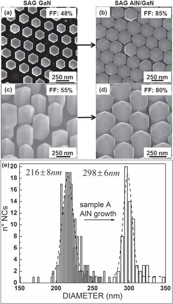
Figure 1. Top-view SEM pictures of (a) SAG GaN NCs grown on a (0001) GaN/sapphire template and (b) after AlN overgrowth (sample A); (c) SAG GaN NCs grown on a (11–22) GaN/sapphire template, and (d) after AlN overgrowth (sample B). The diameter distribution before and after the AlN growth in sample A is shown in (e).
Download figure:
Standard image High-resolution imageDepending on the GaN template orientation, the NCs are vertically aligned when grown on a (0001)GaN/sapphire template [21], or inclined when grown on a (11–22) GaN/sapphire semi-polar orientation [22]. In both cases the preferential growth direction is along the [0001] c-direction. GaN NCs length in sample A is about 450 nm, with lateral m-planes and an average diameter (corner-to-corner distance in the hexagonal section of the NCs) of 216 nm ± 8 nm, ending with pyramidal tops formed by 6 semi-polar {1–103} planes (figure 2(c)). GaN NCs in sample B are the same length (along c-direction), with diameters around 221 nm ± 6 nm and tilted 58° from the template normal, consistent with the angle between the (11–22) and the (0001) planes. In this case, most of the GaN NCs top surface (considering top surface as the surface mainly exposed to the molecular beams, hence the surface where growth mainly occurs) is formed by non-polar {1–100} m-planes (figure 2(d)). In addition to that, a smaller contribution of semi-polar {11–22} planes can be found.
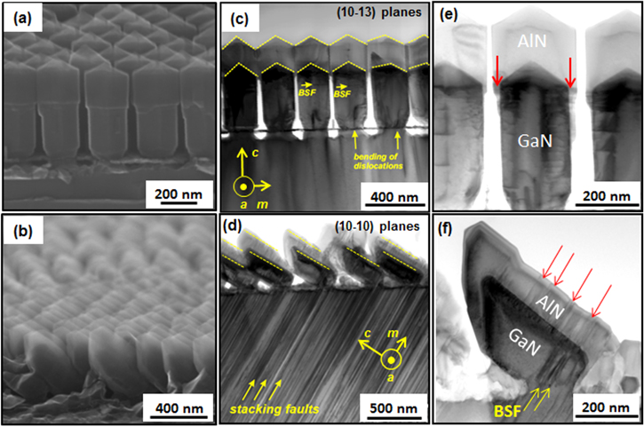
Figure 2. Bird's-eye view SEM pictures of (a) sample A and (b) sample B. In (c) and (d), cross-sectional STEM bright field images taken on samples A and B are shown, respectively. Dashed lines mark the main AlN/GaN interfaces and top surfaces. In (e) and (f) cross-sectional STEM bright field images of individual NCs of samples A and B are shown. The red arrows indicate the location of extended defects, found in the basal plane.
Download figure:
Standard image High-resolution imageTop-view SEM images of the samples after AlN overgrowth can be seen in figures 1(b) (sample A) and 1(d) (sample B). Comparing SEM pictures of the NCs before and after the AlN growth, a clear increase in NC diameter can be noticed (figures 1 and 2). In sample A the diameter increases from around 216 nm ± 8 nm to around 298 nm ± 6 nm upon AlN growth (figure 1(e)). This lateral growth leads to the formation of an AlN-shell/GaN-core structure observed at the interface region of each NC. AlN/GaN core–shell structures were reported before in SA (0001)-oriented NCs by MBE [11, 24–27]. In these SA structures the formation of the AlN shell was attributed to the lower diffusion of Al atoms compared to Ga atoms along the NCs sidewalls [12]. The same mechanism is assumed to drive the AlN shell formation in sample A. At this point it is worth noting that the radial growth in sample A seems to be limited under the given growth conditions and mask geometry in a way that the total coalescence of the NCs is avoided. A similar observation has been reported for the selective overgrowth of AlN on etched AlN pillars by MOVPE [15, 16] and on etched GaN pillars by MBE [17], both on (0001) oriented templates.
In sample B the situation is more complex due to the particular nanostructures geometry (not resembling a regular NC). Indeed, the NCs inclination exposes a large amount of the non-polar GaN facet to the impinging molecular beams, thus efficiently promoting the growth on them, as seen in figures 2(d) and (f).
The main top facets obtained after AlN growth are semi-polar {1–103} in the case of sample A and non-polar {1–100} for sample B, following the previously grown GaN. In the case of the SAG GaN on (0001) oriented templates, the top facets can be controlled by the local III/V ratio at the NCs nucleation stage [28], potentially allowing for the fabrication of AlN NCs with different semi-polar or even polar top facets on (0001) GaN/sapphire.
Due to the relatively small pitch of the SAG NCs and the lateral growth upon AlN growth, a large coverage of the substrate by the nanostructures is obtained in both samples, with filling factors (FF) reaching values ≥80%. Using dense arrays (large FF values) of homogeneous AlN nanostructures for further overgrowth combines the advantages of nanostructures' properties with an efficient use of the substrate, without the drawbacks of nanostructures' coalescence, as was pointed out in [15], where the AlN nanorods top facets consisted of a dense array of {1–101} planes, around 62° inclined with respect to the (0001) planes. Furthermore, the combination of large FF values with the semi-polar or non-polar character of the top facets is expected to be beneficial for opto-electronic devices (reduced polarization fields). In Al(Ga)N heterostructures the internal polarization field minimum value corresponds to non-polar orientations (or close to, depending on the Al content), while for In(Ga)N heterostructures minimum values exist for non-polar as well as semi-polar (around 45° with respect to the [0001] direction) orientations [29, 30]. Then, the top facets in sample A would reduce the polarization field in both (Al, Ga)N/GaN and (In, Ga)N/GaN heterostructures and moreover, across the {1–100} non-polar top facets in sample B, the polarization field would vanish for both types of heterostructures.
Bright field STEM measurements of samples A and B are shown in figures 2(c)–(f). In sample A, a high crystalline quality of the AlN sections grown on the semi-polar GaN planes is found (free of extended defects) since dislocations originating from the template are effectively bent taking advantage of the pyramidal top of the NCs (inclined facets) [31–33], and only few basal stacking faults (BSFs) are observed in the GaN section. In sample B, the high density of partial dislocations (and associated BSFs) present in the semi-polar GaN/sapphire template (density in the range of 107 cm−1) propagate only into the bottom part of the GaN nanostructures, being effectively filtered by the mask as well as by the void between neighboring overgrowing NCs [22] thus leaving most of the GaN volume free of defects. However, upon AlN growth on the non-polar {1–100} top facets new extended defects are generated (indicated by red arrows in figure 2(f)), with a density in the range of 105 cm−1 (two orders of magnitude lower than in the template). Also, some defects at the AlN/GaN interface indicate the formation of misfit dislocations. The formation of extended defects upon AlN growth on the non-polar facets can be observed as well in sample A (red arrows on figure 2(e)). A possible explanation for the additional defect formation could be the (anisotropic) tensile strain AlN is subjected to, being the thicknesses of GaN (core) and AlN (shell) above the critical values for coherent strain [34]. Moreover, it has been calculated that Al ad-atoms on (1–100) planes diffuse preferentially perpendicular to the [0001] direction [35], which agrees with the typical stripe-like morphology of m-plane AlN (nitrides) [36] and would be a backup for the formation of elongated features further coalescing with the subsequent defect creation.
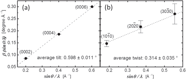
In order to confirm the overall crystalline quality and strain state of the entire ensemble of NCs, as an extension of the individual studies by STEM, sets of XRD measurements (spot size 1 mm × 10 mm) were performed on sample A. First, RSMs around symmetric and asymmetric reflections are taken and the AlN lattice parameters extracted. After that, tilt and twist values are extracted from Williamson–Hall plots, typically used for studying the tilt and twist between mosaic blocks in thin films, which relate to the density of screw type and edge type dislocations, respectively [37]. In the nanocolumnar case, tilt and twist values would relate to densities of out-of-plane and in-plane boundaries, not necessarily to dislocations, since the lateral m-planes of the NCs would be detected as boundaries as well. A more detailed study on the use of Williamson–Hall plots on the characterization of AlN NCs is going to be presented in a forthcoming paper. The same analysis cannot be performed on sample B, firstly because the dominant defects in semi-polar III-nitrides are BSFs, which have not been quantitatively studied by Williamson–Hall plots. Secondly, because of the crystalline orientation some planes do not allow for the scan configuration (limitations on the equipment movement) and additionally, the broadening of RCs of skew-symmetric scans relate to NCs tilt, twist and finite size, so the corresponding Williamson–Hall plots could not be used to describe either NCs tilt or twist.
Figure 3 shows RSMs around (0002) symmetric and (10–15) asymmetric AlN/GaN reflections for sample A. The (0002) RSM reveals a high quality AlN segment, without macroscopic tilts between the GaN and the AlN (the two peaks centered at Qx = 0). The small broadening of the (0002) RSM along the Qx direction (∼about 0.03 A−1) indicates low tilt values (and sufficiently large NCs). It can be seen from the (10–15) RSM that the diffraction from the AlN and GaN sections have different lattice positions, evidencing growth of relaxed AlN NCs. In order to estimate the AlN lattice parameters minimizing errors, (0002), (0004) and (0006) symmetric RSMs with different azimuth angles were collected, as well as asymmetric (10–15) and (10–14) RSMs. It was found that the c and a lattice parameters of AlN on sample A are 4.982 ± 0.004 Å and 3.11 ± 0.003 Å, respectively, which are close to values of strain-free AlN [38, 39].

Figure 3. Reciprocal space maps around the symmetric (0002) and asymmetric (10–15) AlN/GaN reflections from sample A.
Download figure:
Standard image High-resolution imageAfter that, Williamson–Hall plots were performed; the average tilt of AlN NCs was estimated from the RCs of (0002), (0004) and (0006) with different azimuth directions while the average twist angle was estimated from the RC of (10–10), (20–20) and (30–30) measured using the grazing incidence diffraction method. Figure 4 shows the respective plots for extracting AlN average tilt (figure 4(a)) and twist (figure 4(b)). Sample A shows a relatively small average tilt and twist angles, with values 0.598 ± 0.011° (average tilt) and 0.314 ± 0.035° (average twist), indicating low micro-strain related to dislocations or other boundaries in the NCs. There are no studies for the tilt and twist of AlN NCs, but we can compare very favorably the present values to the reported ones for SA GaN NCs, typically on silicon (values range from 1.4°–5°), where the coalescence of misoriented NCs is hard to be avoided [40, 41]. Here it is worth commenting that for SA GaN NCs grown on AlN/6H-SiC(000–1) the tilt and twist values are reduced compared to the silicon case, although the reported twist is still double the present case [41]. As for AlN layers grown on sapphire substrates, the tilt and twist values reported in literature depend on the growth technique; in general the present values are better than the ones for MBE AlN grown layers [42, 43], but lower numbers are found for improved MOCVD growth [44]. However, it has to be considered that in thin films the tilt and twist of mosaic blocks relate to the density of screw type and edge type dislocations [37], but not necessarily in the case of nanocolumnar samples; in the case of NCs, the lattice distortion caused by their finite size (lateral m-planes) can be responsible for part of the tilt and twist found here. The tilt and twist values measured in sample A correspond to a density of out-of-plane and in-plane boundaries of 10 ± 0.4 × 109 cm−2 and 7.1 ± 1.6 × 109 cm−2, respectively. Considering the finite size of the NCs, with six lateral m-planes acting as boundaries, and the NCs density (around 1.5 × 109 cm−2), XRD analysis indicates AlN on sample A can be considered free of edge dislocations and with a low density screw dislocation.
Figure 4. Williamson–Hall plots for extracting the average tilt (a) and average twist (b) of AlN in sample A.
Download figure:
Standard image High-resolution image
Conclusion
In this work the selective area growth of high quality AlN/GaN NCs on polar (0001) and semi-polar (11–22) GaN/sapphire templates with filling factors ≥80% was demonstrated. The AlN/GaN NCs grown on (0001) GaN/sapphire were found to have pyramidal tops formed by semi-polar {1–103} planes, where AlN top facets follow exactly the top facets of the previously grown GaN. When growing AlN/GaN NCs on (11–22) GaN/sapphire, the NCs were inclined 58° from the normal template making the non-polar m-planes the dominant top surfaces. In these kinds of arrays, a dense net of semi-polar {1–103} (sample A) or non-polar {1–100} (sample B) AlN top surfaces were formed with a very high crystalline quality in the case of sample A, and the formation of extended defects in the case of sample B. However, the defect density in the non-polar plane of AlN in sample B is around two orders of magnitude lower than in the semi-polar GaN template. The high crystalline quality and the fact that the top facets would reduce or remove the polarization fields in both (Al,Ga)N/GaN and (In,Ga)N/GaN heterostructures, make these kinds of nanostructures appealing building blocks, or pseudo-templates, for emitters and detectors working in the deep-UV and UV range whose efficiency nowadays is limited by the quality of the available material.
Acknowledgments
We acknowledge partial financial support from Spanish project MAT2015-65120-R. M–Y Xie thanks the European Union's Horizon 2020 research and innovation programme under the Marie Skłodowska-Curie grant agreement no. 658349. We also thank the German Research Foundation DFG for financial support within the major research program INST272/148-1 and the Collaborative Research Center SFB787, 'Semiconductor Nanophotonics: Materials, Models, Devices'.