

Abstract
The influence of water vapor on the electronic property of MoS2 field effect transistors (FETs) is studied through controlled experiments. We fabricate supported and suspended FETs on the same piece of MoS2 to figure out the role of SiO2 substrate on the water sensing property of MoS2. The two kinds of devices show similar response to water vapor and to different treatments, such as pumping in the vacuum, annealing at 500 K and current annealing, indicating the substrate does not play an important role in the MoS2 water sensor. Water adsorption is found to decrease the carrier mobility probably through introducing a scattering center on the surface of MoS2. The threshold voltage and subthreshold swing of the FETs do not change obviously after introducing water vapor, indicating there is no obvious doping and trap introducing effects. Long time pumping in a high vacuum and 500 K annealing show negligible effects on removing the water adsorption on the devices. Current annealing at high source-drain bias is found to be able to remove the water adsorption and set the FETs to their initial states. The mechanism is proposed to be through the hot carriers at high bias.
Export citation and abstract BibTeX RIS
1. Introduction
Molybdenum disulfide (MoS2) has attracted much attention as a novel two-dimensional (2D) material for electronics [1–4], optoelectronics [5–8], valleytronics [9–14], transparent and flexible devices [15–18], and sensors [19, 20]. One limitation of MoS2-based devices is their high sensitivity to extrinsic effects, such as environmental gases, which cause the instability of the device properties [19–22]. The influence of water vapor on MoS2 is not yet clear. Some works suggest water vapor is an electron acceptor [23], which increases the resistance of the MoS2 device. While some other evidence show water vapor causes hysteresis behavior in field effect transistors (FETs) [24], but the depletion of the electron is not so obvious [21, 24]. On the other hand, the desorption of water molecules from MoS2 is difficult compared with other gases [21, 25]. Furthermore, the mechanics of the above phenomena has not been studied well. Besides the channel materials, substrate is an important factor for the electronic performance of 2D materials devices. It has been confirmed that water adsorption on SiO2 substrate has a negative influence on the performance of graphene devices [26, 27]. However, similar study on MoS2 devices is rare.
In the present study, we investigate the effect of water on the electronic properties of MoS2 FETs and the way to remove the water adsorption and recover the device property.
2. Experimental
The exfoliated MoS2 sheets were transferred onto 300 nm-thick SiO2 covering a highly doped p++ Si wafer as a back gate. Two FETs, supported and suspended, were fabricated on the same piece of MoS2 with the same channel length and width. The source and drain electrodes were patterned using electron beam lithography (EBL), followed by the deposition of Cr/Au 5 nm/70 nm using electron beam evaporation (EBE). Then, a window was defined by EBL on the channel of one of the two neighboring devices on the same piece of MoS2, and the SiO2 beneath the channel was etched away with buffered HF solution. After the cleaning process, the sample was moved out from hot isopropanol with low surface tension to make the MoS2 channel suspended. A schematic diagram and a scanning electron microscope (SEM) image of a couple of FETs are shown in figure 1. The optical images and Raman spectrum of the MoS2 are given in online supplementary information. The electronic characteristics of the devices were measured using a semiconductor characterization system (Keithley, 4200) in a probe station (Janis, ST500) that allows for controlling the environment in the sample chamber and in situ annealing. We fabricated several devices through the same process and obtained similar results. The water we used is ultrapure water with its resistivity being 18 MΩ · cm, and the water vapor pressure is 2.33 KPa after water vapor is introduced into the sample chamber.
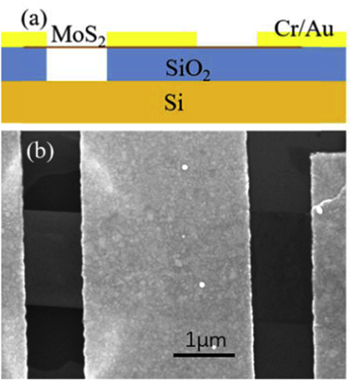
Figure 1. (a) and (b) A schematic diagram and a SEM image of a pair of FETs with one suspended device and one supported device fabricated on the same piece of MoS2 sheet.
Download figure:
Standard image High-resolution image3. Results and discussion
First, the transfer curves and output curves of the FETs based on a 3 layer MoS2 (The optical images and Raman spectrum of the MoS2 are given in online supplementary information) were measured in the vacuum with the pressure of 3.3 × 10⁻³ Pa, the results are shown in figure 1 as black lines. The threshold voltage of the suspended FET is negative, while that of the supported FET is near 0 V, indicating that the SiO2 substrate can deplete electrons from the MoS2 channel and decrease the carrier concentration. The subthreshold swing (SS) of the supported device is worse than that of the suspended device due to the impurities between the substrate and MoS2 sheets [28, 29].
After introducing water vapor into the sample chamber, the transfer curves and output curves of the FETs were measured again, the results are shown in figure 2 as red lines. The suspended and supported devices display a similar response to water vapor, the on-state current drops to about 40% of the original value, but the threshold voltage and SS do not change obviously. Water adsorption on SiO2 has been reported to have a strong effect on nanomaterials devices, such as graphene [26, 27]. However, here, the suspended and supported MoS2 devices fabricated on the same piece of MoS2 have the same response to water. Therefore, it should be the water adsorption on the MoS2 itself that affects the electronic properties of the FETs, the effect of SiO2 is not important. The fact that SS does not change before and after water introduction indicates water does not introduce interface trapping which can change the gate efficiency. The threshold voltage does not change obviously, together with the unchanged SS, indicates the carrier density does not change obviously before and after introducing water vapor. Therefore, the decrease of the on-state current is mainly due to the decrease of the transconductance and mobility.
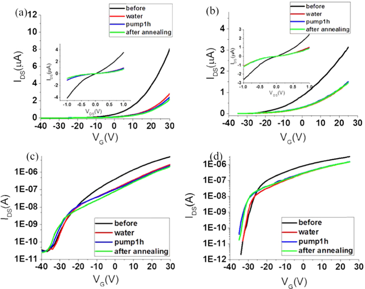
Figure 2. (a) and (c) show the transfer curves of a supported device, (b) and (d) show those of the suspended device coupled with the supported device in (a) and (c). All the measurements were made at VDS = 1 V. (a) and (b) are in linear coordinates, while (c) and (d) are in logarithmic coordinates. The inset of (a) and (b) are the corresponding output curves of the devices measured when VG = 20 V. We made the measurements as follows: measure the transfer curves in the vacuum first (labeled by 'before'), then measure in water vapor (labeled by 'water'), measure after 1 h pumping and the pressure in the sample chamber returned to the vacuum (labeled by 'pump 1 h'), measure after annealing at 500 K and then cooling down to room temperature (labeled by 'after annealing').
Download figure:
Standard image High-resolution imageIn order to remove the water adsorption, we pumped the sample chamber for an hour. When the pressure in the chamber was around 3.3 × 10⁻³ Pa, we measured the electronic characteristics again. As shown by the blue lines in figure 2, the electronic characteristics after pumping are about the same as that in water vapor for both the supported and suspended FETs. This result indicates pumping in the vacuum cannot remove the water adsorption.
Then we heated the sample to 500 K in the vacuum trying to remove water adsorption by heat. After annealing for about 1 h, the sample was cooled down to room temperature in the vacuum, and we measured the electronic property of the devices again. As shown in figure 2 as green lines, the electronic characteristics after annealing are about the same as that in water vapor for both the supported and suspended FETs. This result indicates thermal annealing in vacuum cannot remove the water adsorption on the MoS2, either.
In order to confirm the above results, we repeated the experiments again on the same devices. This time, we pumped the sample in the vacuum (3.3 × 10⁻³ Pa) for 12 h. After the long pumping time, the transfer curves still have very little change in the linear coordinates, while in the logarithmic coordinates, a threshold shift to the negative side can be observed in both the suspended and supported FETs, as shown in figure 3. This threshold shift can be attributed to the desorption of oxygen induced by long time keeping in a high vacuum, as has been reported previously [30]. Besides the threshold shift, no other difference is observed from the electronic properties after the two pumping processes. These results confirm that pumping in vacuum cannot remove the adsorbed water on MoS2.
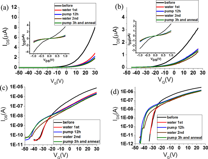
Figure 3. (a) and (c) show the transfer curves of a supported device, (b) and (d) show that of the suspended device coupled with the device in (a) and (c). All the measurements were made at VDS = 1 V. (a) and (b) are in linear coordinates, (c) and (d) are in logarithmic coordinates. The inset of (a) and (b) are the corresponding output curves of the device measured when VG = 20 V. We made the measurement as follows: measure the transfer curves in vacuum first (labeled as 'before'), measure in water vapor for the first time (labeled as 'water 1st'), measure after 12 h pumping in vacuum (labeled as 'pump 12 h'), measure in water vapor introduced for the second time (labeled as 'water 2nd'), then anneal at 500 K, cool down to room temperature, pump the sample chamber for 3 h, and then make the measurement (labeled as 'pump3 h and anneal').
Download figure:
Standard image High-resolution imageAfter the long pumping time, we introduced water vapor into the sample chamber again and measured the electronic characteristics. As shown in figure 3, the transfer curves obtained in water vapor for the first and the second times are about the same, which means the effect of water gas adsorption has been maintained from the first time to the second time. This can be explained as followed: the adsorption positions have been occupied in the first time water vapor introducing, not much more water molecules can be absorbed to the MoS2 surface further in the second time, so that the electronic properties remain roughly the same.
The sample chamber was then pumped back to the high vacuum and the devices were annealed at 500 K again. The electronic characteristics measured after the pumping and annealing process are shown in figure 3 as green lines, the results are similar to that shown in figure 2. The above observation proves that the water molecules adsorbed on the MoS2 sheets are difficult to remove simply by pumping in vacuum and/or thermal annealing in vacuum.
We would like to emphasize here that the response to the water vapor and the different treatments performed here are the same for both the suspended FETs and the supported FETs, so that the SiO2 substrate and its interface with the MoS2 channel do not play an important role on the water sensing property of MoS2 devices. As mentioned above, the on-state current decrease in water vapor is mainly due to the decrease of the transconductance and mobility. Since the same samples are compared before and after water adsorption, the channel length L, the channel width W, the capacity of the insulator Ci and the source-drain voltage VDS are fixed, the variation of transconductance can be fully explained by the variation of carrier mobility. The carrier mobility can be calculated by  where W = 2 μm and L = 1 μm in the present devices, VDS = 1 V and Ci is the capacity per unit area of 300 nm thick SiO2/vacuum insulate layer. The mobility of the suspended devices is found to drop from 18.2 cm2 (V · s)−1 to 10.6 cm2 (V · s)−1 after water adsorption and the mobility of the supported devices drops from 17.1 cm2 (V · s)−1 to 7.3 cm2 (V · s)−1 after water adsorption.
The carrier mobility obtained above is field effect mobility, which is also affected by the contact resistance. To evaluate the possible influence of the contact, we measure the contact resistance of the devices with the transfer length method. Supported devices with different channel length (0.5 μm, 1 μm, 1.5 μm) were fabricated on the same piece of a 4 layer MoS2 sheet (The Raman spectrum and the optical images are given in the online supplementary information), as shown in figure 4. The source and drain metal and their fabrication method are the same as the above suspended and supported FETs. As shown in figure 5, the devices with difference channel length have the same threshold voltage before and after water adsorption. The contact resistance is the half of the y intercept of the resistance versus channel length plots at Vg = 20 V (at the on-state). The contact resistance is 8.8 KΩ in the vacuum and 12.0 KΩ in water vapor, while the total resistance is 118 KΩ and 297 KΩ for the 0.5 μm device, as shown in figure 5(c). The total resistance of the devices with longer channels are higher than that in the 0.5 μm device. To take the contact resistance into account, the current should be  where Rc is the total contact resistance and Rch is the resistance of the channel. Therefore, the modified mobility should be multiplied by a coefficient
  Due to the small contact resistance relative to the channel resistance, the modified mobility is around 22 cm2/(V · s) before water adsorption. Note, even the modified mobility is still lower than the high value in the literature [31]. The decrease of field effect mobility after water adsorption indicates the decrease of carrier mobility in the channel. As the suspended devices have similar responses as the supported devices to water vapor and the different treatments, the above statement is also true for the suspended devices. The mechanism should be that the adsorbed water molecules form new scattering centers on the MoS2 surface, which reduces the carrier mobility. The slightly increased mobility of the suspended devices can be explained by the removal of the substrate. We observed many Coulomb impurities in the interface between SiO2 substrate and MoS2, which induce relative low mobility [32]. Because the fabrication processes of the present devices include wet etching, impurities and defects could exist after etching, a very clean and perfect surface is difficult to achieve. This could explain why the mobility in the suspended devices before water adsorption is still not the highest compared with that in the literature.
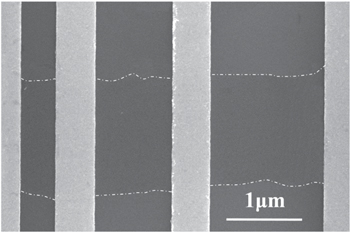
Figure 4. The SEM image of the MoS2 devices with different channel lengths: 0.5 μm, 1 μm and 1.5 μm. The dashed lines indicate the edge of the MoS2 sheet.
Download figure:
Standard image High-resolution image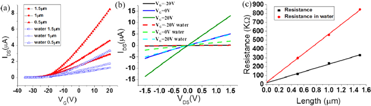
Figure 5. (a) The transfer curves of the devices with different channel length on the same pieces of MoS2. The red points are measured in the vacuum, and the blue points are measured in water vapor. (b) The output curves of a 0.5 μm channel length device at different gate voltage. The solid lines are measured in the vacuum, the dashed lines are measured in water vapor. (c) The resistance of the devices with different channel lengthes at VG = 20 V.
Download figure:
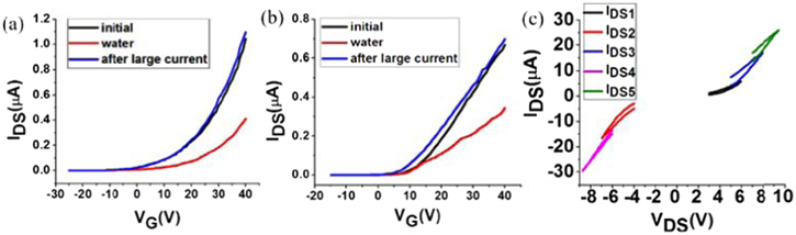
Standard image High-resolution imageThen, is there any way to remove the water adsorption and recover the electronic property of MoS2 FETs? We have found a method here. As shown in figure 6, the transfer curve returns to the initial state after a large current passing through the device. We fix the gate voltage at 30 V to set the device to the on-state, and we increase the drain voltage gradually, as shown in figure 6(c). First, we set the drain voltage VDS to change from 3 V to 6 V, and then back to 3 V, and measure the curve IDS1 shown in figure 6(c). Next, we set VDS to change from −4 V to −7 V, and then back to −4 V, and obtain the curve IDS2. The curves, IDS3, IDS4 and IDS5, are obtained when VDS changes at higher levels step by step. In this process, the current in the MoS2 channel increases step by step. The water adsorption can be removed when a large current passes through the MoS2 channel for both the supported and the suspended devices. As described in detail in our recent work [33], we can estimate the temperature distribution for VDS = 5 V and IDS = 100 μA through Comsol by taking into account all the factors, including the Joule heat, the thermal conductivity and the thermal capacity of the MoS2, SiO2, Si substrate and the metal electrodes, etc. We find the temperature increased by Joule heating at the present current is less than 447 K for the supported devices, which is less than the temperature in the heat annealing process. Therefore, the increase of the on-state current cannot be attribute to heat annealing.
Figure 6. (a) The transfer curves of a supported device at VDS = 1 V. (b) The transfer curves of the suspended device coupled with the device in (a) at VDS = 1 V. (c) I-V curves during the current annealing. The black curves labeled by 'initial' in (a) and (b) were measured in the vacuum before introducing water vapor and any treatment. The red curves labeled by 'water' in (a) and (b) were in water vapor. The blue curves labeled by 'after large current' in (a) and (b) were measured after pumping the sample chamber back to high vacuum and performing current annealing.
Download figure:
Standard image High-resolution image
The adsorption energy of water on MoS2 has been found to be around 0.2 ∼ 0.3 eV according to previous computation results [34, 35]. The phonon energy is around 0.026 eV at room temperature, and around 0.05 eV at 500 K (the present thermal annealing temperature), these energies are much less than the adsorption energy. Therefore, it is understandable that pumping in the vacuum and thermal annealing cannot remove the water adsorption from MoS2. Why can current annealing remove the water adsorption and recover the property of MoS2 FETs? We propose the following explanation. The contact between Cr/Au and MoS2 has a Schottky barrier. At large VDS, the electrons inject into the conduction band of the MoS2 channel should experience a strong band bending at the MoS2-metal contact, which could generate excitons via impact excitation [36]. The energy distribution of those hot carriers no longer obeys Boltzman distribution under a high electric field [37]. The hot carriers have been found to induce gas desorption in semiconductors [38, 39] and metals [40]. As the source-drain bias we applied is similar to that in [36], the hot electron energy in this work should be similar to that in [36], where hot carrier associated excitons have been demonstrated. The energy of the hot carriers (electrons) is sufficient to generate excitons and is larger than the desorption energy of water from MoS2, so that can cause water desorption.
4. Conclusions
The effects of water on MoS2 FETs and their recovery are studied. The suspended and supported MoS2 devices fabricated on the same piece of MoS2 show similar response to water and to different treatments (such as pumping in vacuum, thermal annealing and current annealing), indicating the effects of the SiO2 substrate and its interface with MoS2 are negligable. Water adsorption is found to decrease the mobility of MoS2 probably through introducing a scattering center on the surface. Water vapor is found not to introduce doping or traps obviously, demonstrated by the unchanged threshold voltage and SS after water adsorption. Long time pumping in the vacuum and thermal annealing in the vacuum cannot desorb the water molecules. We find current annealing at high source-drain bias can effectively remove the water adsorption and recover the electronic property of the MoS2 FETs, and we propose the mechanism is through the high energy hot carriers under large bias.
Acknowledgments
We thank Yuxiang Han, Zhiqiang Tang, Mei Sun and Xing Li for valuable discussions. This work was supported by the NSF of China (No. 11374022, 11528407 and 61621061).