
Abstract
Magnonics is a budding research field in nanomagnetism and nanoscience that addresses the use of spin waves (magnons) to transmit, store, and process information. The rapid advancements of this field during last one decade in terms of upsurge in research papers, review articles, citations, proposals of devices as well as introduction of new sub-topics prompted us to present the first roadmap on magnonics. This is a collection of 22 sections written by leading experts in this field who review and discuss the current status besides presenting their vision of future perspectives. Today, the principal challenges in applied magnonics are the excitation of sub-100 nm wavelength magnons, their manipulation on the nanoscale and the creation of sub-micrometre devices using low-Gilbert damping magnetic materials and its interconnections to standard electronics. To this end, magnonics offers lower energy consumption, easier integrability and compatibility with CMOS structure, reprogrammability, shorter wavelength, smaller device features, anisotropic properties, negative group velocity, non-reciprocity and efficient tunability by various external stimuli to name a few. Hence, despite being a young research field, magnonics has come a long way since its early inception. This roadmap asserts a milestone for future emerging research directions in magnonics, and hopefully, it will inspire a series of exciting new articles on the same topic in the coming years.
Export citation and abstract BibTeX RIS

Original content from this work may be used under the terms of the Creative Commons Attribution 4.0 licence. Any further distribution of this work must maintain attribution to the author(s) and the title of the work, journal citation and DOI.
This article was updated on 18 August 2021 to correct the name of an author, affiliations, permissions statements in figures and minor typographical errors.
Introduction
Anjan Barman1 and Gianluca Gubbiotti2
1S N Bose National Centre for Basic Sciences, India
2Istituto Officina dei Materiali del Consiglio Nazionale delle Ricerche (IOM-CNR), Italy
The concept of spin waves was first introduced by F Bloch in 1932 [1] and further developed by Holstein & Primakoff [2] and Dyson [3] who laid the foundation of spin waves theory. Although effects of periodic modulation on wave propagation was known since the late 19th century, and concept of pass and stop bands was introduced for electromagnetic wave propagation in 1950s [4], it was introduced in the magnetic system after two decades [5]. Subsequently, different kinds of periodic modulation have been introduced. However, the invention of photonic crystal [6] has fueled intense interest in spin waves in periodic magnetic media in the late 1990s [7] and a new field named magnonics was born. In 2001, the term magnonic crystal (MC) was coined by Gulyaev and Nikitov [8] and later by Puszkarski and Krawczyk as the magnetic counterpart of photonic crystals [9].
Magnonics deals with the excitation, propagation, control and detection of spin waves (quanta of which are called magnons) through periodic magnetic media consisting of either passively (patterned structures, modulated magnetic properties) or actively (spin texture, electric field, magnetic field) controlled modulation. It is analogous to photonics or phononics but it has several advantages over its photonic or phononic counterparts. These include lower energy consumption, easier integrability and compatibility with complementary metal-oxide semiconductor (CMOS) structure, programmability, shorter wavelength, smaller device features, anisotropic properties, negative group velocity, non-reciprocity and efficient tunability by various external stimuli to name a few. Hence, despite being a young research field, magnonics has come a long way since its early inception. A flurry of research on propagating and confined spin waves have unraveled a plethora of fundamental physics, and a handful of prototype devices and concepts such as magnonic memory, logic, transistor, transducers, RF components (filters, diodes and circulators), all-magnon circuits and neuromorphic computing have been unearthed. This brings us to the important milestone of preparing a roadmap of magnonics research in the coming years.
This is the first roadmap on magnonics. Three roadmaps of magnetism have already been published by IOP in 2014, 2017 and 2020, where few aspects of magnonics and spin dynamics have been discussed. However, a comprehensive roadmap solely dedicated to magnonics has been long due. Magnonics community organize the international workshop titled 'Magnonics: From Fundamentals to Applications', every two years which has become a benchmark conference not only for the magnonics community but also for researchers working in related fields like spintronics, microwave electronics, nanomagnetism, etc. In addition, an 'International Advanced School on Magnonics' is organized every two years. Further, Magnonics sessions regularly feature at the major international conferences (e.g. MMM, Intermag, JEMS, APS meetings, etc). The number of research papers and citations in this field has steadily increased over last three decades and experienced huge upsurge during the last one decade. Hence, the time is ripe to prepare a roadmap on magnonics.
This roadmap aims to encompass the state of the art in the field of magnonics [10, 11] and to move forward in the quest for new concepts, phenomena and techniques for the ultimate goal of translational research in the coming years. We search for ways to conjugate the substantial knowledge-base made in the conventional and emerging topics of magnonics (e.g. spin textures, strong coupling, topology, biology, spin–orbit effects) and lead toward hybrid magnonics, where more than one effects/stimuli can drive each other or have interconversion for discovering novel phenomena, as well as developing more robust and efficient devices (figure 1). The roadmap is an interdisciplinary collection of sections written by leading experts in the field where classical magnonics merges with quantum effects, e.g. spin–orbit coupling (SOC), the spin Hall and spin pumping effect, Dzyaloshinskii–Moriya interaction (DMI), superconductivity, nonlinearity, topology, etc.
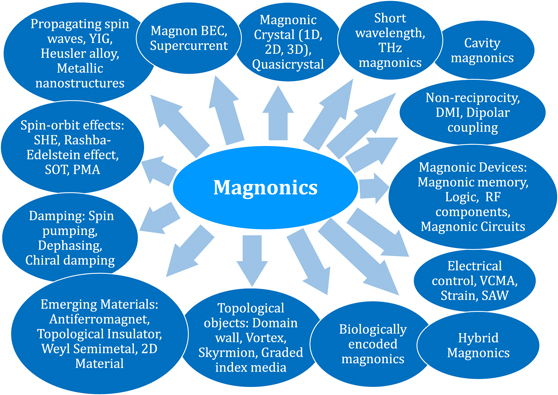
Figure 1. The many branches of magnonics.
Download figure:
Standard image High-resolution imageThe roadmap contains a discussion of fabrication techniques of planar and three-dimensional magnonic structures using top-down and bottom-up approaches besides patterning of spin textures (section 1). The research on planar MC have matured substantially during the last one decade and the future challenges lie in extensive research in unconventional structures, quasi-periodic lattices, controllable modulators, vortex and skymion lattices, etc (section 2). Efforts on the extension of planar MC toward the third dimensions has just started [12], which promises very complex spin-wave dispersion and confinement effects (sections 1, 2 and 6). The 3rd dimension can be exploited to control the in-plane propagation of spin waves, offering a robust route for designing non-reciprocal magnonic spectra with chiral properties without the need for DMI and sophisticated material growth. 3D integrations with respect to 2D systems permit to fit more functionality into a smaller space, allowing a large number of vertical connections between the layers, and an increase of the density of elements for the fabrication of scalable and configurable magnonic networks. Moreover, curved surfaces and 3D micro- and nano-objects exhibit peculiar and unexpected spin textures which are normally not observed in planar nanostructures and allows for the exploitation of magnon's chirality and the resulting non-reciprocity of the magnon dispersion (section 6). One of the most fundamental topics of magnonics is magnon Bose–Einstein condensation (BEC). Beyond conventional parametric pumping, kinetic instability regime, rapid cooling, spin pumping effect have been explored to attain more efficient magnon-BEC. On the other hand, various indirect confirmation of magnon supercurrent, which is considered to be a key element of information transfer from magnon-BEC, has been obtained, e.g. by observation of quantized vortices in a two-component Bose–Einstein condensate by using Brillouin light scattering (BLS) spectroscopy (section 5).
A very important aspect of modern magnonics is to use exchange-dominated short-wavelength magnons as it promises high-speed magnonic devices and data processing. However, conventional microwave antenna-based excitation is inefficient and new approaches such as resonant and non-resonant magnonic nanogratings, ferromagnetic coplanar waveguides (CPWs), parametric pumping, spin-transfer torque and spin textures will be useful. Some important issues like using topologically protected magnetic states as nanochannels of low damping and magnon-qubit coupling scheme involving short-wavelength magnons for integrated hybrid quantum systems have been discussed in section 7. Optically inspired magnonics, based on spin-wave nano-optics and easy local modification of 'optical' properties can be useful for miniaturization of devices using short-wavelength magnons in metallic ferromagnets, but high damping and low dynamic range limit the maximum achievable device size (section 9). Anti-damping torque from the spin–orbit effect can play a crucial role in damping modulation (sections 10 and 13) [13]. Voltage-controlled magnonics can offer energy-efficient alternatives in beyond-CMOS computing and a two-pronged approach can be taken to this end, using magnon straintronics (section 8) and voltage-controlled magnetic anisotropy (VCMA, section 18). While the former depends on inverse magnetostriction (Villari effect), the latter works on the change in electronic occupation at the ferromagnet/oxide interface and the ensuing orbital hybridization. Both the effects can excite and control spin waves and produce dynamic MC and magnonic nanochannels. SOC effects can play a big role in energy-efficient magnonics, and effects like perpendicular magnetic anisotropy (PMA), spin Hall effect (SHE), Rashba effect, spin pumping, spin caloric effect and DMI have already been extensively used in various branches of magnonics ranging from magnon-BEC to magnonic devices. They have their origin both in the intrinsic and extrinsic mechanism, where the latter can be efficiently engineered to externally control magnonic systems made of SOC materials. The SHE can cause auto-oscillation by completely compensating damping and this auto-oscillation in a nano-notch SHE oscillator have shown to efficiently emit unidirectional propagating spin waves into a magnonic waveguide. The propagation length of emitted spin waves has been enhanced by up to a factor of three by the spin current injected over the entire length of the waveguide. However, nonlinear scattering of propagating spin waves from magnetic fluctuations and spatial self-localization of oscillations, preventing the emission of propagating spin waves both caused by the pure spin current are important issues to be addressed in future (section 10).
Spin wave non-reciprocity is both fundamentally and technologically important and it occurs when spin-wave propagation changes or becomes forbidden upon inversion of the propagation direction and requires a breaking of the time-reversal symmetry (section 16). Various effects such as surface acoustic wave (SAW), dipolar interaction, gradient magnetic field and interfacial DMI (iDMI) can give rise to such non-reciprocity. Such non-reciprocal propagation can continuously tune the magnonic band structure and bandgap in MC with iDMI (section 13). The introduction of periodic DMI can cause indirect magnonic gaps, flat bands and complex temporal evolution of the spin waves, and can be regarded as a chiral MC, where topological magnons should be observed (section 16). iDMI also plays important role in stabilizing chiral spin textures, which can affect the magnon propagation giving rise to the topological and magnon Hall effect. Spin textures play a key role in magnonics due to their stability and resilience combined with a remarkable degree of tunability and scalability toward nanoscale dimensions. Some prominent examples are spin-wave channelling within domain walls, reconfigurable MC and reprogrammable spin-wave circuits (section 11). A related field is the graded-index magnonics where tailored graded magnonic landscapes from nonuniformity of internal magnetic field can be exploited to create practical devices such as magnonic Luneburg lens. However, development of designer magnonic landscapes with low damping is a major challenge ahead (section 12). Antiferromagnetic and THz magnonics offer ultra-high frequency devices. In antiferromagnets, the THz eigenfrequency stems from the very high sublattice exchange field, while laser-induced spin current in a ferromagnet/nonmagnet thin films can also cause THz spin-wave emission due to the confinement of exchange standing spin waves in nanometer-thick layer. Synthetic antiferromagnets (SyAFs) and angular momentum compensated ferrimagnets also exhibit exotic spin dynamics. Magnetic damping measurements and direct observation of antiferromagnetic magnon modes are crucial future challenges, while magnon current driven by all-electronic on-chip THz sources may enable novel energy-efficient spin memories operating at THz frequencies (sections 14 and 15). Spin-wave power flow and caustics will be important in magnonic computing which may require the creation of multiple spin-wave beams and methods to tune the focusing on a small and local scale. Magnon focusing can occur by playing with the curvature of the isofrequency curve, viz by tuning internal system parameters such as magnetic anisotropy, iDMI, nanostructuring or by external control such as electric field, magnetic field, spin-polarized current etc (section 17). Cavity magnonics is an emerging field that emphasizes strong coupling between cavity photons and magnons because of their coherence over large distances, whereas magnons and phonons also generate indirect interactions between tiny magnets over large distances. A coherent magnon–photon coupling causes photon-magnon mode repulsion. Some challenges in this field are to customize and load cavities, chiral interaction leading toward designing chiral magnonic molecules and increased nonlinearity for creating tripartite entanglement between magnons, photons and phonons (section 19).
Topologically protected magnon modes hold great promises due to their inherent robustness against defects and imperfections and their generic chirality, whereas possible applications in advanced and quantum information processing may occur due to lower dissipation and possible coherent control of magnons. However, their experimental confirmation is still limited to the magnon Hall effect and observation of topological magnon bands. To this end, one of the major challenges will be to find systems with strong DMI for the generation of a Berry curvature of the magnon bands leading toward a transverse deflection of the exchange dominated magnon current so that it can be detected at higher temperatures and occurred on shorter time scales (section 20). Superconductor/ferromagnet (S/F) hybrid systems at low temperatures offer highly interesting physics, e.g. spin-polarized triplet supercurrents via spin mixing and spin rotation processes in proximity coupled S/F interface and a fluxon-induced MC in proximity decoupled S/F bilayer system in out-of-plane magnetic fields, when the superconductor attains a mixed state having Abrikosov vortices. S/F heterostructures can also allow for highly efficient magnon–photon coupling, which is important for quantum cavity magnonics (section 21). Biologically encoded magnonics is still in its infancy, which takes the approach of using microorganisms having the genetic machinery to form dedicated ensembles of physically separated magnetic nanoparticles (magnetosomes) for orientation by the Earth's magnetic field. Their GHz frequency dynamic response shows coherent oscillation inside each nanoparticle and dipolar spin wave along the particle chain. Magnetotactic bacteria like magnetotactic spirilla and magnetotactic cocci can be genetically or mechanically modified to form magnetosome chains with sharp kinks, which can be used for developing magnonic gates (section 22). Despite showing initial promises, these systems will require extensive refinements for being used in devices.
The overriding aim of magnonics is to deliver high-frequency and nanoscale on-chip devices and circuits. Magnonic data processing has potential advantages like using the spin-wave bus, miniaturization to the atomic scale, large coherence length, broad bandwidth, reconfigurability, dynamic control and non-linearity, and various classes of magnonic devices have been developed or proposed. These include RF components, e.g. reconfigurable filters, delay lines, phase shifters, Y-circulators, multiplexers, wake-up receivers, signal-to-noise enhancers, spectrum analysers, interference-based Boolean logic and majority gates, all-magnon circuits, unconventional spin-wave computing, neuromorphic and quantum computing (section 4). A realistic magnonic computer, however, will require magnonic logic circuits, interconnects, and magnonic memory but in its current status a competitive replacement of all aspects of the state-of-the-art charge-based computing systems by its magnonic counterpart seems elusive. A hybrid spin-wave–CMOS system with local spin-wave islands embedded in a CMOS periphery seems more realistic if the signal conversion between magnonic and electric domains can be efficient. It also has potential for area reduction. There are major challenges for magnonic logic to be integrated alongside CMOS in practical microelectronic applications. Alongside magnonic logic satisfying all criteria for circuit design, development of energy-efficient scalable transducers and efficient periphery to interface between transducers and magnonic circuits with the larger CMOS part of the chip is required (section 3).
Finally, imaging spin waves with high spatial resolution is an important issue. Whereas near-field BLS and time-resolved magneto-optical Kerr effect (TR-MOKE) microscopes can go below 100 nm resolution at the expense of measurement sensitivity, progress in x-ray and photoelectron microscopy and nitrogen vacancy (NV) center magnetometry may offer better spatial resolution for the measurement of short-wavelength magnons, spin-wave caustics and other nanoscale spin-wave phenomena. Emergent and associated fields like two-dimensional magnonics in van der Waals magnets [14], hybrid magnonics including strong magnon–phonon coupling [15], spin-torque and spin-Hall nano-oscillators [16], neuromorphic computing [17], etc are making fast progress and would surely be topics of future magnonics roadmaps.
Thus, despite having great deal of success in both fundamental and application fronts, magnonics faces many stern challenges in developing new materials and structures, improving energy efficiency, scalability and integration of devices to practical circuits. This roadmap points toward all the major issues that must be addressed in the coming years to make magnonics a competitive technology.
1. Novel fabrication techniques for magnonics
S Ladak1 and A O Adeyeye2
1Cardiff University, United Kingdom
2University of Durham, United Kingdom
1.1. Status
Top-down fabrication processes has yielded a revolution in electronics, enabling a plethora of technological developments associated with computing and communication. Lithographically defined magnetic structures followed suit from the 1970s, providing new avenues for studying solid-state magnetic phenomenon. The use of quantized spin-waves to transmit and store information is a paradigm-shifting approach to next generation computing and communication technologies. By the time such developments were first proposed, advanced lithography and processing was well established as a platform for producing well-defined nanostructures with high quality interfaces, allowing rapid growth in understanding of how spin-waves and their quasi-particles, can be harnessed within simple devices. Moving beyond simple lithographic processes allows the tuning of magnonic phenomena by nanoscale control of material interfaces, studying their interaction with non-trivial spin textures and by realising complex three-dimensional networks. A simple but powerful means to realise a one-dimensional MC is to produce periodic variations in film thickness via chemical etching. Such processes are not simple to implement with technologically relevant materials such as yttrium iron garnet (YIG). In a pioneering study, Chumak et al [18] used orthophosphoric acid in order to realise a structured YIG film, with periodic grooves etched into the surface (figure 2(a)). Microstrip antennas, placed 8 mm apart, were used for excitation and detection, in the presence of a bias field applied along the strip length, allowing study of backward volume magnetostatic waves. Figure 2(b) shows the transmission characteristics of the grating as a function of groove depth. Clear stop bands are observed with the rejection efficiency and the stop band width increasing with groove depth. The results were understood in the context of a simple model, which approximated the grating with a series of transmission line segments, each with different propagation constants. Standard lithographic processes and processing can also be used in original ways in order to realise novel magnetic systems with bespoke dynamic response. By harnessing state-of-the-art deep ultraviolet lithography and angled deposition [19] (figure 2(c)), Ding et al realised periodic arrays of binary magnetic nanostructures consisting of overlapping Ni80Fe20–Ni80Fe20 or Ni80Fe20–Ni islands as shown in figure 2(d). Dynamic properties of the arrays were measured using VNA-ferromagnetic resonance (FMR). The Ni80Fe20 and Ni80Fe20–Ni80Fe20 structures exhibited a single resonant frequency while the Ni80Fe20–Ni binary structures showed two distinct frequencies corresponding to a low frequency mode from Ni elements and a high frequency mode from the Ni80Fe20 contribution. The work shows simple variations in electron-beam lithography and processing can be a powerful means to control high frequency response. Another intriguing concept that utilises standard processing aims to produce microwave-magnon transducers. Here, Yu et al patterned a lattice of Ni81Fe19 nanodisks (350 nm) between a YIG film and CPWs [20]. The higher frequency resonant response of the nanodisks at saturation was then exploited to produce exchange-dominated spin waves with wavelength below 100 nm within the YIG film.

Figure 2. (a) A structured YIG film with periodic grooves with embedded microstrip antennas. (b) Transmission spectra showing stops bands as function of groove depth. (a), (b) Reprinted from [18], with the permission of AIP Publishing. (c) Novel methodology for producing binary magnetic nanostructure arrays. (d) SEM of binary Ni80Fe20–Ni islands. (c), (d) [19] John Wiley & Sons. [Copyright © 2013 WILEY‐VCH Verlag GmbH & Co. KGaA, Weinheim]. (e) Co tetrapod structure fabricated with TPL and electrodeposition. (f) Micro-magnetic simulation showing spatially uniform mode at junction. (e), (f) Reproduced from [22]. CC BY 4.0. [22]. CC BY 4.0. (g) Schematic showing thermally assisted magnetic scanning probe lithography. (h) Spatial map showing spin-wave excitation across a straight Néel domain wall. (g), (h) Reproduced from [23]. CC BY 4.0.
Download figure:
Standard image High-resolution imageRecent work has shown 3D nanostructured magnetic materials can yield a range of interesting phenomena, not seen in conventional planar geometries [21]. With respect to magnonic structures two aspects are particularly important. Firstly, the realisation of simple 3D cylindrical structures upon the nanoscale is a means to realise spin-Cherenkov effects, allowing controlled spin-wave emission. Secondly, the controlled production of 3D lattices upon the nanoscale is a route to bespoke 3D MCs. One means of realising such 3D structures is via two-photon lithography (TPL), a powerful technique which when combined with growth and processing can yield magnetic materials of arbitrary 3D geometry at a resolution of approximately 100 nm. Proof-of-principle has recently been obtained in a pioneering study [22] by Sahoo et al, where TPL was used in combination with electrodeposition in order to realise complex 3D structures. Figure 2(e) shows an example 3D Co tetrapod structure, where individual wires had feature sizes of ∼500 nm. Optically pumped, TR-MOKE was used to probe the magnetisation dynamics at the tetrapod junction, allowing the identification of three precessional modes at 1 GHz, 10 GHz and 30 GHz. Finite element simulations (FEM) were used to visualise the profiles showing a spatially uniform mode (figure 2(f)) at 30 GHz while those at lower frequency were dipolar dominated with nodal planes spreading along two perpendicular directions. The study shows experimentally accessible techniques such as MOKE can be used to measure magnetisation dynamics in complex 3D structures.
An exceptionally novel approach to magnonic waveguide fabrication harnesses the patterning of spin-textures rather than physical structures. A key advantage here is the resolution that can be obtained, which surpasses physical lithography techniques and in addition, the waveguides can be reconfigured. Such a route was demonstrated experimentally by Ablisetti et al who used thermally assisted magnetic scanning probe lithography in order to produce reconfigurable spin-wave channels [24] within an exchange bias magnetic multilayer (figure 2(g)). Here, scanning of a heated tip in the presence of an external field allows the controlled formation of domains and their associated domain walls which were then harnessed for spin-wave transport. By patterning Néel domain walls into a number of configurations and utilising a microstrip antenna for excitation, the authors were able to show via transmission x-ray microscopy, channelled spin-wave excitation (figure 2(h)).
Alternative approaches, including bottom-up fabrication processes have also been pursued to realise magnonic structures. In particular, harnessing self-assembly driven by biological organisms and their associated processes is a promising avenue of research. Zingsem et al utilised such an approach [25], harnessing the natural capability of magnetotactic bacterium to grow magnetite crystal chains (figure 3(a)). A resonant microcavity at 9.1 GHz was used to excite and detect magnetostatic spin waves as a function of external field magnitude and angle (figures 3(b) and (c)). The band deformation and band gap were found to be a complex function of magnetite particle orientation and local arrangement which, in itself, could be controlled by genetic engineering, paving the way to biomagnonics.

Figure 3. (a) Magnetite crystal chain grown by magnetotactic bacteria. (b) Angular dependence of magnetite crystal chain FMR spectra and (c) two single spectra recorded at 0° and 90°. (a-c) Reproduced from [25]. CC BY 4.0. (d) TEM of a single Fe filled carbon nanotube suspended across micro-resonator. (e) Thermal spin-wave spectrum of FeCNT obtained using BLS. (d), (e) Reproduced from [26]. CC BY 4.0. (f) Schematic of Fe3O4 crystal monomer (left), crystals (middle) and an SEM of the machined Fe3O4 crystal upon a CPW. Reproduced from [27]. © IOP Publishing Ltd. All rights reserved.. (g) Spin-Cherenkov effect in magnetic nanotube. Reprinted from [28], with the permission of AIP Publishing.
Download figure:
Standard image High-resolution imageThe pyrolysis of ferrocene is a promising bottom-up methodology for realising iron filled carbon nanotubes [26] (FeCNT). Micro-manipulation was used to place FeCNTs upon patterned microresonsators in order to measure FMR or onto a substrate with microwave antennas for BLS measurements. A high resolution TEM image of a typical FeCNT is shown in figure 3(d). Both pristine and FIB cut FeCNTs were studied resulting in diameters varying between 20–41 nm and lengths varying between 0.73–14.5 μm. The thermal spin-wave spectrum of longer FeCNTs, as measured by micro-BLS, is shown in figure 3(e). The peaks originating from the FeCNT are found to be discontinuous across its length, indicating there are points with either degraded magnetisation or geometric gaps. Micromagnetic simulations which implemented geometric gaps (20 nm) between segments allowed reproduction of key experimental results. Overall, the single crystal nature of the nanotubes, along with the narrow linewidth, make such systems promising candidates for magnonic applications.
Self-assembly of magnetic nanoparticles is a promising bottom-up approach in realising truly 3D MCs but defining the precise 3D geometry such that it can be implemented into devices is challenging. Okuda et al [27] utilised an approach whereby protein/inorganic Fe nanoparticle composite systems were first prepared by fixing hydrated apoferritin crystals. Focused ion-beam milling was then used to machine the composites into a micro-cube (figure 3(f)), which was integrated with a co-planar waveguide. Preliminary FMR data showed a peak at approximately 15 GHz, though this was substantially broadened at 5 K due to nanoparticle anisotropy variation.
1.2. Current and future challenges
The main challenges in magnonic sample fabrication remains the achievement of high-quality periodic nanostructures, with excellent interfacial characteristics, which can be scaled up and combined with standard lithographic processes to enable mass device production. Techniques that harness top-down processes have the best hope for scaling to device level. Here, there is still a great deal of research to be done upon investigating optimum materials, geometries and then designing optimal device architectures. The realisation of 3D nanostructures, such as nanotubes (figure 3(g)), may be important for harnessing spin-Cherenkov effects [28] in order to realise tuneable spin-wave emission. Here a key challenge is both producing high quality 3D structures, with high precision as well as interfacing to on-chip magnonic circuitry. TPL and electrodeposition is a powerful methodology for producing 3D magnetic nanostructures. A key challenge is reaching the relevant length scales. Here, the implementation of shorter wavelength lasers and spatial light modulators allows the writing of sub-100 nm features with multiple foci, allowing rapid manufacture. Bottom-up technologies are also promising for realising 3D structures, though more work is needed to control the precise geometry. Additionally, more efficient means need to be determined for such structures to be implemented onto the relevant electronic chips. For example, micro-manipulation though fine for prototypes is largely inefficient. One approach may start with the relevant device architecture and make use of a suitable 'seeding' such that self-assembly only occurs upon the required parts of the planar device.
1.3. Concluding remarks
A variety of promising fabrication methodologies are being explored for magnonics each with specific advantages and disadvantages. Further optimisation of individual techniques as well as the possibility of combining different approaches will yield a range of cutting-edge magnonic systems, ultimately paving the way to scalable devices.
Acknowledgments
Sam Ladak acknowledges funding from the EPSRC (EP/R009147/1).
2. Magnonic crystals and quasicrystals
Maciej Krawczyk1 and Joachim Gräfe2
1Adam Mickiewicz University, Poland
2Max Planck Institute for Intelligent Systems, Germany
2.1. Status
The term MC, the spin wave analogon to crystals for electrons or photonic crystals for photons, has first been coined in 2001 independently by Puszkarski et al and Nikitov et al [29]. Similar to any crystal, the fundamental ingredient for a MC is a periodic modulation of the spin-wave potential. According to the Bragg law and the Bloch theorem, such a periodic modulation of the potential consequently results in the formation of a spin-wave band structure.
While the spin-wave potential can be affected by changes in local field, anisotropy, thickness, damping or strain, the easiest way is a full modulation of the saturation magnetization by removal of the material, i.e. patterning holes and groves [30, 31]. Consequently, such a strong modulation has been utilized to demonstrate gratings and the formation of a full spin-wave band structure in regular crystals [31] in one, and subsequently, in two dimensions. At the same time lithographic capabilities evolved from microstructured YIG [32] to nanopatterned metallic thin films [31]. In the past years, aperiodic structures moved more and more into the spotlight and magnonic quasicrystals were realized. Both in one- and two-dimensional systems [30] (cf figure 4). Thereby, the mode localization of waves in quasicrystals were directly imaged, gaining general insights into this class of materials.
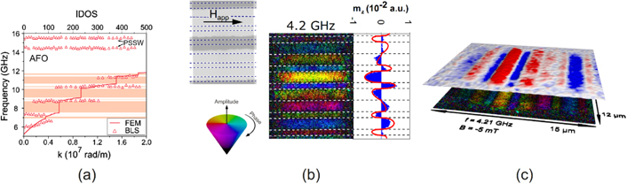
Figure 4. A magnonic quasicrystal, consisting of permalloy stripes arranged in a Fibonacci sequence. (a) Integrated density of states measured by BLS and calculated by FEM. (b) STXM measurement of the spin wave phase and amplitude at an excitation frequency of 4.2 GHz. (c) 3D rendering of a snapshot of the out of plane magnetization component mz of the STXM movie. Reproduced from [30]. CC BY 4.0.
Download figure:
Standard image High-resolution imageAt the same time as experimental techniques like BLS, MOKE microscope, scanning transmission x-ray microscopy (STXM) and electrical spectroscopy evolved and got optimized for magnonics research, analytical and computational techniques were developed to fully capture MCs. Prominently, these include plane-wave theory for two- and three-dimensional systems [33] and extensions were also found for quasiperiodic systems [30]. These proved to be especially powerful, as they allow for modeling of large systems that had been computationally prohibitive for micromagnetic simulations; while the latter focused on ultra-nanoscale systems to deepen fundamental understanding MCs with strong magnonic modulation.
However, research into MCs goes beyond being yet another wave in a periodic potential. Contemporary micro- and nanolithography allows precise spatial patterning on the length scale of wavelength, while observation techniques like BLS [31] or more recently STXM [30] allow direct imaging of the spin waves themselves (cf figure 4). Furthermore, exchange, magnetostatic, anisotropy energies are main factors shaping the dispersion relation and their tunability provide an extensive playground for new physics.
2.2. Current and future challenges
Quasiperiodicity offers new dimensionality in design of collective spin-wave excitation spectra. The discrete spectra feature self-similarity provide extended and localized states. Localized waves controlled by the magnetic field orientation were already detected. They promise for short wavelength wave excitation and broadband RF operation, yet, future studies need to demonstrate such quasiperiodic utility. Here, the influence of extended coupling of elements separated by large distances, negative group velocity, non-reciprocity, and chirality provide a test bed for new ideas, hardly accessible for other types of waves. The combination of these features with quasiperiodicity awaits discovery.
Moving toward the third dimension is a topic in many branches of solid-state physics and technology, from microelectronics, through photonics to magnonics. Thinking beyond planar magnonic structures, the third dimension can be exploited to control the in-plane propagation of spin waves, offering a robust route for designing nonreciprocal magnonic spectra with chiral properties without the need for DMI and sophisticated material growth. In MCs it can be further exploited to control in-plane coupling between the patterned elements, enhancing the group velocity and non-reciprocity; and guiding the waves in circuits for magnon spintronic applications. This bottom-up approach can be continued toward forming full magnonic 3D crystals (see section 6). New deposition approaches, like focused electron beam induced deposition and atomic layer deposition, offer fabrication of various 3D shapes in a periodic arrangement. Due to their shape anisotropy and small size, their magnetic elements are in a monodomain state and can work as discrete magnetic dipole arranged in a 3D lattice [22].
A further 3D design aspect is artificial spin ice systems with frustration at the vertexes of the elements. This is still a big challenge as even in planar artificial spin ice, the collective dynamics and guiding spin waves along controllable paths are in an infancy state of development [34, 35]. A real breakthrough is needed to provide a feasible approach for controlled coupling between spin wave dynamics of nearest, but also next- and next-next-nearest elements to achieve collective excitation in the whole array.
For the realization of sophisticated magnonic lattices with extended tunability, advances in preparation techniques are necessary to move beyond the strong modulation used in the past (see section 1). Thus, mild and gradual techniques for changing saturation magnetization, anisotropy, and damping are needed (see section 12). First steps toward this end have been undertaken in terms of doping or thermal gradients; additional promising approaches include localized strain modulation (see section 8), graded and combinatorial material deposition [36].
Furthermore, magnetic textures could be envisioned to also achieve such mild modulations. To this end, it has been shown that magnetic force microscopy tips and soft x-ray beams can be used to write arbitrary magnetization textures in specific materials [37]. This brings us to another broad area in the future of magnonics, which is the control of spin waves by magnetization textures rather than material structuring. In this case, the spin waves can follow paths designed on demand by a local change of the magnetization texture (see section 11). This is also true for periodic and other types of regular magnetization patterns, like stripe domains, and well forgotten bubble domains. The sign of possible magnonic band structure formation in stripe domain structures in multilayers with PMA has been shown.
Another approach toward reconfigurable MCs are controllable modulators. These prepatterned structures modulate the potential for magnons by a non-magnetic stimulus like a current or voltage (see section 18). First steps in this direction have been taken by utilizing superconductor hybrids and mediation by magnon–fluxon interaction [38] (see section 21). This opened up a vast field of control effects like piezoelectricity or VCMA and control mechanisms that have quasiparticle–magnon interactions for future research.
Chern numbers and Zak phase describe the topology of the crystal's bands. Whenever the sum of the Chern numbers of the bands up to the band gap edge differ from zero, the states localized at the edge of the MC are topologically protected [39]. This property, common for other types of waves, has been predicted theoretically for magnonics, but is awaiting experimental demonstrations. The wealth of magnetization textures in magnetic material makes magnonics most suitable to offer reprogrammable topological properties for guiding waves (see section 20).
Vortex and skyrmion lattices were and are, respectively, hot topics in magnetic community. Their collective excitations can be tuned and shaped in a broad range, however the transmission of spin waves through these complex textures is so far limited due to scattering and damping. This loss is a bottleneck in the study and potential applications of MCs, especially in metallic films. Just recently, the technology for patterning of insulating ferromagnetic samples has been developed offering structure sizes below 100 nm, but still low magnetization saturation limit some potential applications [39]. Traditional antiferromagnetics as well as SyAFs may offer a viable alternatives for RF applications, because they feature higher operation frequencies and CMOS compatible processing, respectively.
However, when adding gain, for instance by external microwave field, these systems can preserve parity-time (PT) symmetry, and the loss starts to play significant role. In photonics the PT-symmetry and breaking PT-symmetry opened the large area of new physics, with fascinating exceptional points were the dispersion branches start to overlap. In magnonics, this research has just started and it can be expected to become some of the leading directions in the coming years. Additionally, to patterned structures, the gain-loss will be explored in stripe domains and other regular magnetization textures. Moreover, nonlinearities and their periodicity in space and time will be exploited in the context of MCs. Recently, the existence of magnonic space time crystals has been observed [32]. In analogy to conventional MCs, it can be expected that they form a band structure in space and time, that offers additional degrees of freedom.
2.3. Concluding remarks
While ferromagnetic films with periodic corrugation for steering spin waves were introduced in the seventies of the previous century, but band properties of spin waves were investigated only from the beginning of the 21st century. This strongly contributed to the rise of magnonics as emerging field in physics and technology. The richness of ways for magnetic film modulation—including patterning, modulation with ions or light, complex magnetization textures—make wave dynamics in MCs an intriguing topic of research. Fascinating aspects like negative group velocity, anisotropic dispersion relation, chirality and nonreciprocity, topology in dynamics mixed with topologically protected static magnetization configuration, reconfigurable textures, and different types of interactions can be immersed into one magnonic system. A uniqe combination of this vast toolbox of parameters for control and direct observability of spin waves exerts a fascination on fundamental researchers and makes MCs and quasicrystals a prospective topic of research.
Acknowledgments
MK has received financial support from the National Science Center of Poland (Project Number UMO-2018/30/Q/ST3/00416). JG acknowledges financial support by the Federal Ministry of Education and Research of Germany in the framework of DynaMAX (Project Number 05K18EYA).
3. Magnonic circuits
Christoph Adelmann1, Sorin Cotofana2 and Azad Naeemi3
1Imec, Leuven, Belgium
2Delft University of Technology, The Netherlands
3Georgia Institute of Technology, United States of America
3.1. Status
In the last decade, tremendous progress has been made in the field of magnonic logic devices and gates [40]. The current status and the roadmap for devices are summarized in section 4. Various spin-wave-based logic devices have been proposed and experimentally demonstrated, e.g. interferometer-based logic gates [41] or spin-wave majority gates [42–44]. Practical applications of such logic devices and gates will however require their combination in circuits and, ultimately, in computing systems containing both logic and memory. Yet comparatively little work has been devoted to magnonic circuits and systems [22, 42, 45, 46]. Currently, no complete proposal of a realistic 'magnonic computer', including magnonic logic circuits, magnonic interconnects, and magnonic memory, exists and it is unclear if magnonics can competitively replace all aspects of state-of-the-art charge-based computing systems.
Beyond logic gates, interconnects are the key elements of any circuit. Interconnects transport signals to cascade different gates or provide clock as well as power. In today's circuits based on CMOS technology, more energy is typically dissipated in interconnects by moving data around rather than in transistors by processing information. The fraction of the power dissipated in interconnects may be even larger for spin-based logic if communication happens via spin currents, domain wall propagation, or by converting back and forth spin signals to electrical signals [47]. In magnonic circuits, it is natural to employ spin waves as information carriers. However, when compared to electromagnetic waves, spin waves are slow and lossy, and as such communication over large distances cannot be competitive with electric or optical interconnects. On the other hand, in magnonic circuits, the boundary between computation and communication may disappear. If losses can be kept under control, communication may not require extra energy cost. Unlike optical waveguides, magnonic circuits can scale to nanoscale dimensions. Currently, these considerations point toward a hybrid systems concept with local spin-wave islands embedded in a CMOS periphery (see figure 5).

Figure 5. Block diagram of a hybrid spin-wave–CMOS system including a spin wave circuit as well as a CMOS periphery to enable the usage of voltage signals for input and output. © [2014] IEEE. Reprinted, with permission, from [45].
Download figure:
Standard image High-resolution imagePrevious benchmarking of such hybrid spin-wave–CMOS systems has suggested substantial potential for power reduction with respect to CMOS [45–47] if the signal conversion between magnonic and electric domains can be sufficiently efficient. This indicates that magnonic logic circuits may find application in future ultralow power electric systems. Moreover, such hybrid systems have potential for area reduction even for relaxed lithography specifications, hence potentially reducing cost. The main drawback of magnonic circuits is that they can be expected to be considerably slower than CMOS circuits, although they may still outperform current CMOS counterparts in terms of the area-delay-power product (ADPP) [46].
Currently, no experimental proof-of-concept magnonic circuits have been realized. Missing elements are efficient transducers to convert signals at the inputs and outputs of the magnonic circuit between the spin-wave domain and the charge- or voltage-based periphery, and methods to restore signals in magnonic circuits to compensate for spin-wave amplitude variations. In these fields, substantial advances are required to realize the prospect of hybrid spin-wave–CMOS systems for microelectronic applications.
3.2. Current and future challenges
To progress from magnonic logic devices and gates to circuits, many challenges lie ahead that must still be overcome. Challenges exist in the magnonic circuits themselves, at the interface between magnonic and CMOS parts of the system, as well as in the CMOS periphery.
The design of spin wave circuits using a set of logic gates requires that the gates satisfy several criteria. The logic gates need to be cascadable, i.e. the output signal of a gate must be usable as input signal for a subsequent gate. In typical circuits, logic gates need to be connected to several subsequent gates, requiring fan-out as well as gain. The logic levels must be robust and should not degrade within the circuit, i.e. 0 and 1 logic levels should remain clearly separate. Finally, the calculation in a circuit should be unidirectional and spin-wave logic gates should not be influenced by signals propagating backwards from the output toward the input ports (input/output isolation).
Currently, concepts of spin-wave logic gates do not satisfy (clearly) all the above criteria and therefore, the realization of practical complex spin-wave circuits has remained elusive. The main challenges to realize magnonic circuits concern the propagation of spin waves as well as the cascading of logic gates. During propagation, spin waves attenuate due to magnetic damping and therefore the logic signal degrades. This limits the length of interconnects, increases power dissipation, and ultimately determines how many logic gates can be cascaded in a circuit. Ideal materials for such logic gates combine very low losses with fast spin-wave group velocity and the ability to be co-integrated with CMOS on a Si wafer. To scale the logic gates footprint, the spin waves have to propagate in nanoscale waveguides within potentially complex geometries, which may also lead to losses e.g. when spin waves propagate around bends. If several interconnect layers are required, spin-wave vias are required that transmit information between the different layers. Propagation losses can be compensated by repeater stages or amplifiers, which however increase clocking complexity and dissipate additional energy, therefore increasing the overall energy consumption of the circuit and system. No ultralow energy repeater or amplifier has been experimentally demonstrated to date.
In addition, many spin-wave-based logic gate concepts are not directly cascadable, e.g. due to the usage of hybrid charge-spin-wave signals [40, 41] or ill-defined output amplitudes for majority gates using phase encoding [40–42]. While fan-out can be achieved by suitable gate designs (see figure 6(a)) [48], spin-wave logic gates are typically passive and do not show gain. Gain can be achieved by spin-wave amplifiers or in signal repeater concepts, although at the expense of additional energy consumption. The development of a complete cascadable spin-wave circuit concept is one of the key challenges in this field.

Figure 6. (a) Fan-out enabled spin-wave majority gate with four inputs (I) and two output (O) ports. Reproduced from [48]. (b) Non-volatile clocked spin-wave interconnect using metastable nanomagnets to detect spin waves with phase sensitivity. Reproduced from [50]. CC BY 4.0.
Download figure:
Standard image High-resolution imageA second major challenge is the efficient transduction at the interface between spin-wave- and charge-based domains of the system. Conventional approaches to generate spin waves using inductive antennas are neither efficient nor scalable. Magnetoelectric transducers based on the coupling between spin waves and voltage signals using multiferroics or piezoelectric/magnetostrictive compounds have been proposed as much more efficient transducers but significant experimental progress is still needed to demonstrate both their scalability as well as their energy efficiency. Such devices are rendered even more complex due to the targeted nm scales and GHz frequencies. In addition to generation, also the detection of spin waves is still a major challenge. Spin-wave transducers typically generate weak electric signals, and require sensitive detectors, e.g. sense amplifiers, which are however power-hungry [49]. In addition, transducers need to be able to read the result of the magnonic circuit sufficiently rapidly to limit additional delays. This will also require large transducer signals compatible with CMOS circuits to improve the signal-to-noise ratio. Alternatively, spin waves can be detected by switching a metastable nanomagnet (see figure 6(b)) [50]. Simulations have indicated that this can also be sensitive to the spin-wave phase even in the presence of thermal noise. However, major breakthroughs in material growth and processing are needed before such concepts can be realized experimentally.
Finally, the design of peripheral CMOS circuits that interface efficiently with magnonic circuits is only emerging. This work will have to go hand in hand with the development of transducers and future breakthroughs will be needed to obtain an efficient environment, in which magnonic circuits can be embedded. This research topic has been less in the focus of interest than the magnonic circuits themselves; however, it will be equally critical for the realization of the vision of magnonic circuits integrated in commercial ultralow power applications.
3.3. Concluding remarks
Currently, we believe that there are three major challenges that need to be overcome before magnonic logic can be integrated alongside CMOS in practical microelectronic applications. Present concepts for magnonic logic gates need to be completed to satisfy the necessary criteria for circuit design. Energy-efficient scalable transducers need to be demonstrated to enable low-power generation and detection of spin waves in scaled waveguides. Finally, an efficient periphery needs to be developed so that the transducers and magnonic circuits can interface with the larger CMOS part of a chip. Recent benchmarking suggests that such hybrid spin-wave–CMOS circuits and systems show great promise for ultralow power applications, which is a clear motivation for research to overcome these challenges [40, 45, 46].
Acknowledgments
CA's and SC's contributions have been funded by the European Union's Horizon 2020 research and innovation program within the FET-OPEN project CHIRON under Grant Agreement No. 801055. CA acknowledges support by imec's industrial affiliate program on beyond-CMOS logic. AN's contributions have been supported by Intel Corp. under Grant Agreements SRC Intel-MSR 2011-IN-2198 and spin interconnects-2616.001.
4. Magnonic logic, memory and devices
A V Chumak1, A Khitun2, D E Nikonov3 and I A Young3
1University of Vienna, Austria
2University of California Riverside, United States of America
3Intel, United States of America
4.1. Status
The increasing challenges with further CMOS scaling down have stimulated a great deal of interest in novel logic devices and architectures. Spin-wave data processing offer one of the promising directions toward charge-less future circuitry [40]. The unique physical and technological aspects inherent to spin waves to be implemented for data processing are listed below.
4.2. Key advantages offered by spin waves for data processing
- Spin-wave bus. A spin wave is a collective oscillation of a spin system in a magnetic lattice. It is naturally confined within a magnetic media with zero likelihood to escape or to leak into non-magnetic surroundings. This feature makes it possible to build a spin-wave bus for information transfer using magnetic nano-wires similar to optical waveguides [51–53]. Moreover, since the angle of magnetization precession of a linear spin wave usually does not exceed 1 degree (as opposite to the data-storage concepts relying on the π-switch of the magnetization), a low energy is required to excite spin waves what, consequently, ensures a low energy loss during the data transport.
- Miniaturization down to atomic scale. The smallest magnonics element size is limited by the lattice constant of material and, thus, is comparable to the fundamental limitations of CMOS. Currently, the lateral sizes of the magnonics conduits made of such a complex material as YIG reached 50 nm which is around 40 lattice constants [51].
- Large coherence length and broad frequency range. Spin-waves show relatively large coherence and propagation length lpl even at room temperature (e.g., up to 1 cm in YIG of micrometre thicknesses). These properties enable the intriguing possibility of exploiting spin-wave phase in addition to amplitude for data transfer and processing for RF applications, processing of binary data, and unconventional computing. In nanostructures, the spin-wave propagation length is usually limited to tens of micrometers. Nevertheless, considering the recent progress in the miniaturization of spin-wave wavelength λ below 100 nm (see section 7 of this roadmap), lpl might constitute up to 200 μm in YIG [54]. The smallest wavelength of a spin wave is limited by the lattice constant of material and the further miniaturization enables access to the THz magnonics (see section 14). The increase in the spin-wave frequency results in the decrease of its lifetime (e.g. linearly according to the Gilbert model). However, the group velocity υgr = dω/dk of the exchange spin wave ω ∝ k2 increases linearly with the increase in k. Thus, the ratio of the spin-wave propagation length lpl to the wavelength lpl/λ, which is the most important parameter in the wave-based data processing, stays constant at a level of around three thousand for YIG [54] or one hundred for CoFeB [40].
- Manipulation, dynamic control and reconfigurability. Among others, spin-wave dispersion depends on the magnetic field, the magnetization of the material, and on the geometrical sizes of the magnetic element. This fact translates in the possibility of the static and dynamic control of spin waves (see e.g. sections 2 and 12), for the realization of non-volatile reconfigurable magnonic elements using nano-magnets (see figure 7 ), and for the realization of magnetic bit read-in and read-out [40, 50, 52].
- Energy-efficient spin-wave to voltage converters and magnetoelectric transducers. There is a robust and energy-efficient mechanism for spin-wave to voltage and vice versa conversion, using multiferroic cells [40, 50, 52] (see also sections 3, 8 and 18). This approach is of great importance for integrating spin-wave devices with conventional electronic components and for the integration of memory cells into magnonic circuits (see figure 7(c)).
- Efficient nonlinear magnon phenomena. The processing of data, in general, requires the utilization of elements with nonlinear characteristics that are, e.g., provided by a semiconductor transistor in CMOS. The pronounced benefit of spin waves for the data processing is their pronounced natural nonlinearity that allows for an all-magnon control of one magnonic unit by another to realise integrated magnonic circuits [53].

Figure 7. A two-bit magnonic holographic memory [57]. Magnonic holographic image of two cobalt magnets on ferrite waveguide. The red markers show experimentally detected inductive voltage in millivolts produced by four interfering spin waves. The cyan surface is a computer reconstructed 3D plot. (b) Schematics of the magnet configuration. The operational frequency is 3.4 GHz. All experiments are done at room temperature. © [2015] IEEE. Reprinted, with permission, from [57]. We utilize spin waves for the parallel read-out of magnetic bits. (c) Illustration of a clocked three-stage cascaded spin-wave device comprising of: a charge to spin (C–S) converter, intermediate spin-wave repeaters and spin-wave interconnects. Reproduced from [50]. CC BY 4.0. The sequential switching of the converter and the repeaters is accomplished via application of clocks 1–4 while the input data is applied in the form of current pulses using the STT clock.
Download figure:
Standard image High-resolution image4.3. Classes of magnon devices
- Spin-wave RF applications. Spin-wave frequencies cover the range from sub-GHz up to hundreds of THz. Modern state-of-the-art technology usually covers the frequency range of up to 100 GHz which is of special interest for the upcoming 5G communication systems. Different devices have been proposed, including reconfigurable filters (e.g. based on MCs discussed in section 2), delay lines, phase shifters, Y-circulators, multiplexers, wake-up receivers, signal-to-noise enhancers, and spectrum analysers [55] (see also section 9). The nano-sized spin-wave directional coupler realised recently is also a universal RF data processing unit with multiple functionalities [53].
- Interference-based Boolean logic and majority gate. Most of the developed spin-wave Boolean logic gates exploit spin-wave phase to perform operations. The Boolean data can be encoded into spin-wave amplitude, and the constructive or destructive interference allows one to obtain logic '1' (a certain amplitude) or '0' (zero amplitude). This approach has recently been used for the realization of XNOR logic gate based on a 54 nm thick YIG interferometer (see figure 8 (a)) [56]. Another way is to encode Boolean data into spin-wave phase rather than amplitude. It is especially successful for the realization of logic majority gates (see also section 3). This logic device usually features a three-input combiner with the logic information encoded in a phase of 0 or π of and the phase of the output signal represents the majority of the input phase states. Recently, a reconfigurable nanoscale inline design without the spin-wave combiner majority gate was realized at the nano-scale (see figure 8(b)) [44]. It has been shown, that the interference-based computation allows for frequency-division multiplexing as well as the computation of different logic functions in the same device.
- All-magnon circuits. The two-way conversion of magnonic signals to electric is always associated with parasitic loss and the 'all-magnon' data processing aims to process as much information purely within magnonic system as possible without its conversion to electric signals. This is the main idea behind the original work on magnon transistors. The converters in this approach are replaced by spin-wave nonlinearity and amplifiers. Recently, a nanoscale magnonic directional coupler has been realized experimentally (see figure 8(c)). This coupler was used to design and investigate numerically a first integrated magnonic circuit in a form of half-adder [53]. The half-adder consists of three magnetic nanowires and spin-wave amplifier, and replaces 12 to 20 transistors in various CMOS implementations.
- Unconventional spin-wave computing. Here we would like to report on the significant progress in spin-wave logic and memory devices prototyping since the first publication [52]. The most notable results include a two-bit magnonic holographic memory where spin waves were exploited for magnetic bit parallel-read-out (see figures 7 (a) and (b)) [57]. Multi-terminal spin-wave devices were used for special type data processing in the following studies. The feasibility of data encoding in the phase combination of input spin-waves has been demonstrated. The recognition of the input pattern is accomplished by measuring the inductive voltage produced by the interfering spin waves. The first example of reversible spin-wave logic gates was demonstrated using the unique spin-wave dispersion characteristics [58]. The utilization of phase in addition to amplitude has demonstrated great potential in application to NP-problems. For instance, prime factorization was accomplished for N = 15 using spin-wave interferometer [59]. In general, spin wave approach is promising for finding the period (∼100) of a given function. Another approach of the unconventional spin-wave data processing is Fourier magnonics described in section 9.
- Inverse-design magnonics. Many magnonic devices were demonstrated, but the development of each of them requires specialized investigations and, usually, one device design is suitable for one function only. Inspired by the recent progress in photonics, an inverse-design magnonics was proposed by two groups independently [60, 61]. In this concept, any functionality can be specified first, and a feedback-based computational algorithm is used to obtain the device design. The proof-of-concept prototype [60] is based on a rectangular ferromagnetic area which can be patterned using square shaped voids. To demonstrate the universality of inverse-design magnonics, linear, nonlinear and nonreciprocal magnonic functionalities were explored and used to realize a magnonic (de-)multiplexer, a nonlinear switch and a circulator. The prototype [61] represents a neural network, where all neuromorphic computing functions, including signal routing and nonlinear activation are performed by spin-wave propagation and interference.
- Neuromorphic magnon computing. It is expected that spin-wave circuits will manifest advantages compared to nanoelectronic devices outside of traditional Boolean computing architectures especially in neuromorphic computing [61, 62]. Spin waves possess all key ingredients: (i) a possibility to construct complex 2D and 3D networks [40, 53, 56, 57] (see also sections 3 and 6), (ii) offer a variety of nonlinear phenomena [53], and (iii) computing units can be complemented by memory cells [50]. A magnon adder, which integrates over incoming spin-wave pulses in an analog fashion, was investigated numerically [62] and represents one of the key building blocks for future magnonic neuromorphic networks. Recently, a nanoscale neural network based on the utilization of non-linear spin-wave interference was developed by means of inverse-design approach [61].
- Magnon quantum computing. One of the main advantages of magnonics is that novel efficient data processing concepts can be realized at room temperature. Nevertheless, the decrease in temperature down to <100 mK freezes out thermal magnons and allows for the data operations with single magnons. This opens an access to the entangled magnon states and to quantum computing. Currently, the field of magnon quantum physics is at the very beginning of its way (see section 19), but the group of Nakamura from the University of Tokyo has reported on the operations with single magnons in a set of recent publications. Further aspects of cryo-magnonics are overviewed in section 21.
4.4. Benchmarking of spin-wave circuits
The theoretical framework for benchmarking beyond-CMOS devices and circuits [63] included spin-wave devices. One of its conclusions applicable to spin-based devices in general is that they can be competitive with nanoelectronic devices when relying on magnetoelectric transduction (rather than spin torque or magnetic field). The transduction-based approach has advantage that it can be combined with existing CMOS circuits and does not require the development of a novel type of circuitry. One option for it is the piezoelectric-magnetostrictive transduction. The all-magnon data processing approach, was benchmarked in reference [53]. It was found that 30 nm-based magnonic circuit is comparable to 7 nm-based CMOS in terms of footprint, has 10 times smaller energy consumption, but is slower. The further magnonic circuits benchmarking is discussed in section 3 (figure 8).
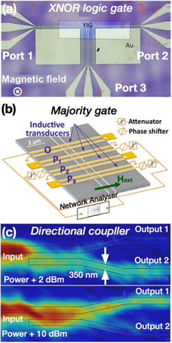
Figure 8. Micrograph of three-port logic XNOR gate using forward volume spin wave interference in a 54 nm thick YIG structure. Reproduced from [56]. CC BY 4.0. Two spin waves are injected by ports 1 and 2. The output signal is defined by the interference of these two waves and is measured at the port 3. (b) Scanning-electron micrograph of a in-line spin wave majority gate with an 850 nm-wide Co40Fe40B20 waveguide, three input antennas, and one output antenna. From [44]. Reprinted with permission from AAAS. Operation frequency is 13.9 GHz, magnetic bias field 80 mT. The input signals are injected by the antennas P1, P2 and P3. The interference of these three waves is measured at the antenna 'O'. The functionality and reconfigurability of the device are shown using all-electrical spin wave spectroscopy. (c) Nonlinear switch functionality of nano-scale directional coupler. Reprinted by permission from Springer Nature Customer Service Centre GmbH: [Springer Nature] [Nature Electronics] [53] (2020). The directional coupler is depicted with a dashed line and is based on 350 nm wide and 80 nm thick YIG waveguides. The color maps represent two-dimensional spin-wave intensity measured by BLS spectroscopy for different input powers of 2 dBm (top) and 10 dBm (bottom). The nonlinear switch of the spin wave path to output 1 or output 2 by the change in the spin wave amplitude is clearly visible. This functionality allows for the realization of complex all-magnon circuits.
Download figure:
Standard image High-resolution image4.5. Current and future challenges
Although we observe drastic progress in the evolution of the spin-wave circuitry and, in particular, its scaling down from mm to sub-100 nm sizes, many challenges still have to be addressed. Spin-wave damping remains one of the major problems for the spin-wave circuitry. Most of the above-mentioned prototypes were realized on the base of YIG material grown on GGG substrate, as the material with the smallest damping. The attempts to switch to YIG on silicon have not been successful as the damping increases significantly. The utilization of new magnetic materials, e.g. CoFeB or Heusler compounds, grown on Si attracts interest.
A cross talk between input and output ports is a big challenge for spin-wave devices using conducting contours for excitation/detection. Another reason staying behind the low efficiency of generation and detection of spin waves, is the impedance mismatch between the electromagnetic waves and spin waves related to momentum mismatch. The mismatch suggests using a periodic magnetic or piezoelectric transduction structure, or possibly acoustic-wave mediated transduction. Novel transduction geometries are required here. In this context, the demonstration of switching of non-volatile magnetic elements by spin waves as proposed e.g. in [50] is highly an important result (see figure 7(c)). Moreover, there are many approaches which allow for the unidirectional propagation of spin waves (see e.g. section 16) and can ensure input/output isolation in circuits.
The all-magnon approach does not require converters but relies on the voltage controlled magnetic anisotropy (VCMA) parametric amplifiers (see section 18) that were studied theoretically but not yet realized experimentally. Moreover, the simulated half-adder appeared to be slower compared to CMOS [53] suggesting the need in the increase of operating spin-wave frequencies up to the sub-THz or THz ranges.
4.6. Concluding remarks
It was shown numerically that ME-cell based spin-wave logic circuits can overcome a 10 nm CMOS implementation by up to 100 times in terms of the ADPP (see section 3). This is the reason why the main attention of the magnonics research community is focused nowadays on the realization of high-efficiency magnon-to-current converters. The all-magnon circuits approach also has shown that can be competitive to CMOS in terms of footprint and energy consumptions. These achievements are very encouraging and suggest the utilization of the developed concepts and approaches for their further utilization in much more powerful unconventional, neuromorphic and quantum computing concepts instead of Boolean ones. As was shown, unconventional spin-wave logic circuits promise an intriguing possibility of constructing multi-functional logic architectures with built-in memory, pattern recognition, prime factorization and others. Particularly these unconventional computing concepts at the nano-scale utilizing the powerful nonlinear spin-wave physics have a large potential to compete with CMOS and to occupy its niche in specialized types of computing applications.
Acknowledgments
AVC acknowledges financial support by the European Research Council Starting Grant 678309 MagnonCircuits.
5. Magnon Bose–Einstein condensation and supercurrent transport
Vitaliy I Vasyuchka and Burkard Hillebrands
Department of Physics and State Research Center OPTIMAS, Technische Universität Kaiserslautern (TUK), Kaiserslautern, Germany
5.1. Status
Novel physical phenomena constitute a driving force for the successful development of the fascinating and dynamic field of magnonics. One very promising direction is the investigation and utilization of magnon macroscopic quantum states. Magnons are bosons, and thus they are able to spontaneously form a spatially extended, coherent macroscopic quantum state—magnon Bose–Einstein condensate (BEC) [64]. The magnon BEC in a magnetic medium is established as one single quantum state with the lowest energy as a result of the thermalization process in an overpopulated magnon system. The condensation of magnons can occur even at room temperature due to specific properties of magnons as such as the small effective mass, nonlinearity, a large number of thermal excitations at non-zero temperatures, the simplicity of the magnon injection into a magnetic system and control of their population.
During the last decades, many efforts have been made to observe the magnon condensation in solids. One of the best examples of a magnetic medium, where the magnon BEC was achieved, is the insulating ferrimagnet YIG possessing an extremely low magnetic damping. The main approach to reach the magnon BEC in YIG was based on the increase of the magnon density above the thermal equilibrium level. Just a few percent excess of magnons over their thermal level is sufficient to achieve the condensation in YIG. For this, various methods of magnon injection into YIG have been employed (see figure 9). Here, the most interesting studies related to magnon BEC formation are listed.

Figure 9. Schematic illustration of different mechanisms leading to the formation of magnon Bose–Einstein condensates in magnetic solids.
Download figure:
Standard image High-resolution image5.1.1. Microwave parametric pumping
The most effective and popular way to increase the density of magnons to reach the magnon BEC is parametric pumping. When the applied strong microwave electromagnetic field exceeds a threshold value, the conversion of microwave pumping photons into magnons at half of the pumping frequency occurs. The majority of the magnon BEC experimental investigations were conducted using the parametric pumping technique (see e.g. [64–66]). It is important to note that the magnon condensation in an overpopulated magnon gas is also a threshold process. Typically, it happens in YIG films, when the applied pumping power exceeds the threshold of parametric pumping by two or three orders of magnitude.
5.1.2. Kinetic instability regime
Usually, the formation of the magnon condensate is accompanied by multistep cascade processes of magnon–magnon scattering events, which transfer parametrically pumped magnons down to the bottom of a magnon spectrum. Recently, it was demonstrated that the kinetic instability process provides favourable conditions for a more efficient magnon condensation process compared to the cascade-only scenario [67]. In this regime, the direct one-step transfer of the parametrically injected magnons to the lowest energy states surpasses the multistep scattering process and is followed by a thermalization of low-energy magnons into the BEC state.
5.1.3. Spin pumping via spin-Seebeck effect
A novel method of magnon injection, based on the process of spin pumping, when a spin angular momentum is transferred over the interface between a nonmagnetic metal and a magnetic material, is very promising for the formation of magnon BEC [68]. The case of the spin Seebeck effect is especially interesting [69], when a magnon flow is generated by a temperature gradient across the interface between a nonmagnetic metallic layer and a magnetic insulator. It has been demonstrated for the case of YIG/Pt nanowires, cooled to cryogenic temperatures, that the magnon current induced by the spin Seebeck effect leads to excitation of YIG magnetisation auto-oscillations and generation of coherent microwave radiation [69]. This achievement paves the way for the spin-caloritronic-based magnon BEC.
5.1.4. Rapid cooling mechanism
Very recently, a new and universal approach to enable BEC of magnons by rapid cooling has been demonstrated [70]. For this, a disequilibrium of magnons with the phonon bath is introduced via heating of a magnetic sample to an elevated temperature with a following rapid decrease in the phonon temperature. This decrease is very fast compared to the relaxation time of the magnon system. It results in a large excess of incoherent magnons in the system and in subsequent Bose–Einstein magnon condensation.
5.2. Current and future challenges
An extraordinary potential for the field of magnonics is the use of macroscopic quantum phenomena such as the magnon BEC for information transfer and processing. The following non-comprehensive list of items highlights the most promising directions dealing with the current challenges and simultaneously defining new problems for the future:
- (a)Magnon supercurrents: due to its zero group velocity, the magnon BEC cannot be directly utilized for the transport of a spin information in space. However, the information transfer can be realised by means of magnon supercurrents, which constitute the transport of angular momentum, driven by a phase gradient in the magnon-condensate wave function. The creation of such a supercurrent was experimentally successful by introducing a time-dependent spatial phase gradient into the wave function of the magnon BEC [66]. The temporal evolution of the BEC formed in a parametrically populated magnon gas was studied via BLS spectroscopy in room-temperature YIG films. It has been found that local heating in the focal point of a probing laser beam leads to the excessive decay of the freely evolving BEC, which is a fingerprint of the supercurrent efflux of condensed magnons. An additional indirect confirmation of the existence of magnon supercurrents was obtained through BLS observations of quantized vortices in a two-component Bose–Einstein condensate [65].
- (b)Excitations in magnon condensate and second sound: investigations of wave-like excitations that propagate in condensed and in normal phases of a magnon gas pose another intriguing challenge. They may pave the way to a complementary approach for spin information transfer. Recently, it was demonstrated that the condensed magnons being pushed out of the locally heated area form compact density humps, which propagate over long distances through a thermally homogeneous magnetic medium [71]. They were understood as a superposition of Bogoliubov waves with oscillations of both the amplitude and the phase of the magnon BEC's wave function. These waves are described by a linear dispersion law in the long-wavelength limit and can be considered as a magnon second sound of the condensed magnon phase.
- (c)Magnonic Josephson effects: by analogy to the Josephson effects in superconductors, both the alternating current (ac) and the direct current (dc) magnonic Josephson effects were proposed and studied theoretically [72]. A junction connecting two weakly coupled quasi-equilibrium magnon BECs is an essential component for the observation of these fascinating phenomena. The first step in the experimental realisation of the ac magnonic Josephson effect was recently reported in the system of two room-temperature magnon condensates separated by a magnetic trench [73]. Josephson oscillations of the magnon BEC density in the trench were observed, which are induced by the coherent phase shift between the two magnon condensates from the left and right zones of this magnetic inhomogeneity. Further developments within this challenge would facilitate the broad application of magnonic Josephson effects for data processing in magnonic devices.
- (d)Electric control of magnon supercurrents: the possibility of electric control of magnon supercurrents using the magnonic Aharonov–Casher effect, which has so far been analyzed only theoretically [72], is extremely appealing. It is predicted that this effect will lead to the generation of a persistent magnon supercurrent in a magnetic ring subjected to an electric field with the radial symmetry due to the accumulation of an induced Aharonov–Casher phase in the magnon condensate. The long-distance coherency of the magnon condensate is of paramount importance to the observation of the magnonic Aharonov–Casher effect.
- (e)Computing with magnonic macroscopic quantum states: nowadays, an exceptional and promising challenge is the utilization of magnonic macroscopic quantum states for information processing and computing. Activities in this direction, in particular those related to experimental implementation, are in their initial stages and research in this area is in great demand. The question of quantum computing with magnon condensates remains especially interesting.
The following scientific and technological advances can help to overcome many of the specified challenges: magnetic materials with exceptionally low damping, involvement of the interface effects particularly for the nanometer-thick magnetic films, better understanding of the quantum nature of magnon BEC, and the realisation of the magnon-condensate-based qubit.
5.3. Concluding remarks
Although investigations of the magnon macroscopic quantum states are in their initial stages, this exciting research field demonstrates a continuing progress in the formation, control and usage of magnon Bose–Einstein condensates and supercurrents. Among the latter achievements, we can recognise the different ways of magnon BEC formation, spin information transfer using magnon supercurrents and second sound, novel magnonic effects, etc. Considering the richness of magnon phenomena, the wealth of nonlinear effects, the scalability and reconfigurability of magnon systems, further fruitful developments in this new branch of magnonics are expected.
Acknowledgments
Financial support of the European Research Council within the Advanced Grant 694709 SuperMagnonics 'Supercurrents of Magnon Condensates for Advanced Magnonics' is gratefully acknowledged.
6. Three-Dimensional Magnonics
Gianluca Gubbiotti1 and Sergej A Nikitov2
1Istituto Officina dei Materiali del CNR (CNR-IOM), Perugia, Italy
2Kotelnikov Institute of Radioengineering and Electronics, Russia
6.1. Status
Magnonics refers to the research field that uses spin waves, the collective excitations of ordered magnetic materials, or their quanta (magnons) as a tool for signal processing, communication and computation [74]. This field has been rapidly growing during the last decade, with magnonic systems investigated up to now mainly represented by periodic one- and two-dimensional planar systems in the form of arrays of nanowires, dots, antidots and width modulated waveguides based on insulating YIG (Y3Fe5O12), metallic permalloy (Py), CoFeB, as well as coupled structures containing also pure Ni, Co, Fe and Heusler alloys.
Very recently, due to developments in instrumentation, nanofabrication and modeling tools, researchers have devoted their attention to the fabrication 3D magnetic systems where novel physical effects comprising geometry, topology, chirality, frustration and unconventional spin textures emerge [75]. Examples of three-dimensional (3D) magnonic nanostructurescan also be found in sections 1, 11 and 12. The advantage of magnonic systems magnetic materials include the possibility to overcome the fundamental physical limit in heat generation associated with electrical current in silicon-based technology, potentially small magnon wavelengths in the range of tens of nanometers, and high-frequency operation in the terahertz regime. In addition, the interest in 3D and vertically coupled magnonic structures is based on a similar trend in CMOS electronics, as it enables a transition from two-dimensional to three-dimensional functional design for integrated structures [12].
Following this trend, researchers are proposing different strategies to build the next generation of 3D magnonic systems. The first of them is an extension of planar patterned nanostructures, where arrays of patterned magnetic dots or antidots have a layered structure. In this case, the vertical stacking of ferromagnetic materials, placed in direct contact or separated by a non-magnetic spacer, adds new functionality and an additional degree of freedom to control the spin-wave band structure based on the interplay between exchange [76] and dipolar interactions [77] as well as on the phase relation (in-phase or out-of-phase) between the dynamic magnetizations in the different layers. These also offer a valuable tool for tuning the static magnetization configuration (parallel and anti-parallel) in a reconfigurable manner and therefore reprogram the magnonic band structure on demand, as shown in figure 10 for a dense array of Py (30 nm)/Cu (10 nm)/Py (30 nm) nanowire array.
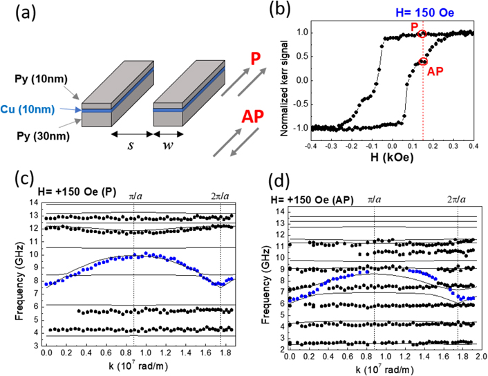
Figure 10. (a) Schematic drawing of the permalloy (10 nm)/Cu (10 nm)/permalloy (30 nm) trilayer nanowire array with width of w = 280 nm and edge-to-edge spacing of s = 80 nm. (b) Measured longitudinal hysteresis loop for the nanowire array. The vertical red dashed line indicates the field value of +150 Oe, which following either the descending or the ascending branch of the hysteresis loop, corresponds to a parallel (P) or antiparallel (AP) alignment between the magnetization in the two permalloy layers. Comparison between the measured BLS (points) and calculated (lines) magnonic band structure for the nanowire array in the P and AP states (H = +150 Oe). Reprinted (figure) with permission from [77], Copyright (2018) by the American Physical Society. The external magnetic field is applied along the nanowire length both in the MOKE and in the BLS measurements.
Download figure:
Standard image High-resolution imageOn the other hand, 3D meander-like single- and multilayer films (see figure 11(a)) grown at the top of the initially structured substrate and magnetized along the thickness steps have been proposed as a candidate for such 3D magnonics crystals for vertical steering of spin-wave beams thus allowing to overcome the difficulties of bending spin-wave beams for in-plane magnetized systems due to the anisotropic dispersion of dipolar spin waves [78]. Spin waves propagate in film's segments located at right angles with respect to each other thus making possible the wave propagation in three dimensions without significant losses in the junction region [79].

Figure 11. 3D vertical magnonic structures: (a) meander-shaped ferromagnetic film. Reprinted from [78], Copyright (2019), with permission from Elsevier, (b) YIG film grown on GaAs substrate. Reprinted (figure) with permission from [83] Copyright (2019) by the American Physical Society, (c) YIG–metal–semiconductor nonlinear shifter. Reproduced from [84]. © IOP Publishing Ltd. All rights reserved, and (d) MC sandwiched between two ferroelectric layers.
Download figure:
Standard image High-resolution imageMoreover, domain walls together with DMI can be considered as elements of 3D magnonics for propagation of spin waves in curved geometries and in close proximity to other channels [80]. Because the spin structure of domain walls is primarily governed by intrinsic magnetic properties, they are less sensitive to issues related to lithography or nanofabrication such as edge roughness or sample-to-sample reproducibility.
A very promising and alternative method to physical patterning is based on the use of hybrid heterostructures in the form of bilayer systems in which the non-magnetic component induces periodic modulation of either the static or the dynamic internal magnetic field of the magnetic film itself [12]. These include ferromagnetic (FM) metal–insulator, FM metal–heavy metal (HM), FM metal–antiferromagnet, FM metal–ferroelectric and FM metal–superconductor bilayers (section 21), for which new properties of spin waves such as confining and filtering, guiding and steering, non-reciprocity and reconfigurability, a direct and an indirect gap in the magnonic band structure, have been proved (section 16).
Finally, curved surfaces and 3D micro and nano-objects exhibit peculiar and unexpected spin textures which are normally not observed in planar nanostructures and allows for the exploitation of magnons chirality and the resulting non-reciprocity of the magnon dispersion. 3D nano-objects with micrometer size can be fabricated to study their dynamics and to couple with macroscopic microwave field. The curvature induced spin-wave non-reciprocity offers several advantages over the iDMI since it is not limited to ultrathin ferromagnetic layers and does not increase the spin-wave damping. Moreover, freestanding 3D magnonic structures are obtained by using a complex lithography process including room-temperature deposition and lift-off of amorphous YIG as well as subsequent crystallization by annealing [81].
6.2. Current and future challenges
In terms of potential applications, 3D magnonic structures might be exploited to realize complex vertical interconnection elements for efficient spin-wave transport between multiple layers inside magnonic networks. This could lead to the new development of 3D magnonics circuits mainly used for the multiple-layer architecture of signal processing devices comprising the neuromorphic principles of data processing [82]. In 3D circuits, shorter interconnects reduce the average wire length whereas the vertical dimension adds a higher order of connectivity and offers new design possibilities. Increasing the density of elements will be a crucial aspect for the realization of scalable and configurable magnonic networks and will lead to a decrease in spin-wave propagation and energy losses.
The perspectives of the practical use of 3D magnonic structures can also be based on a combination of electronics components using both semiconductor and magnonic technologies. Thus, the opportunity appears to integrate magnonic structures with spin transfer and semiconductor structures with electric charge transfer. The main problem here is to superpose at high technical level material parameters (e.g., YIG) and semiconductors (e.g. Si, GaAs,GaN, etc). Recent experiments have shown that YIG film grown onto GaAS substrates can be a good candidate for the integration of magnonics and semiconductor electronics (figure 11(b)). GaAs has a large band gap in 1.4 eV and high mobility of electrons and holes up to 8600 cm2 V−1 s−1 and 400 cm2 V−1 s−1, respectively. Making 3D structures with these materials and superimposing light from the laser one can govern the properties of spin waves and information processing [83].
Nonlinear processes originating during spin-wave propagation in ferromagnetic materials are of particular interest, since they occur at sufficiently low power levels and new types of spin-wave excitations can be implemented. The main nonlinear effect in a MC is the nonlinear frequency shift (and, respective shift of the band structure) with increasing input signal power. In 3D magnonic structures, the particular effect of 'nonlinear switching of the MC' is possible, in which periodic structure allows to pass the signal of high power at frequencies within the bandgap (figure 11(c)). This feature allows considering such 3D based on MCs as a nonlinear phase shift modulus and the noise limiters [84].
Another important aspect for 3D magnonics is the integration with piezoelectrical materials where propagating SAWs and electromagnetic waves can both interact with spin waves (figure 11(d)). Such voltage-controlled anisotropy and current-induced magnetization dynamics in magnonic/piezoelectric (and/or ferroelectric) heterostructures can be a subject for future 3D magnonics applications [85].
In the case of FM–HM multilayers, it is possible to take advantage of the unidirectional coupling induced by iDMI to transfer the information carried by the spin waves between thin ferromagnetic layers in only one direction of propagation. In this particular system, the functionality of spin-wave diode and circulator to steer and manipulate spin waves over a wide range of frequency has been demonstrated [86].
6.3. Concluding remarks
Here we have reviewed the most recent advances in 3D and vertical stacked magnonic structures and discussed some of the most interesting perspectives. We highlighted several open questions that still need addressing, such as smart methods for excitation, amplification and detection of spin waves and efficient interconnections between magnonic and electric circuits. Being aware of the difficulties and challenges related to the fabrication of 3D magnonic structure, we believe that the exploitation of the third dimension will bring to additional and specific features (e.g. vertical magnon transport, nonreciprocal coupling) while in CMOS technology the vertical stacking only gives higher storage density with the disadvantage of the standard CMOS heat problem.
Acknowledgments
The research of SAN was supported by the Government of the Russian Federation (Agreement 074-02-2018-286) within the laboratory 'Terahertz spintronics' of the Moscow Institute of Physics and Technology (National University) and by the State task 0030-2019-0013.
7. Short wavelength magnonics
Haiming Yu1 and Dirk Grundler2
1Beihang University, People's Republic of China
2École Polytechnique Fédérale de Lausanne (EPFL), Switzerland
Spin waves are considered to be promising as information carriers in low-power-consuming computing and logics with advantages such as absence of Joule heating, clock frequencies up to the THz frequency regime (see section 14: 'THZ magnonics') and coherent processing of data across several unit cells (see section 4: 'magnonic logic, memory and devices'). Spin waves with wavelengths λ at the nanoscale (figure 12) reside in the exchange-dominated regime of the spin-wave dispersion relation  in a ferromagnetic thin film. They exhibit group velocities vg = 2π df/dk which increase with decreasing λ, i.e., increasing wave vector k = 2π/λ. Such spin waves (magnons) are particularly attractive for high-speed magnonic devices and data processing. However, excitation and detection of short-wavelength magnons are non-trivial and represent a major challenge. Conventional methods based on microwave antennas such as metallic CPWs are inefficient. This is due to impedance mismatching and ohmic losses when the lateral size of the antennas shrinks down the nanoscale [87]. Several promising methods have been proposed to overcome these challenges e.g. by using resonant and non-resonant magnonic nanogratings [88], ferromagnetic coplanar waveguides (mCPW) [89], parametric pumping [90], spin-transfer torque [91] and spin textures [92].
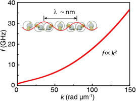
Figure 12. Dispersion for short-wavelength spin waves in YIG (20 nm thickness, saturation magnetization 140 kA m−1, exchange constant 3 × 10⁻¹⁶ m2) where the propagation direction is perpendicular to the magnetization. At large k (small wavelength λ) the dispersion relation follows a f ∝ k2 behavior dominated by the exchange interaction.
Download figure:
Standard image High-resolution imageGrating couplers with multidirectional emission and detection of short-wavelength magnons were proposed and experimentally demonstrated based on both one- and two-dimensional periodically modulated ferromagnets integrated to conventional CPWs. Individual ferromagnetic layers with etched nanotroughs (similar to antidot lattices) as well as bicomponent ferromagnetic systems consisting of arrays of overgrown nanostripes or embedded nanodisks were used to evidence the grating coupler effect on a broad spectrum of metallic ferromagnetic thin films. This versatile approach was used to excite and detect ultrashort magnons with λ = 68 nm in ferrimagnetic YIG using 2D ferromagnetic nanodisk arrays [88] and λ = 50 nm using 1D ferromagnetic stripe arrays [93] (figure 13(a)). In case of large magnon velocities thin insulating YIG offers unprecedentedly long decay lengths compared to the metallic ferromagnets [94]. In these periodic lattice-based microwave-to-magnon transducers, the Bloch theorem was exploited and the wave vectors of magnons were defined by reciprocal lattice vectors up to high orders (figure 13(a)). Their amplitudes were on the same order as the ones of long-wavelength spin waves excited directly by the conventional CPWs. The amplitudes were particularly large in case of gratings operated at their own resonance frequencies (resonant grating coupler effect) [88].
Figure 13. (a) Dispersion of short-wavelength spin waves propagating in a 20 nm-thick YIG film. The frequencies and wave vectors of the data points are extracted from the experiments on three different samples with different spin-wave modes. The red curve is the calculated dispersion f(k) with an applied in-plane field of 1000 Oe. The inset shows the transmission spectra of short-wavelength spin waves with λ ≈ 50 nm. Figure dispersion relations for propagating short-wavelength spin waves. Reproduced from [93]. CC BY 4.0. (b) (Left) sketch of micrometer-wide mCPWs consisting of Fe (brown) underneath Au (bright) on YIG. Local detection of magnons was performed through the GGG substrate using BLS. (Right) dispersion relations of magnons are shown for bare YIG (magenta) and close to the mCPW (green). The arrow illustrates the wavelength conversion. Figures schematic diagram and high-frequency modes emitted by mCPWs and wavelength conversion and magnon signal strengths. Reproduced from [89]. CC BY 4.0. (c) Dispersion of spin waves propagating in CoFeB/Ru/NiFe trilayer system, where the ferromagnetic layers are antiferromagnetically coupled through a non-magnetic spacer. Full green diamonds: experimental data obtained for spin waves propagating in the domains. Red dots: experimental data obtained for spin waves confined in the domain wall (red dots). The inset shows an STXM image taken for the data point at 0.52 GHz. The calculated dispersion (blue continuous line) and the results of micromagnetic simulations (gray dots) show good agreement [92].
Download figure:
Standard image High-resolution imageVery recently, Che et al [89] reported on magnetic CPWs (mCPWs) to efficiently excite and detect short-wavelength magnons over a broad frequency band (figure 13(b)). Here the localized stray field of an integrated ferromagnetic layer caused an inhomogeneous effective field (see also section 12: 'graded index magnonics') and induced a wavelength conversion process in YIG. The authors demonstrated continuous tuning of λ, supporting multifrequency operation of magnonic circuits. For optimized mCPWs wavelengths below 40 nm are feasible without involving nanofabrication.
Parametric pumping provides a method for spin-wave excitation where wave vectors are without an upper limitation. The wavelengths can be tuned by a magnetic field down to the sub-100 nm scale in that spin waves are excited at half of the frequency of the microwave magnetic field by a non-linear process [90]. Additionally, spin torque nano-oscillators (STNO) enable the generation of exchange-dominated magnons by spin-polarized currents overcoming the intrinsic damping. High current densities are needed and achieved by spatial constrictions. STNOs represented effective spin wave injectors for the top layer of a trilayer stack [such as a magnetic tunnel junction (MTJ)]. The wavelength of spin waves is proportional to the radius of the nanocontact [91]. The high-order modes of propagating spin waves exhibited a wavelength down to about 70 nm, which could be further decreased by a smaller radius of the nanocontacts.
Spin textures, such as domain walls and vortex cores, have also been utilized to generate short-wavelength spin waves [92] (figure 13(c)). Spin waves propagating inside spin textures and nano-sized domain walls have attracted increasing attention (see section 11: 'interaction of magnons with spin textures') and promise reconfigurable magnonic devices. For example, short-wavelength spin waves can be generated by applying an alternating magnetic field in domain walls of interlayer exchange-coupled ferromagnetic bilayers. Changing the excitation frequency, the wavelength of spin waves was tuned from 1 μm down to 150 nm in magnon conduits provided by domain walls [92]. In addition, magnetic vortex cores in an antiferromagnetically coupled magnetic heterostructure served as tuneable spin wave emitters driven by an oscillating magnetic field (figure 13(c)) [92]. In a single ferromagnetic layer, high-amplitude dipole-exchange spin waves with λ down to 80 nm have been imaged around a vortex core.
Current and future challenges for nanomagnonics.
- (a)Magnon excitation: current techniques enable the excitation of magnons in the few 10 GHz frequency regime with wavelengths of a few 10 nm, i.e., about two orders of magnitude larger than the crystal lattice constant. Future transducers should address magnons with λ below 10 nm in ferro-, ferri- and antiferromagnetic thin films. Such magnons possess high group velocities which are key to the realization of the high-speed magnonic circuits. Their properties are isotropic, thereby allowing for 3D magnonic circuits. For wave-based logic in particular coherent and phase-controlled magnons are required. A major challenge for low-power consumption lies in thin-film materials supporting the isotropic short-wave magnons in zero external field. The detection of magnons seems less challenging via e.g. spin pumping, spin-Seebeck, inverse spin Hall, or thermoelectric effects.
- (b)Direct imaging: near-field BLS already provided a lateral spatial resolution of better than 55 nm [95] and thereby detected standing spin waves beyond the diffraction of light. Recently, synchrotron-based STXM was exploited to image propagating spin waves with high spatial resolution. Laboratory-based techniques offering ultra-high spatial resolution are needed to thoroughly investigate the properties of magnons with λ below 10 nm, e.g., the scattering at structural defects and lattice vibrations. Here, magnetometry utilizing nitrogen-vacancy (NV) centers might be particularly powerful.
- (c)Antiferromagnetic spin waves: antiferromagnets are immune to external field perturbations. Their spin processional motion is not only right-circularly polarized like in ferromagnets but possesses dual polarizations due to the two-opposite magnetic sublattices. The exchange energy in the antiferromagnetic systems increases the spin wave frequencies. It is still challenging to achieve the efficient excitation and detection of coherent antiferromagnetic spin waves. Recently demonstrated spin-current generation via antiferromagnetic spin waves maycontribute for the potential applications in ultrafast magnonic devices [96].
- (d)Manipulation and control: an external magnetic field, charge currents or electrical voltages have already been used to modify or guide spin waves. All-magnon-controlled modifications open a novel route for reconfigurable magnonics [97].
- (e)Nonreciprocal transport: for the steering of signal flow nonreciprocal propagation characteristics are of great interest. A magnetic nanograting induced already unidirectional flow of magnons with λ down to 60 nm. Other experimental techniques are required to precisely control the magnon flow at small λ e.g. for diodes.
- (f)Magnon logic computing: so far, magnonic logic gates have been demonstrated mostly with long-wavelength dipolar spin waves. Major challenges exist in the transition from the single logic gate to cascaded architectures giving rise to integrated magnonic circuits. Interferometers form a key component but have not yet been realized based on phase-controlled ultrashort magnons.
- (g)Nanochannels of low damping: magnon transport in sub-100 nm wide YIG conduits has been reported only very recently [51]. Decay lengths were reduced by roughly two orders of magnitude compared to thin films [94] but magnons were excited by conventional CPWs and exhibited small group velocities. If combined with e.g. tailored grating couplers the YIG nanoconduits might support large decay lengths needed for cascaded logic gates. Non-collinear spin structures promising reduced scattering at edges and topologically protected magnon states might give rise to further nanochannels of low damping.
- (h)Quantum effects: magnons are bosons and room-temperature BEC was realized via magnons (see section 5: 'magnon-BEC and supercurrent transport'). The coherent coupling between a single magnon in a macroscopic YIG sphere and superconducting qubit in a microwave cavity was already demonstrated and opens the route for investigations on magnonics at the single-quantum level. A magnon–qubit coupling scheme involving a short-wavelength magnon is needed for integrated hybrid quantum systems.
Magnonics is rapidly evolving field and we expect more advanced methods to be proposed and tools to be developed for the coherent excitation and detection of magnons on the nanoscale. These methods are a prerequisite to gain a deep understanding of both the properties and functionalities of exchange-dominated spin waves. The tools will push the frontiers of magnonics and fuel technological prospects.
Acknowledgments
DG thanks SNSF for financial support via Grants 163016, 177550 and sinergia project 171003 Nanoskyrmionics. HY thanks the financial support from NSF China under Grants No. 11674020 and No. U1801661, and the National Key Research and Development Program of China (254).
8. Toward energy efficient magnonics: static and dynamic strain for reconfigurable spin-wave transport
A V Sadovnikov1,2, A A Grachev1, S E Sheshukova1, S A Nikitov1,2, J-Y Duquesne3 and M Marangolo3
1Saratov State University, Russia
2Kotelnikov Institute of Radioengineering and Electronics, Russia
3Sorbonne University, France
8.1. Status
The electric field controlled transfer of the magnetic moment or spin of an electron instead of charge transport opens up new possibilities to build the element base of devices for encoding and storage of information using the collective precessional motion of ordered magnetic spins–spin waves (SW) with wavelengths ranging from micrometer down to tens of nanometer with the frequencies from gigahertz to terahertz. Emerging field of magnon straintronics [98, 99] opens a promising alternative in beyond-CMOS computing technology with low-level energy consumption and minimization of Joule heating for development of next-generation devices for sensor applications and energy-saving data processing technologies focused on the generation, propagation, manipulation, channeling and commutation of information carriers.
When strain is applied statically or dynamically to a magnonic device it's possible to generate SW by acoustic waves [100], nonreciprocal propagation of SWs [101], the control of spin-wave generation and routing in lateral array of magnonic stripes and crystals [102]. These phenomena offer new way to envisage spin-wave demultiplexers and can be used simultaneously as an interconnection unit in reconfigurable magnonic networks.
The strain in the magnetic media can be produced locally by static mechanical deformations, local heating or with electric field acting on the one of the phase of the composite magnonic heterostructure which comprises magnetic and piezoelectric phase. The strain-induced physical effects in magnetic structures can be used to engineer energy-efficient complicated 2D and 3D topology of magnonic devices and heterostructures based on multiferroic materials, which exhibit electric field tunability of simultaneous ferroelectric, anti-ferromagnetic (AFM), and ferroelastic properties.
The effect of the electric field on the magnetic configuration results from the modification of the effective internal magnetic field. The latter is changed due to inverse magnetostriction (Villari effect) as a result of the local deformation of the magnetic film. This can induce a FMR frequency shift in YIG/lead zirconate titanate [Pb[Zrx Ti1−x ]O3 (0 ⩽ x ⩽ 1) (PZT)] bilayer [103]. The control of the spin-wave transport can be performed via local elastic strains by the fabrication of the system of the electrodes at the YIG/PZT interface.
The magnon straintronic approach can be used to design the magnonic logic devices with voltage control of the spin-wave amplitude and phase. From design point of view this is multistage 3D self-consistent problem. At the first stage, the finite-element calculation of elastic deformations caused by an external electric field in the piezoelectric layer is performed. Next, the obtained profiles of the internal magnetic field in the confined magnonic element are used in the micromagnetic simulation and the eigenmode spin-wave spectra calculation in the magnonic device.
In particular, strain-induced spin-wave routing was demonstrated across three adjacent magnonic stripes, which are strain coupled to a piezoelectric layer (see figure 14(a)). The strain may effectively induce voltage-controlled dipolar spin-wave interactions and results in the electric field induced spin-wave switching in the lateral array of magnonic stripes, which can be probed by means of BLS (figure 15) and microwave spectroscopy.
Figure 14. The demonstration of magnon straintronics concept: the bilateral YIG stripes (S1, S2, S3) with strain coupled PZT layer (a). The electric voltage is applied between two electrodes (VC1 and VC3) at the YIG/PZT interface and GND electrode. The distribution of stress tensor component showing a local deformation of the PZT layer and induced stress on the YIG/PZT interface (b). The voltage-induced transformation of the internal magnetic field profile (Hint(x)) (c). Left panels of (d) show the BLS spin-wave intensity at the frequency of 4.925 GHz at the different values of the applied voltages (denoted in the figure). Right panels of (d) show snapshots of the dynamic out-of-plane component of dynamic magnetization calculated by means of micromagnetic simulations. Edges of stripes are guided with dotted lines. Reprinted (figure) with permission from [99], Copyright (2018) by the American Physical Society.
Download figure:
Standard image High-resolution image
Figure 15. Left panel: SAW driven FMR in magnetostrictive element placed between two interdigital transducers (IDTs) on a single crystal piezoelectric substrate lithium niobate (LiNbO3). Li et al show in reference [100] that the resonant coupling induces SW generation and spin pumping (JS in the figure is the spin current induced by magnetization precession). Reprinted from [100], with the permission of AIP Publishing. Right panel: dispersion relation of the NiFe/Co magnonic phononic crystal calculated by Graczyk et al in reference [109]. In the color scale, blue and red correspond to acoustic and spin waves, respectively. Green indicates coupled magnetoelastic waves. Reprinted (figure) with permission from [109], Copyright (2017) by the American Physical Society.
Download figure:
Standard image High-resolution imageStrain gives us also a great opportunity to influence dynamically SW transport and even to generate SWs. As anticipated by theoretical research in late 50s the resonant coupling between phonons and magnons in heterostructures composed of piezoelectric and magnetostrictive materials lead to FMR and SW-generation. Indeed, phonons and magnons branches can cross in the (k, ω)-space either at magnetic remanence or when a moderate magnetic field is applied to a ferromagnetic material (FM), leading to modes hybridization engendered by magneto-elastic coupling (MEC) (an example is given in figure 15). The strain control can be implemented locally or globally in a continuous-wave or pulsed configuration. This interaction may lead to gap opening, frequencies shifts and tunable MC, where periodic modulation of the magnetic properties occurs at a timescale shorter than the characteristic time of SWs propagation through the crystal.
Recently, it has been shown that an efficient mean to obtain resonant MEC is by SAWs, a mature technology that has proven to tickle magnetization in thin films. By the help of interdigitated transducers (IDT) exciting SAW in the GHz and sub-GHz regime in a piezoelectric media (see IDT in figure 15), Weiler et al [104] and Thevenard et al [105] observed SAW-FMR in Ni and GaMnAs thin films, respectively. These experiments pave the way to the integration of SAW-FMR mechanism in spintronic and magnonic devices where SWs, generated by antennas or by dynamic strain could be locally handled, triggered, scattered or even suppressed by SAWs excited, in turn, by remote voltage-driven IDTs.
These SAW-FMR devices are claimed to operate with very low power, very high tunability and can benefit of the high directionality of the SW–SAW interaction [106]. Moreover, since SAWs are widely used in today's sensors, filters and microwave circuitry, the possibility to implement magnetization dynamics in this mature technology would be a worthwhile asset. An alternative way to excite acoustically SW by strain has been indicated by Cherepov et al [107]. Here, an alternating voltage excites strain waves in an multiferroic magnetoelectric (ME) cell transducers, constituted of a magnetostrictive Ni film and a piezoelectric substrate, generating spin waves.
8.2. Current and future challenges
8.2.1. Static strain for magnon straintronics
The electric-field-induced dipolar coupling between magnetic stripes leads to the formation of symmetric and antisymmetric collective modes in the spectra of propagating spin waves in lateral array of MCs, where local strain can tune the frequency of magnonic band gap and control the spin-wave spectrum. This effect can be used as the building block for voltage controlled tunable filters, interferometers, frequency-spatial demultiplexers and directional couplers [102].
The control over spin-wave transport can be also performed in FM/semiconductor or FM/HM structures [101], where the strain-induced iDMI gives rise to the nonreciprocal propagation of SWs. DMI can also induce the magnetic skyrmions, which are envisioned as ideal candidates as information carriers for future spintronic devices. It was demonstrated that the uniaxial strain modifies the average DMI constant and introduces anisotropy to the DMI with simultaneous change the sign of DMI constant for different directions of SW propagation [101]. Magnon straintronic approach underlie the mechanism of the spin-wave scattering and channelling along the domain walls, since local deformation and electric field localization can be used to control the magnetic topological defects like nanodomains and skyrmions [108].
8.2.2. Dynamic strain for magnon straintronics
The resonant regime of SAW-FMR is usually above 1 GHz and even below in the case of epitaxied Fe on GaAs [106]. Some points are worthwhile to be reported: (i) SAW propagate over long distances in piezoelectric materials, like LiNbO3 or GaAs, and magnons for few micrometres in iron and even for few millimetres in very low-damping YIG. These length scales are very comfortable for handling these waves in sub-micron devices. (ii) The penetration depth of an SAW is close to its wavelength (few microns in the GHz regime) and much larger than the ferromagnetic film thickness (10–100 nm), but nevertheless efficiency in absorbing the acoustic power is high. SAW-FMR is efficient enough to enable the excitation of a single spin wave mode with an in-plane wave vector k matched to the magnetoelastic wave vector [100].
A smart and elegant way to further enhance phonon–magnon interaction has been proposed by Graczyk et al [109] who have shown that in a 1D magnetic periodic structure (FeNi/Co), the folding back to the first Brillouin zone, allows for multiple crossings of the spin-wave and acoustic branches (see right panel in figure 15). This phenomenon accompanied by engineering the SW and acoustic group velocities provides a powerful tool for SW acoustic generation.
The interaction of SAW and SW can lead to a non reciprocal propagation of SAW. This effect is rather small but developments involving strain-induced iDMI [101, 109] could greatly enhanced the effect, a step toward practical non-reciprocal devices (circulators, spin-wave couplers). The wave nature of SAW and SW also offers the possibility to modify their frequencies because of inelastic interactions. Frequencies of SW can be shifted up (down) by the process of scattering of on copropagating (counterpropagating) SAW, i.e. by reverse Doppler effect [109]. This could be exploited for data processing. SAW can also induce SW which, in turn, induce spin pumping [100], i.e. spin current excitation, at a FM/non-magnetic interface (see left panel in figure 15).
8.3. Concluding remarks
Magnon straintronics excels as an example of powerful method to manipulate spin-wave transport through either statically induced reconfigurable magnetization landscape or the mutual dynamic interaction of acoustic and spin waves in the GHz and sub-THz. Versatile and energy efficient components constituted of cascades of frequency-selective all-magnonic logic units can be envisioned.
Acknowledgments
Work was supported by the Ministry of Education and Science of Russia in the framework of Project No. FSRR-2020-0005. J-Y Duquesne and M Marangolo thank P Rovillain, L Thevenard and C Gourdon four useful discussions.
9. Optical-like processing by magnonic devices
G Csaba1 and W Porod2
1Pázmány University, Hungary
2University of Notre Dame, United States of America
9.1. Status
Wave phenomena are omnipresent in physics and waves of very different physical origins often show strikingly similar behavior. These similarities perhaps are nowhere more obvious than between magnons and photons: while electromagnetic waves and spin excitations are of fundamentally different physical origin, occur at very different frequency, wavelength, and energy scales, they both display very similar reflection, refraction, and interference effects.
While the possibility of optically-inspired magnonic devices had been proposed and explored in simulations [110], their experimental realization was long hindered by the relatively high damping of metallic ferromagnets. Spin waves in lithographically patterned metallic thin films typically propagate less than ten times of the spin-wave wavelength, limiting the scale and complexity of spin-wave-optics demonstrations. In recent years, convincing experiments were done in relatively simple devices: one such study is the experimental demonstration of Snell's law for magnons [111].
The availability of low-damping YIG films [112] and the development of novel magnetic patterning techniques turned out to be a game-changer and paved the way for a number of very recent spectacular experiments in this area. To give one example, figure 16 (a) shows a nanoscale spin-wave lens with textbook-perfect wavefronts mimicking an optical lens [113]. The lens and the magnon-generating structure (i.e. the entire 'optical' setup) is defined by a SyAF that provides local magnetic fields that change the effective index of refraction experienced by the magnons. Similar complex lens-like devices can be realized by locally changing the index of refraction in a YIG layer by local heating, as shown in [114].
Figure 16. Examples of magnon-based optical processing (a) x-ray-based magnetic image of a spin wave lens, realized in a SyAF ([113] John Wiley & Sons. [Copyright © 2020 WILEY‐VCH Verlag GmbH & Co. KGaA, Weinheim]), (b) near-field coupled waveguides in YIG, with frequency-dependent coupling [115] and (c) conceptual view of a Rowland-circle-based microwave spectrum analyser [117].
Download figure:
Standard image High-resolution imageGuided-wave magnonic devices are another recent development. For example, near-field optical coupling between YIG waveguides was demonstrated in [115] and a snapshot if this device is shown figure 16(b). In fact, unlike its optical counterpart, this device may function as a logic switch. The weak nonlinearity of spin-wave propagation manifests itself as amplitude-dependent spin-wave wavelength. Since the coupling between the nearby waveguides depends on the wavelength relative to the waveguide length, this results in an intensity-dependent coupling between the couplers. Nonlinearity is not the only plus spin waves posses compared to optical devices: the anisotropic nature of spin waves in in-plane magnetized films results in caustic beams [116] with potential device applications.
Figure 16(c) shows a proposal for an optically inspired device to provide a sought-after signal processing functionality, namely microwave spectrum analysis [117]. It is based on the Rowland-circle spectrometer, an optical device that is well known in x-ray physics. The device has a single waveguide input, generating spin waves on a curved diffraction grating. Different temporal frequency components in the waveguide generate spin waves of correspondingly different wavelength in the magnetic film, which then are focused to the corresponding points on the Rowland circle. This device has the advantage of providing relatively high functionality while utilizing only a single waveguide input. There are other proposals for achieving high functionality by mimicking optical computing, including wave-based algorithms for NP hard problems [59].
It is probably safe to say that only imagination limits what kind of optically—inspired devices can be realized by magnons. The question is whether these devices will have any practical use besides the fact that they are interesting demonstrations of the photon–magnon analogy. In contrast to photons, magnons are relatively strongly damped, which perhaps is the most important handicap facing optically-inspired magnonic devices. The challenge is to identify possible applications in computing and signal processing where magnonic devices will be competitive so that these ideas do not remain only an academic curiosity.
9.2. Current and future challenges
Integrated photonic devices have their own challenges (and they found much fewer applications than integrated electronics). Magnons have obvious advantages and disadvantages compared to photons. The short wavelength of a magnon (potentially going all the way down to few nanometers) allows device densities comparable to deeply scaled electronics, while photonic device scaling stops at 500 nm. Optically-inspired magnonic devices might be a potential solution to one of the most important drawbacks of photonics. Magnon frequency ranges (GHz to THz) also are a very good fit to frequencies in high-speed microelectronic circuits. Magnetic thin films are a planar technology, compatible with microelectronic fabrication. The 'optical' properties of magnetic thin films can be locally modified by several ways (doping, lithography, local magnetic fields, focused ion beams), and some of these techniques offer reconfigurability (i.e., fast re-programming of the function), which is difficult to achieve in optics.
All of the above benefits come with challenges. Short wavelengths are certainly possible in the exchange-dominated spin-wave regime, but such short wavelengths are difficult to probe experimentally, so the vast majority of experiments has been done with dipole-dominated waves, often at much longer-than-optical wavelengths. While metallic ferromagnets can indeed be microelectronics fabrication-friendly, the best known medium for magnon propagation (high-quality YIG) and the highest-quality films are grown on special garnet substrates, while it is a challenge to grow YIG on silicon, but progress is being made in this area [118].
The damping in magnetic materials limits spin-wave-propagation distances to about thousand times the wavelength at best [88]–this likely means that devices (with scattering/refracting structures) are limited to a size of at most a few hundred wavelengths. Damping in photonic systems is not significant so photonic systems are straightforwardly scalable to large sizes. Photonic systems also have high dynamic range, i.e., very low and very high energy photons can be present (and detected) in the same device. This is not the case for spin-waves as high-intensity waves amplitude-dependent (nonlinear) behavior, while low-energy magnons may be lost in the thermal noise. The damping and the low dynamic range of magnons together limit the maximum achievable device size, which is a major challenge.
Transmitting and processing signals in the magnonic domain is extremely energy-efficient: magnons propagating in a micron-wide waveguide carry information at a gigahertz bandwidth while using only a few nanowatts of power. However, detecting nanowatt signals at such frequencies requires significant microwave circuitry for amplification and filtering [49], while Johnson–Nyquist noise at room temperature significantly limits data pickup rate. Overall, it requires several milliwatts of electrical power to convert a spin-wave signal to the electrical domain. Inputs are likely to consume the same order of magnitude power.
Magnonic devices, to be competitive, must be scalable to large sizes in order to achieve energy-efficient operation. As discussed above, magnons can propagate at very low power, and the main power requirements are due to generating and detecting magnons. Magnonic devices must be designed to maximize the functionality in the magnon domain and to minimize input and output.
9.3. Concluding remarks
The nine orders-of-magnitude energy overhead of magneto-electric interfaces makes it an imperative to maximize the complexity of processing done entirely in the spin wave domain and to minimize the number of inputs and outputs. The challenge is, how to achieve this with the given scalability constraints discussed above. Some of the device constructions (such as the ones described in [116, 117]) may exhibit sufficient internal complexity to overcome the I/O bottleneck. A promising route to increase internal complexity of magnonic devices would be the utilization of efficient magnonic amplifiers—more work is needed in this area.
Acknowledgments
We are grateful to George Bourianoff (formerly at Intel Corp.) for numerous discussions over the years and also for seed funding for our work. We gratefully acknowledge discussions with Riccardo Bertacco (Politecnico di Milano), Andrii Chumak (Univ. Vienna), and Philipp Pirro (TU Kaiserslautern). We benefited greatly from original research done by Ádam Papp (Pazmany University) and Markus Becherer (TU Munich). This work was partially supported by the DARPA NAC (Nature as Computer) program.
10. Pure spin current driven magnonics
V E Demidov1, S Urazhdin2 and S O Demokritov1
1University of Muenster, Germany
2Emory University, United States of America
10.1. Status
Several unique properties of spin waves make them a promising signal carrier for transmission and processing of information at nanoscale. Despite their potential advantages, spin wave-based (magnonic) devices currently suffer from two major drawbacks. First, the inductive mechanism commonly utilized to convert electrical signals into spin waves, and vice versa, is characterized by relatively low conversion efficiency, especially in microscopic devices. Second, spin waves in microscopic devices based on magnetic films with nanometer-scale thickness are characterized by large propagation losses, resulting in short decay lengths [119]. To make microscopic magnonic devices technologically competitive, it is necessary to overcome these two main drawbacks. This may become possible thanks to the advent of magnetic damping control by pure spin currents in spatially extended regions, which can facilitate the implementation of decay-free propagation of spin waves and even their true amplification. Furthermore, complete compensation of magnetic damping, and the resulting onset of magnetic auto-oscillations, makes it possible to generate coherent spin waves by dc electrical currents, which can emerge as a high-efficiency nanoscale alternative to the traditional inductive excitation mechanism.
Over the last few years, the possibility to compensate spin-wave propagation losses by pure spin currents generated by the SHE was intensively explored in a variety of magnonic systems. The largest effect reported so far was achieved in microscopic magnonic waveguides based on nanometer-thick YIG films [120], where a nearly tenfold increase of spin wave propagation length was demonstrated. Excitation of propagating spin waves by spin currents seems to be a straightforward extension of the damping compensation. However, it turned out to be challenging to implement due to several conflicting requirements. Specifically, efficient generation of current-induced magnetic auto-oscillations requires that the oscillation mode is confined to a nano-scale region. Moreover, since the spin torque effect underlying the spin current-induced dynamics is exerted only at the magnetic interfaces, the thickness of the active magnetic layer should not exceed a few nanometers to maximize the effects of spin current. However, spin waves rapidly decay in such thin magnetic films. Thus, relatively thick active magnetic layers must be utilized to achieve the propagation length scales of several micrometers acceptable for integrated magnonic circuits. For a while, these difficulties did not allow one to achieve spin-wave generation by pure spin-currents, even though the possibility to excite localized coherent dynamics was demonstrated for a variety of device geometries [121–123].
The first demonstration of the excitation of coherent propagating spin waves by pure spin currents was reported in [124]. In this work, we experimentally demonstrated a spin current-driven nanomagnonic system that simultaneously satisfied the conflicting requirements described above. This was accomplished by hybridizing two magnetic subsystems with different dynamic characteristics: the active subsystem in which a spatially confined dynamical mode is excited by the spin current, and the spin-wave guiding subsystem that facilitates efficient propagation of spin waves, as schematically shown in figure 17(a). The active part consists of a nonlocal spin-injection (NLSI) nano-oscillator [122] based on the permalloy (Py) (5 nm)/Cu (20 nm)/CoFe (8 nm) multilayer with a 60 nm circular nanocontact fabricated on the CoFe side. The oscillator exhibits spatially localized spin current-induced auto-oscillations in the Py layer above the nanocontact. To convert these localized magnetization oscillations into a propagating spin wave with a sufficiently large propagation length, a 20 nm-thick and 500 nm-wide Py strip is fabricated on the surface of the extended Py film. The waveguide is terminated at the distance of 150 nm from the center of the nanocontact. This distance is sufficiently small to ensure efficient dynamic coupling between the current-induced magnetic auto-oscillations in the thin film and the magnetization in the strip.
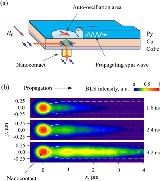
Figure 17. (a) Layout of the magnonic system enabling excitation of propagating spin waves by pure spin currents generated by the NLSI mechanism. Reproduced from [124]. CC BY 4.0. (b) Color-coded maps demonstrating excitation and propagation of a 3 ns long spin-wave pulse. Reprinted from [125], with the permission of AIP Publishing.
Download figure:
Standard image High-resolution imageWe used imaging of spin waves with sub-micrometer spatial resolution, enabled by micro-focus BLS spectroscopy [119], to show that this system is capable of generation of spin waves in a broad frequency range by the dc driving electric current (figure 17(b)). The generated spin waves exhibit a large decay length of several micrometers, facilitated by the relatively large thickness of the spin-wave guiding subsystem. Moreover, analysis of the power consumption showed that the power efficiency of these devices is superior to the magnonic systems that utilize traditional inductive spin-wave excitation using microwave currents generated by the external microwave sources. Additionally, the excitation mechanism was found to be intrinsically fast, which allows generation of ultra-short spin-wave packets with the duration of a few nanoseconds [125]. This possibility is particularly important for the implementation of high-speed magnonic circuits.
While NLSI-driven magnonic devices offer numerous benefits, they do not use some of the important advantages that are provided by pure spin currents. In particular, since these devices rely on the local current injection through a nano-contact, they do not allow one to use the same driving current for long-range enhancement of propagation of the generated spin waves, as was demonstrated for spin currents generated by SHE [120]. After an intensive search for a suitable geometry, in [126], we demonstrated an SHE-driven system enabling excitation of spin waves, and simultaneous enhancement of their propagation by pure spin currents. The system utilized a new concept of nano-notch SHE oscillators directly incorporated into a magnonic nano-waveguide. These devices (figure 18(a)) were based on 180 nm-wide nano-waveguides patterned from a Py (15 nm)/Pt (4 nm) bilayer. Ion milling was used to pattern a rectangular 200 nm-wide and 10 nm-deep notch in the top Py layer of the waveguide. When electric current I flows through the device, SHE in Pt injects pure spin current IS into the Py layer, producing anti-damping spin torque. The thickness-averaged magnitude of this torque is inversely proportional to the thickness of the magnetic layer. Thus, the effects of spin torque on the 5 nm-thick Py layer in the nano-notch area are significantly larger than on the 15 nm-thick Py waveguide. As the current I is increased, damping becomes completely compensated in the nano-notch region, resulting in the local excitation of magnetization auto-oscillations serving as a source of propagating spin waves. Simultaneously, the damping is only partially compensated in the rest of the waveguide, resulting in the enhancement of spin-wave propagation.

Figure 18. (a) Schematic of the SHE-driven device based on the notched Pt/Py bilayer nano-waveguide. (b) Color-coded spatial maps of spin-wave intensity. Dashed lines on the maps show the outlines of the waveguide and of the nano-notch. [126] John Wiley & Sons. [Copyright © 2018 WILEY‐VCH Verlag GmbH & Co. KGaA, Weinheim].
Download figure:
Standard image High-resolution imageMicro-focus BLS measurements showed that the auto-oscillations in the nano-notch can efficiently emit propagating spin waves into the waveguide (figure 18 (b)). This emission was found to be strongly unidirectional, with the preferential direction controlled by the direction of the static magnetic field. Additionally, it was shown that the propagation length of emitted spin waves is enhanced by up to a factor of three by the spin current injected over the entire length of the waveguide. Therefore, this system combines all the advantages provided by spin currents to locally excite propagating spin waves, and to simultaneously enhance their propagation characteristics. Additionally, the proposed approach can be easily scaled to chains of SHE nano-oscillators coupled via propagating spin waves, facilitating the development of novel nanoscale signal processing circuits such as logic and neuromorphic computing networks.
10.2. Current and future challenges
One of the main challenges in the ongoing development of spin current-driven magnonics is associated with the nonlinear phenomena stimulated by pure spin currents, which drastically limit the operational regimes and device geometries, as well as the possibilities for device integration. In particular, nonlinear scattering of propagating spin waves from magnetic fluctuations enhanced by pure spin current has been identified as the main mechanism responsible for the saturation of the anti-damping effect, which has so far prevented the development of devices where the propagation losses of spin waves are completely compensated [120], and has imposed strict limitations on the spin current-driven nano-oscillator geometries [122]. Additionally, the nonlinear frequency shift of large-amplitude current-induced auto-oscillations is known to be responsible for the spatial self-localization of oscillations, preventing the emission of propagating spin waves [122]. Recently, it was shown that these limitations can be overcome by using materials with PMA. PMA controls the nonlinear frequency shift, allowing one to design systems where self-localization is avoided [127, 128]. Additionally, it was recently shown that by tailoring the PMA strength, one can suppress the nonlinear scattering [129], which can open the possibility to achieve decay-free propagation of spin waves, and perhaps even their true amplification. This approach is particularly promising thanks to the recent progress in the fabrication of nanometer-thick low-damping YIG films with PMA, which has already enabled highly efficient current-driven generation of coherent propagating spin waves in this archetypal low-loss magnetic insulator [127].
10.3. Concluding remarks
Pure spin currents offer novel opportunities for the development of nano-magnonics, and provide the means to address the main challenges associated with the downscaling of magnonic devices, their performance enhancement and integration. We expect that spin currents will be essential to making magnonic nano-systems a competitive alternative to conventional CMOS-based microelectronics.
Acknowledgments
This work was supported in part by the Deutsche Forschungsgemeinschaft (Project No. 423113162) and the NSF Grant No. ECCS-1804198.
11. Interaction of magnons with spin textures
Edoardo Albisetti1, Daniela Petti1, Riccardo Bertacco1, Helmut Schultheiss2,3
1Polytechnic University of Milan, Italy
2Helmholtz-Center Dresden–Rossendorf, Institute of Ion Beam Physics and Materials Research, Germany
3 Technische Universität Dresden, Germany
11.1. Status
Spin textures, such as domain walls, vortices and skyrmions, are nonuniform configurations in the arrangement of spins in magnetic materials, which are raising interest as active components in data storage and signal processing. One of the most relevant key features, which makes spin textures so appealing, is the fact that they combine stability and resilience with a remarkable degree of tunability and scalability toward nanoscale dimensions. Such features can be the basis for developing new device concepts where the properties and dimensionality of the spin textures ultimately determine the device functionality and scalability. Notable examples of applications are represented by magnetic vortex oscillators, which exploit the GHz dynamics of nanoscale magnetic vortices for emitting RF signals when excited by a dc current, or racetrack memories, where domain walls or skyrmions representing magnetic bits are electrically created, displaced and detected within magnetic nanowires. Recently, the possibility of harnessing the potential of spin textures in the field of magnonics has sparkled a new wave of theoretical and experimental efforts, aiming to study the rich phenomenology of the interaction of spin waves with spin textures, to demonstrate new device concepts, or to ultimately overcome some of the long-standing challenges of the field.
11.2. Current and future challenges
One of such challenges is the efficient spatial confinement and waveguiding in 2D circuits. The conventional method, based on geometrically patterning magnetic micro or nanoconduits, has important limitations as it is hardly scalable and not suitable to realize complex spin configurations. For this purpose, the use of spin textures such as magnetic domain walls and tailored domain structures represents a promising avenue (see figure 19). In [80] it was proposed that domain walls in ultrathin films act as magnonic nano-waveguides, supporting confined modes, called Winter magnons, which are not present in the bulk of the film, and which can be guided in curved geometries. The spin-wave channelling within domain walls was demonstrated experimentally in in-plane magnetized films featuring 180° Néel domain walls, where spin waves were excited by using an oscillating RF magnetic field generated by a metallic stripline [130]. The spin-wave localization at the wall was demonstrated by acquiring the spatially-resolved map of the spin wave intensity via BLS, which showed the presence of low-frequency propagating modes, which are not supported by uniform domains.
Figure 19. (a) Simulated spin-wave channelling by means of curved domain walls. In the inset, a cross section of the spin configuration is shown. Reproduced from [80]. CC BY 4.0. (b) Spin-wave intensity measured across a domain wall for different externally applied magnetic fields highlighting the localization of spin waves within the domain wall and the tunability of the channel position. Reprinted by permission from Springer Nature Customer Service Centre GmbH: [Springer Nature] [Nature Nanotechnology] [130] (2016). (c) Experimental spin-wave spectra measured across nanopatterned stripe domains, showing strong spatial modulation of the spin-wave intensity. Reprinted by permission from Springer Nature Customer Service Centre GmbH: [Springer Nature] [Nature Nanotechnology] [131] (2016).
Download figure:
Standard image High-resolution imageTailored magnetic domains can be also used for spatially controlling the spin-wave excitation and propagation within continuous films. In [131], localized heating with a nanoscopic atomic force microscope tip was used for nanopatterning magnetic domains with tailored shape and magnetization direction in an exchange biased ferromagnetic thin film. This allowed both to spatially modulate the intensity of the spin waves and to select different propagating modes, by exploiting the anisotropic excitation efficiency and dispersion of spin waves with respect to the magnetization direction. Furthermore, the use of periodic arrays of narrow magnetic domains was proposed as the basis for building MCs with tunable bandgap.
One of the most appealing features of employing domains and domain walls as building blocks for magnonic devices is their reconfigurability. In fact, the volatile or non-volatile modulation of the spin textures via external stimuli allows the implementation of a dynamically reconfigurable functionality, such as the precise displacement of domain wall-based waveguides, the real-time modulation of the bandstructure in MCs, or the reversible control of the spin-wave transmission across domain walls [132].
A promising application which exploits these unique capabilities is the realization of reprogrammable spin-wave circuits where propagating spin waves are confined at the nanoscale, steered and let interfere in a controlled way. In [133], it is shown theoretically that it is possible to design a reprogrammable spin-wave circuitry providing unidirectional spin-wave transport using domain walls in presence of DMI. Experimentally, a prototypic nanoscale spin-wave circuit based on spin textures has been demonstrated using nanopatterned Néel domain walls, where the spatial superposition and interference of confined modes was controlled by reconfiguring the waveguides in real-time [24].
The dynamics of spin textures is also interesting for the generation of propagating, short-wavelength spin waves. In fact, as the wavelength approaches sub-micrometric dimension, conventional generation methods based on microstructured antennas become inefficient. Recently, it was demonstrated that magnetic vortex cores and domain walls emit spin waves when driven in oscillation around their equilibrium position by an RF magnetic field [134] (see figure 20(a)). Since the frequency and wavelength of the emitted spin waves can be easily tuned by controlling the excitation field, this method represents a promising avenue for developing highly flexible nanoscale spin-wave sources. In [113] this concept was used as basis for developing an optically-inspired platform, where magnonic nanoantennas based on domain walls and vortices allow for wavefront engineering, focusing, and interference of short-wavelength spin waves in SyAFs.

Figure 20. (a) Experimental x-ray microscopy imaging of the tunable emission of short-wavelength spin waves by vortex cores. Reprinted by permission from Springer Nature Customer Service Centre GmbH: [Springer Nature] [Nature Nanotechnology] [134] (2016). (b) Antiferromagnetic domain walls as spin wave polarizer and retarder. Reproduced from [137]. CC BY 4.0. (c) Proposal of topological magnonic circuitry based on the unidirectional propagation of topologically protected spin-wave modes along sample edges and domain walls. Reprinted (figure) with permission from [138], Copyright (2018) by the American Physical Society.
Download figure:
Standard image High-resolution imageTwo recent developments in the field of spin–orbit torques (SOT) opened the door to unify the generation-manipulation of spin textures and the excitations of magnons therein in a single device based on a simple bilayer of a HM and a ferromagnet. A dc current injected into such a bilayer proved not only to be an efficient method for initializing domain walls or skyrmions with well-defined chirality [135], but also to drive high frequency magnon auto-oscillations within nano-sized domain walls even in the absence of an externally applied magnetic field [136]. This renders spin textures a powerful nano-interface between electronics and magnonics.
11.3. Concluding remarks
A futuristic outlook on applications of spin textures for magnonics is featured by recent reports on simulations of magnon transport in antiferromagnets or more exotic systems such 2D ferromagnets. Antiferromagnets are appealing because they offer a new degree of freedom given by the magnon polarization, where domain walls can act as polarizing elements [137] (see figure 20(b)). Truly 2D ferromagnets offer great potential for magnonics due to protected, non-reciprocal edge states emerging from the topology of the magnonic band structure [138] (see figure 20(c)). These special magnonic states are the magnonic analogy to surface states in topological insulators and exist even in domain walls. Even though these examples are far from experimental realization they indicate the vast possibilities and phenomena still to be discovered and used in the field of magnonics.
Acknowledgments
Funding from the European Union's Horizon 2020 research and innovation program is gratefully acknowledged under Grant Agreements Number 705326, project SWING, and number 948225, project B3YOND. Financial support by the Deutsche Forschungsgemeinschaft is gratefully acknowledged within program SCHU2922/1-1.
12. Graded index magnonics
V V Kruglyak1 and V D Poimanov2
1University of Exeter, United Kingdom
2Donetsk National University, Ukraine
12.1. Status
The topic of wave excitation, propagation, and confinement in graded (i.e. continuously inhomogeneous) media arises naturally for any kind of waves, and spin waves are not an exception. The relevant part of spin wave research is known as 'graded index magnonics' [139]. Yet, the concept of a refractive index is not as useful in magnonics as it is e.g. in optics and acoustics. Indeed, thanks to the gapless, linear, and isotropic dispersion relations conventionally found for light and sound, the optical and acoustic refractive indices (defined as ratios of the wave speeds in the reference and graded media) hold for wide ranges of frequencies. In contrast, these properties of the dispersion relation are not usually found for spin waves, and so, the conventional definition of the refractive index has limited value in magnonics. Instead, we use term 'magnonic index' for a quantity that scales with the wave number that the spin wave of a given frequency acquires in a given point of space under assumption that it propagates in the same direction in a uniform medium with magnetic properties in that point and under equivalent conditions. The latter must include appropriate static and dynamic magnetic fields, such as the bias and demagnetising fields due to the sample's structure. Inevitably, the non-locality of the magneto-dipole interaction makes this (and in fact, any) definition of the refractive index for spin waves either limited or ambiguous. Yet, it is often useful in interpretation of experimental and numerical results and when adapting design recipes from e.g. graded index optics.
Schlömann was one of the first to exploit graded profiles of the magnonic index, pointing out that the non-uniform static internal magnetic field can mediate coupling between spin waves and essentially uniform (on the scale of the spin wave wavelength) dynamic magnetic fields [140]. This, now known as 'Schlömann' mechanism of spin wave excitation extends to effective magnetic fields of any origin, including not only static but also dynamic non-uniform demagnetising fields [141], inherent to patterned magnetic structures. Morgenthaler was one of the first to apply graded magnonic index to confine [142], to focus [143] and to steer [144] spin waves propagating in bulk YIG samples, which were also considered by Schlömann [140]. Most recently, similar ideas have been systematically developed to demonstrate spin wave confinement [145], focusing (figure 21 [146]) and steering (figure 22 [147]) by graded profiles of the magnonic index in thin film magnonic structures.

Figure 21. Numerically simulated snapshots of the dynamic magnetisation component mx in units of the saturation magnetisation are shown for a packet of forward volume magnetostatic spin waves propagating through a magnonic Luneburg lens (black circle) for time moments of (a) 16 ns, (b) 45 ns, (c) 80 ns, and (d) 106 ns after excitation. The graded magnonic index profile corresponding to the Luneburg lens is formed by a gradual local increase of the saturation magnetisation in an out-of-plane magnetised thin film of YIG. Reprinted from [146], with the permission of AIP Publishing.
Download figure:
Standard image High-resolution image
Figure 22. Effect of the anisotropy of the magnonic dispersion is illustrated for the case of spin wave propagation in an asymmetrically magnetised permalloy T-junction. (a) The calculated distributions of the static magnetisation (arrows) and the projection of the internal magnetic field onto the magnetisation (color scale) are shown for the magnetic field of H B = 500 Oe applied at 15° to the vertical symmetry axis. Each arrow represents the average over 5 × 5 mesh cells. (b) kx spectra of the dynamic magnetisation distributions across the leg (gray line in (a)) and along the arms (blue line in (a), amplified ×5) of the T-junction excited at 7.52 GHz are shown by the gray and blue curves, respectively. The kx value of 0.94 μm−1 indicated by a dashed line corresponds to maximum spin-wave Fourier amplitude. (c) A construction illustrating the extraction of the group velocities of the incident (index 'i') and reflected (index 'r') beams is shown for the white boxed pixel in (a). For the specific kx value of 0.94 μm−1 (which is indicated by the vertical dashed lines here and in panel (b)), the group velocities are perpendicular to the characteristic isofrequency curves (purple). The ky value is given by the crossing of the dashed line and the isofrequency curve. Here and in panel (b), the region shaded yellow has the same size and represents the range of forbidden kx values, as calculated for the white boxed pixel and for pixels on the gray line in (a), respectively. (d) The extracted directional unit vectors of the group velocities and wave vectors are shown for kx values shown by the vertical dashed lines in (b) and (c). Reprinted (figure) with permission from [147], Copyright (2015) by the American Physical Society.
Download figure:
Standard image High-resolution imageExperimentally, graded index magnonics has been the primary beneficiary from development of time-resolved imaging techniques [147]. Importantly, these were recently extended to spin waves with sub-micrometre wavelengths in low-damping YIG [148]. Theoretically, it has mostly benefitted from existing concepts and methods developed in and then adopted from other areas of physics. For instance, the analogy between the static internal field for exchange spin waves and the potential energy for a quantum-mechanical electron was exploited in references [140, 145] along with the Wentzel–Kramers–Brillouin (WKB) method (quasi-classical approximation). In reference [142], the latter was applied to purely magneto-dipole spin waves. The magnonic Luneburg lens shown in figure 21 [146] is designed using the principles from geometrical optics and ultimately classical mechanics. However, as in the case of the refractive index, such analogies have limited applicability. Hence, numerical micromagnetic simulations have been increasingly often used in graded index magnonics both as a stand-alone tool and as a part of hybrid theoretical analyses [141, 145–147].
Several factors will continue driving research in graded index magnonics in the foreseeable future. Firstly, various magnetic non-uniformities and the associated graded magnonic index are ubiquitous in realistic magnonic and more generally magnetic structures [139, 141, 145, 147], making studies and thorough understanding of the associated dynamics a necessity of high-frequency magnetism and spintronics. The same applies to magnonics, including nearly every topic in this review. Secondly, deliberately created graded magnoniclandscapes could enable some important yet elusive concepts from other areas of physics [146,149,150] to be tested in the laboratory. Finally, innovative graded magnonic profiles will prove indispensable in eventual practical magnonic devices, either broadening their functionalities or even underpinning new ones.
12.2. Current and future challenges
As no other sub-field of magnonics, experimental studies into graded index magnonics suffer from excessively high magnetic damping. The major challenge is then to learn to create designer magnonic landscapes in low damping magnonic materials. To illustrate this challenge, we consider the realisation of the magnonic Luneburg lens shown in figure 21
[146]. A 2 μm thick film of YIG is used as a magnonic medium in the micromagnetic model, and the required lens is created by modestly increasing the saturation magnetisation to the required profile. This increase would however be difficult to realise experimentally. Indeed, local ion implantation or heating would typically decrease (rather than increase) the magnetisation, while inevitably also increasing the damping. The use of miniaturised magnets to create a required bias field profile or Peltier elements to locally cool the film is probably possible but would obscure the optical access necessary for spin wave imaging. A graded decrease of the film thickness by a factor of  is an analytically exact solution of the problem [146] but would most likely be challenging technologically for YIG if we were to preserve its low damping.
The results shown in figure 21 were produced in the forward volume magnetostatic spin wave geometry. This geometry in itself is a significant practical limitation due to the need to magnetise the film to saturation normal to its plane. However, the use of magnonic media with in-plane magnetisation raises challenges associated with the anisotropy of the spin wave dispersion, as illustrated in figure 22 [147]. Due to the Schlömann mechanism of spin wave emission, a uniform microwave magnetic field leads to emission of spin waves from the T-junction of two permalloy stripes into the horizontal stripe. For a modest tilt of the in-plane bias magnetic field, the highly non-uniform distributions of the internal magnetic field and magnetisation (figure 22(a)) and the associated non-uniform distribution of the directions of the group velocity vector (figures 22 (b) and (c)) lead to steering of the spin wave beam into just one of the two branches of the T-junction (figure 22 (d)). Found as a surprise in reference [147], this perfect steering of the spin wave energy illustrates the opportunities that could emerge once we resolve this challenge of an anisotropic magnonic dispersion.
The goal of mastering the spin wave control in graded magnonic media urges us to search for a universal description of their magnonic properties. Indeed, we have already commented on the limitations associated with the use of the refractive index concept [146]. The analogy with the quantum-mechanical electron [140] is also feeble since the concept of the electronic potential breaks beyond the exchange approximation. Even in the exchange approximation, the concept is generally invalidated (as is the concept of the wave impedance) by the ellipticity of the magnetic precession and emergence of evanescent spin wave modes in inhomogeneous anisotropic magnetic media [151]. The concept of the local magnetic susceptibility has not been demonstrated beyond the problem of spin wave excitation [141], while suffering from the nonlocality of the magneto-dipole interaction, similarly to the refractive index concept and the WKB method for spin waves [142, 145]. The natural abundance of non-reciprocal magnonic phenomena presents even greater and more fundamental challenges for development of a universal formalism for graded index magnonics.
Even when used for approximate or qualitative analyses, theoretical concepts and methods of graded index magnonics need to be developed and applied systematically, so as to account for (rather than to avoid) peculiarities associated with physics of spin waves. This applies to more traditional studies of spin waves in permalloy [141, 145, 147] and YIG [140, 142–144, 146, 148, 150] media as well as to studies expanding the range of addressed phenomena to spin waves and hybrid magnetic excitations (e.g. magneto-acoustic waves and magnetic polaritons) in more exotic material systems. The graded index magnonics of antiferromagnetic media seems particularly challenging, both experimentally and theoretically. Even as far as permalloy and YIG samples are concerned, the physics of nonlinear spin waves in graded media (nonlinear graded index magnonics) is still at its infancy. The fusion of topics of graded magnonic index and MCs [150] and the use of metamaterial approaches to design the graded magnonic index both look very promising yet hinging on our ability to resolve the challenge of the magnetic damping. Finally, we note that the topic of spin waves in samples with non-uniform magnetisation (spin textures) lends itself readily to the field of graded index magnonics [151], see the relevant section of this review.
12.3. Concluding remarks
Among its sister-areas of wave physics, magnonics is arguably the most complex and challenging. These challenges culminate in both experimental and theoretical studies of spin waves propagating in inhomogeneous magnetic media—those of graded index magnonics. However, as shown above as well as in other sections of this review, there are also great rewards and rich opportunities for those who will rise to the challenges and master the physics of spin waves propagating in graded magnonic media.
Acknowledgments
The research leading to these results has received funding from the Engineering and Physical Sciences Research Council (EPSRC) of the United Kingdom under Grant No. EP/L015331/1 and from the European Union's Horizon 2020 research and innovation program under Marie Skłodowska-Curie Grant No. 644348 (MagIC).
13. Spin–orbit effects in magnonics
Anjan Barman1, Sourav Sahoo1 and Jaivardhan Sinha2
1S N Bose National Centre for Basic Sciences, India
2SRM Institute of Science and Technology, India
13.1. Status
Though the theoretical concepts of SOC and magnons were both formulated long time back, controlling and redesigning the exciting fields of magnonics and spintronics using SOC have drawn attention recently due to its various advantages [152, 153]. Emerging concepts related to the SOC effects are considered crucial for improving the performance of spin-based devices by markedly reducing the power consumption. The SOC effects can be primarily categorized into intrinsic and extrinsic phenomena. While the intrinsic SOC in simplified assumption can be imagined as a local magnetic field related to band structure, the extrinsic SOC is caused by defects and impurities which act as scattering centers [154, 155]. The intriguing phenomena, namely PMA, SHE, Rashba effect, spin pumping and DMI are all known to have origin in SOC [156–158]. In recent times, the experimentally realized SOT originating from pure spin current is expected to play crucial roles in controlling the magnetization as well as spin wave (SW). In comparison to conventional spin-transfer torque, utilizing SOT in magnonic devices is simple and dramatically more efficient. In SOT spin-polarization arises from the carrier velocity difference and a spin filter is not required to generate spin current. The ability of SOT to compensate Gilbert damping over extended regions has opened up a new avenue for on-chip SW communication devices [152, 153]. In order to develop ultrahigh-speed beyond–CMOS SW-based technology for signal processing, it is crucial to achieve long-range enhancement of SW propagation in a variety of magnonic devices. Development of integrated magnonic circuits requires enhanced SW coherence and propagation length. Both these can be addressed by utilizing SOT, which provides the ability to electrically control damping, resulting in significantly enhanced SW propagation. The complete compensation of damping allows coherent local SW generation. Furthermore, enhanced SW transmission can be achieved if the concept of SOT is integrated in the magnonic devices. SOT-driven SWs can be directly applicable to additional nonconventional computing schemes such as neuromorphic-based computing as well as next generation magnetic memory devices with almost unlimited endurance.
SW dispersion in magnonic antidot waveguides has been theoretically investigated in symmetric and asymmetric structures to understand the modification in magnonic band gaps [159]. The effects of intrinsic symmetry breaking factors were found to be compensable by careful adjustment of extrinsic factor. The underlying principle is based upon the translational and mirror symmetries associated with the crystal structure. Thus, the idea of correcting an intrinsic defect by extrinsic means needs experimental realization in MC developed using thin film heterostructures where ferromagnetic thin film layer is placed adjacent to large spin–orbit scattering centers. Further, two-dimensional antidot MCs carved in magnetic multilayers with PMA have shown localized and collective SW excitation, where sharp decrease of SW frequencies is driven by a dynamical coupling between the localized modes within the shells, caused by tunneling and exchange interactions [160]. The localized shell modes are efficiently tunable by antidot shape through the control of domain structure inside the shells [161].
Observation of chiral spin textures such as spin spirals, helices and skyrmions are mainly related to the stabilization of iDMI in thin film heterostructures where a ferromagnetic layer is placed adjacent to a HM layer or 2D material, e.g. graphene. Chiral MCs, where interplay of SW with DMI can be tailored, have been theoretically predicted to exhibit exceptional features, e.g. ability to transfer energy unidirectionally. Further, dynamical control of magnetic damping by SOT allows tunable control of SW propagation. To this end spin-charge conversion efficiency, namely, spin Hall angle (SHA) plays an important role. An unambiguous technique based on all-optical TR-MOKE have been implemented to estimate SHA in HM/ferromagnet bilayers along with deciphering the effect of spin current generated by SHE and spin pumping [156, 158].
On the other hand, influence of iDMI on the SW dispersion has become a topic of intense interest. The DMI-induced SW asymmetry has been theoretically predicted, which proposed an estimation of the strength of DMI by measuring the frequency difference of counter propagating SWs. In particular, by means of BLS, nonreciprocal SWs were observed in HM/ferromagnet thin film heterostructures [157]. The frequency asymmetry in the SW dispersion of counter propagating Damon–Eshbach (DE) SWs was confirmed in various combinations of heterostructures due to the presence of iDMI. Furthermore, it was also predicted that in systems with bulk DMI a frequency difference could be observed in the backward-volume geometry. Some of the chiral spin textures have manifested this effect [152].
13.2. Current and future challenges
The current and future challenges can be divided into two classes: (a) scientific challenges and (b) technical challenges. The overriding goal of the scientific challenges is to combine a number of spin–orbit effects with the MC and subsequently to the magnonic devices. For example, simultaneous existence of PMA and DMI as well as patterning of two-dimensional MC can help in stabilizing topological magnetic objects like skyrmions or merons and more efficient control of their dynamics. Development of one- and two-dimensional MCs on FM/NM heterostructures with iDMI will lead to novel magnonic band structures with the evolution of new bands and bandgaps due to the asymmetric DE SW dispersion in presence of iDMI (an example of SW dispersion in a one-dimensional magnetic antidot waveguide without and with DMI is shown in figures 23(a)–(c)).
Figure 23. (a) Simulated spin-wave dispersion curves for a one-dimensional Ni80Fe20 antidot waveguide with 3 μm length and other dimensions as shown in the schematic at the inset. The spin-wave dispersion is calculated in the DE geometry in presence of a bias magnetic field of 1.01 T. Further application of iDMI strength of (b) D = −2 mJ m−2 and (c) D = 2 mJ m−2 have dramatically modified the spin-wave dispersion curves. (d) Application of a current density of 1 × 10¹¹ A m−2 on (c) has reduced the spin-wave amplitude significantly. The color map of the spin-wave dispersion is jet, i.e. red corresponds to maximum and blue corresponds to minimum spin-wave amplitude.
Download figure:
Standard image High-resolution imageThe wave-number dependent skew scattering of magnons from skyrmions gives rise to the topological magnon Hall effect, while interaction of skyrmions with current flow leads to skymion Hall effect. However, a combined effect of current flow and magnon on skyrmions may lead to novel effects due to the competition between thermally-driven radial magnon current, transverse magnon current and electron flow. Scattering of magnons from a skyrmion lattice can open magnonic bandgap, leading toward dynamic MC, which can be continuously tuned by a dc magnetic field. One of the primary bottlenecks of magnonics is the large damping of SWs in metallic ferromagnets which limits the SW propagation distance and device efficiency. Antidamping properties of SOT may dramatically reduce damping, but it has not been investigated extensively in MCs. Spin current may be used globally or locally to selectively amplify or attenuate propagating SWs (an example is shown by numerical simulation in figure 23 (d), where SW amplitude has been dramatically reduced by application of spin current) leading toward development of magnon logic or transistor. Finally, controlled magnon auto-oscillation at zero magnetic field can lead to extremely energy-efficient magonic devices.
The technological challenges primarily concern about the fabrication of devices, precision measurements and their application. The advancement of devices hinges on the capability to downscale the individual circuit elements. A conceptual magnonic device in figure 24 shows the excitation can be done by various means such as microwave antenna, voltage controlled magnetic anisotropy, SOT by SHE or spin pumping, all of those throw challenges in downscaling the excitation element by keeping the relevant property intact. The fabrication of nanoscale MCs by electron-beam lithography or focused ion-beam milling on thin film heterostructures by keeping the spin–orbit effects intact is also a great challenge [160, 161] and extensive research is required to overcome this. To this end topological magnetic texture-based dynamic MC originated from spin–orbit effects could be a solution but controlling ordered arrays of such textures over large area would be challenging. The electrical detection based on inductive techniques or inverse SHE faces similar challenges. Alternative detections like optical, x-ray or electron microscope are useful but not viable for practical application. Furthermore, given the intriguing physics involved in the three-dimensional MCs, it will be important to understand the spin–orbit effects on magnons in such systems for their applications in magnonic devices.
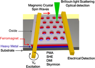
Figure 24. Schematic of a conceptual magnonic device composed of antidots on magnetic thin film heterostructures having different SOC related properties with electrical excitation and optical as well as electrical detection technique.
Download figure:
Standard image High-resolution image13.3. Concluding remarks
The ability to implement spin–orbit effects to modify the magnon properties in tailored magnetic materials holds the key for future energy-efficient high-frequency nanoelectronic devices. These will be the subject of future investigation from fundamental interests as the complexities involved needs further in-depth exploration using experimental and theoretical studies. We envision the possibility of new information processing devices in the future based on new classes of MC where spin–orbit effects will be crucial ingredients.
14. THz magnonics
Hyunsoo Yang1 and Markus Münzenberg2
1National University of Singapore, Singapore
2University of Greifswald, Germany
14.1. Status
Achieving a faster and most energy efficient data processing has been a major task in modern spintronics. To bring magnonics to THz frequency scale, we need three things: THz excitation, as an ultrafast signal input, THz frequency spin-excitations and THz detection of spin-wave signals. From early on, ultrafast spin-dynamics aimed to develop picosecond stimuli by using Auston switches or femtosecond laser pulses for excitation directly. In early ultrafast demagnetization in ferromagnets, the role of THz high-energy-spin waves on the 100 fs to ps time scales driven by infrared femtosecond lasers was clear. However, they could not be exploited so far to generate high energy spin waves in the THz frequency spectrum directly by the laser pulse heating. A breakthrough on THz stimuli was the generation of THz current and field pulses via laser driven picosecond charge and spin-currents. One such central scheme is to utilize spin to charge conversion. The possibility of laser-induced spin to charge conversion at THz frequency was first demonstrated in 2013 [162]. In ferromagnet (FM)/HM heterostructures, laser excitation lifts the electrons in the ferromagnet by the photon energy into different states in the spin-split band structure, thereby generating a non-equilibrium electron distribution. The laser-excited majority spin electrons have a mainly sp-like character and much higher velocity than the excited minority spin electrons with a d-type character. Subsequently, the diffusion of spin current toward the adjacent HM layer results in a charge current generation due to the spin to charge conversion effect such as the inverse spin Hall and inverse Rashba–Edelstein effects. The ultrafast transient charge current thus induces a THz electromagnetic radiation as schematically shown in figure 25(a). Three independent groups recently reported using optimized emitter structures that the intensity of the THz radiation competes with standard THz emitters [163–165]. The emitter spectrum of the spintronic THz emitter is compared to a commercial interdigitated GaAs switch and a ZnTe emitter. The bandwidth is much larger covering the low frequency (0.1–3 THz) as well as high frequency up to 30 THz without any gap. This indicates that at the same time shorter current pulses, with ultrafast rise times of ∼0.1 ps can be generated. Such spin-based THz emitters are insensitive to the polarization and helicity of an incident laser beam which indicates the noise resistive feature. In contrast, the amplitude and polarization of THz waves are fully controllable by an external magnetic field. Spin-based THz emitters can be fabricated on flexible substrates, and driven by a fiber based low power laser [164]. Together with the low cost and mass productive sputtering growth method for the magnetic heterostructure stacks, the spin-based THz emitters can be readily applied to a wide range of THz applications. This opens up a route not only to novel THz emitters, but also potential spintronic devices manipulating spin current bursts on a THz timescale.
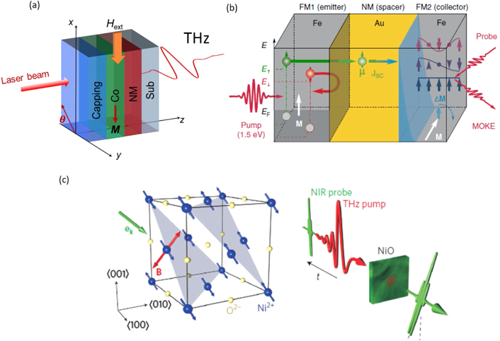
Figure 25. (a) A typical ferromagnet (FM)/non-magnet (NM) sample structure and the THz emission geometry. The femtosecond laser beam is used for pumping the sample. The external magnetic field (Hext) is along the x-axis. In (b) and (c) two strategies are shown to excite spin waves using THz pulses in the THz frequency range. (b) Laser-induced excitation of spin dynamics via spin currents pulses. Due to the spatial confinement of the STT perturbation (blue shaded area), spin waves with a broad spectrum of nonzero wavevectors are excited and can be probed by the MOKE in the collector. The exchange standing spin waves are confined in nanometer thick layer, where the frequency increase as ∼k2. Reproduced from [165]. CC BY 4.0. (c) Crystal lattice of NiO with antiferromagnetically ordered spins (blue arrows) in the (111) planes (light blue) and the direction of the THz magnetic field B (double-ended red arrow). An intense free-space THz interacts with the electron spins of a sample to launch a coherent magnon wave. Here the intrinsic modes are in the THz frequency range. A femtosecond near-infrared (NIR) probe pulse (green curves) measures the induced net magnetization by the Faraday effect. Reprinted by permission from Springer Nature Customer Service Centre GmbH: [Springer Nature] [Nature Photonics] [165] (2011).
Download figure:
Standard image High-resolution imageIt was demonstrated that THz spin waves can be directly excited by the laser driven spin-polarized current pulses in Fe/Au/Fe multilayers [166]. The authors have shown that standing spin wave modes can be excited in a 15 nm thick Fe film due to ultrashort laser-induced spin current bunches as shown in figure 25 (b). Laser pump pulse impinging on the first Fe layer (emitter) excites hot electrons at elevated energies. Due to the unequal transmittance of the Fe/Au interface for the majority (green) and minority (red) hot electrons, spin polarized hot electrons are emitted into Au. The spin polarized electrons reach the second ferromagnet (FM2) ballistically and the injected spin current absorbed on a length scale of well below 2 nm allows an asymmetric spin dynamics excitation due to the spin transfer torque effect. Here spin waves for 0.1–0.6 THz are excited and probed by the Kerr rotation. Those THz spin-wave generators could be used to inject THz frequency spin waves into magnonic structures and devices in the future. This is an important step toward increasing the speed and miniaturization of the device size for possible magnonic applications. In the following we will discuss and compare the three ways THz frequency spin-excitations in magnetically ordered system: (i) homogeneous Kittel modes k = 0 excited off resonant, in large applied or internal anisotropy fields, (ii) spin waves with k ≠ 0 with strong exchange fields, found for standing spin waves and (iii) strong exchange fields in antiferromagnets and ferrimagnets.
For ferromagnetic systems, typical spin dynamics is in the GHz range which increases with the applied magnetic field. Resonances of the Kittel modes may reach THz frequencies with 20 T, posing a serious challenge without special high field facilities. However, if strong internal fields are generated by a high anisotropy or the exchange-interaction, one can reach the THz frequency branches of the spin-wave dispersion. In case of ferromagnetic systems, the strategy can be to decrease the spacing of a MC or waveguide to the ∼nm length scale and thereby to increase the k wave-vector to ∼2π/nm, since the dispersion increase with ∼k2, which is clearly challenging. However, one may reach >100 GHz by using self-organization, domain walls or networks, skyrmion lattices of nanometer periodicity and full or hollow nanowires. In case of antiferromagnetic systems, the exchange interaction to the neighboring spin of opposite orientation results in a very strong exchange field which can be up to 100 T. Thus in antiferromagnetic and ferrimagnetic systems, intrinsic natural frequencies of the spin-waves modes are in the THz range. Because of their insulating character and thus the absence of conduction electrons, oxides generally have very low damping. THz excitation of antiferromagnets by THz field pulses has been demonstrated in NiO and different orthoferrites XFeO3 (X = Nd, Pr, Y, Dy, Er, and Ho). The phase control of the exciting magnetic field pulse with THz frequency allows a coherent excitation and thus a phase control of the excited spin-wave as shown in figure 25 (c) [167]. Current status and perspectives focused on the THz antiferromagnetic dynamics and magnonics are discussed in detail in the next section on 'antiferromagnetic magnonics' (section 15). Not much is known about the propagation of THz spin-wave so far. Generally, the challenge is that high frequency spin-waves are considerably damped since the intrinsic dissipation (viscous damping) results in first order, a signal decay proportional to ∼1/ω. The above examples show how to generate THz spin currents or THz spin dynamics which can be utilized as input channels for THz magnonics.
14.2. Current and future challenges
The writing speed of ferromagnets has a physical limit in the GHz range due to their inherent slower magnetization dynamics, of the coherent switching of the Kittel mode or linear switching, connected to a thermal quenching. Antiferromagnets and ferrimagnets with antiparallel exchange coupling exhibit faster spin dynamics and could potentially overcome these limitations. Recently, it has been shown that not only femtosecond laser pulses, but also intense THz pulses can manipulate the magnetization, which could be a more energy efficient and fast way of controlling the magnetization. Within one picosecond, intense free space THz pulses abruptly change the magnetic anisotropy in antiferromagnetic TmFeO3 at 83 K, causing a full and coherent large angle (180°) switching, beyond small angle excitations, as shown in figure 26 (a) [168]. The switchable states can be selected by an external magnetic bias. The authors also showed that the low dissipation and the antenna's subwavelength spatial definition could facilitate scalable spin devices operating at THz rates. In a different report of figure 26(b), spin-transfer torques mediated by THz-driven electric fields (∼3 × 10⁹ A cm−2) have induced switching of antiferromagnetic domains in CuMnAs, a prototypical antiferromagnet at room temperature [169]. In addition, the multilevel neuron-like characteristics allow the integration of memory and logic within the antiferromagnetic bit cell. However, detecting the magnetization of antiferromagnets is challenging. In particular, the readout signal obtained from 90° rotation of above antiferromagnets via anisotropic magnetoresistance is not sufficient for fast reading and is not fully compatible with a MTJ based scheme. Although the device can be switched using a picosecond pulse input, the pulse duration does not necessarily correspond to the real switching time. Therefore, the temporal switching profiles need to be confirmed by time resolved measurements in order to evaluate the real switching speed of the device.
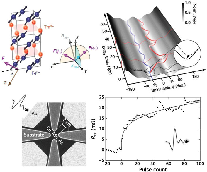
Figure 26. (a) Spin and lattice structure of TmFeO3. The ferromagnetic moment (F), antiferromagnetic vector (G), wave vector of the probe pulse (kNIR), and external magnetic field (Bext) are shown. On THz excitation, the magnetic potential W(φ) is abruptly modified. For a THz near field of E = 10 MV cm−1, the spins can be switched coherently by a single free space THz pulse (red trajectory) at φ1 ∼ φ0 + 90°. Reprinted by permission from Springer Nature Customer Service Centre GmbH: [Springer Nature] [Nature] [167] (2019). (b) CuMnAs device image. The multilevel memory signal as a function of the number of applied picosecond free space THz pulses. Reproduced from [168]. CC BY 4.0.
Download figure:
Standard image High-resolution imageBoth the effect of picosecond charge current pulses and the effect of ultrafast heating on the magnetization can be combined to build a THz magnetic memory. It was demonstrated in a ferrimagnetic material GdFeCo that a laser pulse application to the Austin switch generates a single sub-10 ps electrical pulse, which rapidly excites conduction electrons in magnetic metals [170]. This material is known to show magnetization reversal by a linearly polarized laser heat pulse that acts as an ultrafast heating stimulus. Here the current pulse generated by the Austin switch is directly injected into the GdFeCo with current densities of ∼109 A cm−2 and a pulse length below 9 ps. This pulse current injection into the smaller cross section and higher resistive GdFeCo element results in a deterministic switching event, measured by the magneto-optical contrast changing. The above examples show how THz inputs can excite spin dynamics by a small angle and even manipulate the magnetization by a full coherent 180° switching, which builds the basis of a THz magnonics concept.
The emitted THz waves from magnetic heterostructures not only show the potential as THz emitters, but also help to characterize various materials beyond conventional ones, such as ferrimagnets, 2D materials, topological insulators, and Weyl semimetal. The electrical spin torque, involving moving charges, suffers from unavoidable Joule heat and corresponding power dissipation, as well as a short spin propagation length. These fundamental obstacles can be overcome by the magnon torque [171]. In the future, the magnon current driven by all-electronic on-chip THz sources without a fs laser may enable novel spin memories operating at THz clock with least energy dissipation.
Acknowledgments
Please include any acknowledgments and funding information as appropriate. The work is supported partially by A*STAR AME-IRG (Grant No. A1983c0037), NUS Hybrid-Integrated Flexible (Stretchable) Electronic Systems Program, SpOT-LITE program (A*STAR Grant, A18A6b0057) through RIE2020 funds, the Deutsche Forschungsgemeinschaft (DFG), Priority Program 'Topological Insulators: Materials–Fundamental Properties–Devices SPP 1666' and Priority Program 'Skyrmionics Topological Spin Phenomena in Real-Space for Applications SPP 3137'.
15. Antiferromagnetic magnonics
Takahiro Moriyama1,2 and Shigemi Mizukami2,3
1Kyoto University, Japan
2Centre for Spintronics Research Network, Japan
3Tohoku University, Japan
15.1. Status
Antiferromagnets have multiple magnetic sublattices and the magnetic moments on the sublattices are compensated by each other. Negligible net magnetization, small magnetic susceptibility, and ultrafast magnetization dynamics are key characteristics of antiferromagnets [172] and are considered fruitful in the field of emerging antiferromagnetic spintronics [173]. Recent active studies have led to various interesting discoveries on interactions between the spin transport and the spin dynamics in antiferromagnets, which could make them alternative to the ferromagnets conventionally used in the present spintronics. Yet, there are still many open issues especially on the ultrafast magnetization dynamics in both physics and technological viewpoints which potentially fascinates the magnonics at the THz frequency leading to novel applications in information processing and tele-communications [174].
In the context of antiferromagnetic spintronics, the antiferromagnetic magnetization dynamics has recently been revisited long after early studies caught on in the late 50s by Kittel and others. Since there are more than one magnetic sublattices, multiple dynamic modes are generally observed. The eigenfrequency of the uniform resonance mode with the wavenumber k = 0 can be written by  where γ is the gyromagnetic ratio, HE is an exchange field, and HA is a uniaxial anisotropy field. Since HE, typically ∼1000 T, comes into play in the eigenfrequency, the antiferromagnetic resonance occurs at much higher frequency, i.e. ∼THz, than the FMR, typically ∼GHz. For the simplest case of a collinear easy-axis antiferromagnet with two magnetic sublattices, the dynamics is degenerated by two modes with opposite circular polarizations as illustrated in figure 27, which is in contrast to the ferromagnetic cases where only the right-handed mode is allowed. This is also true for non-uniform modes, or magnons with k ≠ 0, which are relevant to the magnonics. Therefore, comparing to the ferromagnetic cases, the antiferromagnetic magnons possess the additional freedom, i.e. the polarization, which is advantageous for information processing [175].
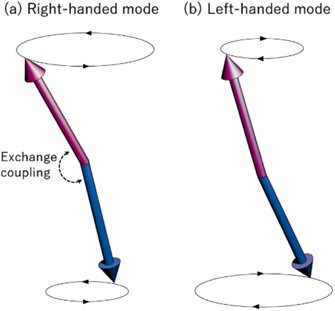
Figure 27. (a) The right-handed mode and (b) the left-handed mode of the antiferromagnetic dynamics.
Download figure:
Standard image High-resolution imageIn the early stage of the investigation, the state-of-art spectroscopy with a rather inefficient and weak far-infrared source was employed to investigate various antiferromagnets, such as NiO, CoO, MnO, Fe2O3, and Cr2O3. Although their high resonant frequencies have been experimentally confirmed, the experimental technique at the time was not sufficiently sensitive to capture more detailed dynamic properties such as relaxation mechanisms, e.g. magnetic damping, and the spatially non-uniform modes. Today, researchers take various experimental approaches for investigating the antiferromagnetic dynamics using more advanced measurement techniques such as the ultrafast measurement techniques with laser optics and THz spectroscopies with much better sensitivity. Due to some difficulties still lying on the measurements for antiferromagnets, materialistic approaches using pseudo-antiferromagnets, such as SyAFs (figure 28(a)) and rare-earth transition-metal (RE–TM) ferrimagnets (figure 28(b)), rather than using genuine antiferromagnets (figure 28(c)) are also in progress.
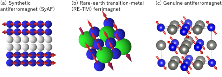
Figure 28. Schematic illustrations of (a) SyAF, (b) RE–TM ferrimagnet, and (c) genuine antiferromagnet, e.g. NiO.
Download figure:
Standard image High-resolution imageSyAFs typically consist of two ferromagnetic layers coupled antiferromagnetically via a non-magnetic insertion layer by the Ruderman–Kittel–Kasuya–Yoshida (RKKY) or magnetic dipole interactions. Since the strength of the antiferromagnetic coupling interaction (typically ∼1 T) is far smaller than that of genuine antiferromagnets and is tunable by adjusting the insertion layer thickness, the resonant frequency can be in the GHz range where the conventional microwave technology is applicable for measurements. Therefore, SyAFs are a good and easy testbed for investigating antiferromagnetic dynamics. One can observe a clear cross-over between the ferromagnetic dynamics and antiferromagnetic dynamics, the so-called acoustic and optic modes. Those show strong non-reciprocity in their propagations [176]. The relaxation of these modes and the dynamic coupling of them have been investigated in detail [177]. The mode amplification due to their non-linear coupling was also reported [178]. However, one must be cautious if the knowledge can necessarily extrapolate to genuine antiferromagnets, since most of the cases treat SyAFs as the two macro-spins coupled antiferromagnetically, which completely differs from genuine antiferromagnets where spins are atomistically coupled.
Another approach is taken by using RE–TM ferrimagnets having both magnetization and angular momentum compensation. RE is typically Gd or Tb and TM is Fe, Co, or their alloy. Due to the slightly different gyromagnetic ratios and their temperature dependences for the RE and TM, these ferrimagnetic alloys exhibit the magnetization and the angular momentum compensation at different temperatures. The intriguing magnetization dynamics emerges at the angular momentum compensation point but not at the magnetization compensation point which seems intuitively relevant to the antiferromagnetism. Because the magnetization dynamics are intrinsically governed by the angular momentum not the magnetic moment, they actually exhibit the antiferromagnetic dynamics at the angular momentum compensation point. The virtue of the RE–TM ferrimagnets is that one can easily access the antiferromagnetic dynamics while the magnetic susceptibility is non-zero, i.e. the static magnetizations are manipulable by external magnetic field. RE–TM ferrimagnets have been a testbed for the laser induced ultra-fast spin switching and ultra-fast DW dynamics [179].
Genuine antiferromagnets are yet the most interesting materials in antiferromagnetic magnonics. Material choices are tremendous ranging from insulators to metals. However, the measurement methodology is always a problem with these materials due to invisible nature of magnetization as well as the quite high resonant frequency. Nickel oxide is one of the most investigated materials since the old age. Recent revisits have revealed the detail magnetization dynamics in both time domain and broad band frequency domain, mostly focused on the localized dynamics with k = 0, using advanced technologies [180, 181]. Detail explorations of the antiferromagnetic dynamics, such as relaxation dynamics, magnetic damping, and Q-factors have recently revisited and progressed in accordance with theoretical developments [182]. So far, these ultra-high frequency spectroscopies are limited to bulk materials due mostly to the sensitivity issues. Investigation for antiferromagnetic thin films which are most relevant to the spintronic applications has not yet resolved.
15.2. Current and future challenges
Frontiers of the antiferromagnetic magnonics are in various directions. While the most important and impactful part of the antiferromagnetic magnonics is the use of genuine antiferromagents with the ultra-high frequency, materialistic approaches are still alternative to harness the gaps of the antiferromagnetic measurement techniques. Those materialistic approaches discussed above could of course find their own magnonic applications. However, for understanding the physics of magnons in genuine antiferromagnets, one should not rely too much on these approaches as it is still controversial whether those physics can be simply extrapolated.
In genuine antiferromagnets, comparing to the understanding of the resonant frequency ( ), magnetic relaxation mechanisms in antiferromagnets, such as magnetic damping which is typically evaluated from the spectral linewidth of the resonance, have not been investigate or discussed as much as the ferromagnetic cases. In the context of antiferromagnetic spintronics, revisits to the magnetic damping in antiferromagnet and to both experimental and theoretical investigations have recently been active [180, 181]. In both physics and engineering points of views, it is quite important to have a firm foundation of the relaxation mechanisms.
Direct observation of the antiferromagnetic magnon modes (k ≠ 0) is one of the most challenging business. Short wavelength and high frequency magnon modes inherent to the antiferromagnetic dynamics make those measurements quite difficult. Alternatively, although it is indirect observation, we should pay attention to the recent progress in the magnon spin current transport experiments where the spin current is carried through the antiferromagnets in the form of magnons [183].
So far, most of the investigations have been made with bulk antiferromagnetic materials and not much have been investigated in thin films, their multilayers, and confined structures where more interesting physics and applications should be found. It is interesting to see how the magnons behave in the confined structures which should be quite important for magnonic circuitry applications.
Finally, it is greatly desirable to push forward the development of antiferromagnetic measurement techniques. It is necessary to further increase the sensitivity of the THz spectroscopy to be able to measure the antiferromagnetic thin films. Magnetic imaging techniques using various probes such as magneto-optic effects and x-ray linear dichroism with photo electron emission microscopy are viable solutions. Very recent reports of the antiferromagnetic spin pumping effect could provide a unique perspective for electrical detection of antiferromagnetic dynamics [96, 184]. Advancements of these measurement techniques are certainly the key to progress the antiferromagnetic magnonics.
15.3. Concluding remarks
Antiferromagnetic magnonics is one of the most interesting destinations in recently emerging antiferromagnetic spintronics. The THz frequency and the polarization degree of freedoms certainly fascinate the conventional magnonic technologies and potentially yield novel applications in information processing and tele-communications. However, actual rise of antiferromagnetic magnonics has yet to come as the methodological challenges impede some of the key experimental studies. Further efforts in advancing the measurement technologies for antiferromagnets will open up tremendous opportunities in antiferromagnetic magnonics.
Acknowledgments
We thank to the Spintronics Research Network of Japan.
16. Spin-wave nonreciprocity
Pedro Landeros1,2, Rodolfo A Gallardo1,2, and Giovanni Carlotti3,4
1Universidad Técnica Federico Santa María, Chile
2Center for the Development of Nanoscience and Nanotechnology (CEDENNA), Chile
3University of Perugia, Italy
4CNR Instituto Nanoscienze, Italy
16.1. Status
Nonreciprocal propagation of electromagnetic, acoustic or spin waves is attracting more and more interest, due to the possible exploitation in devices for information and communication technology, such as isolators, circulators, phase shifter, etc. Nonreciprocity refers to the case where wave propagation changes, or it is even forbidden, upon inversion of the propagation direction and requires a breaking of the time-reversal symmetry [185]. This can be induced, for instance, by an applied stimulus, such as an external field with a specific bias direction, or by the presence of a substrate providing a suitable interaction. In the case of spin waves, nonreciprocity has been known to appear in different kinds of magnetic systems, leading to differences in either amplitude localization or frequency (the latter may also correspond to different velocity or phase, depending on the situation) for counter-propagating waves. Then, further advances in the field of nonreciprocal magnetic materials is of great scientific importance, since it will provide the technological basis for the realization of nanoscale nonreciprocal devices operating at microwave frequencies, and at the same time it will help us to solve the riddle of the relevance of the different fundamental physical interactions in magnetism.
The most well-known case of spin-wave nonreciprocity is the magnetostatic surface spin wave (DE wave), where the in-plane wavevector k is always perpendicular to the in-plane magnetization M. In a semi-infinite medium, such surface wave has an amplitude that decays exponentially within the medium and can travel from left to right but not in the opposite direction, thanks to the symmetry breaking introduced by the presence of the surface and the dynamic magnetostatic field. In the case of a ferromagnetic film with finite thickness d, the same physical mechanism leads to a nonreciprocity in the amplitude for magnetostatic waves if kd ≫ 1 (that corresponds, for spin waves with wavelength in the range of hundreds of nanometers, to film thickness well above one micron). In fact, the dynamic magnetostatic field localizes mostly in the upper or lower surface, depending on the relative orientation between k and M, as illustrated in figure 29 (top panel). For kd ≈ 1 (i.e. film thickness in the tens of nanometers range), instead, the DE hybridizes with discrete dipole-exchange spin wave modes, and there is still a preferential localization at either the upper or the lower interface. In the ultrathin film limit (kd ≪ 1), this behavior disappears, since the magnetostatic field and the wave amplitude are practically uniform across the film thickness.

Figure 29. Top panel: nonreciprocal spin wave propagation in the DE geometry (k ⊥ M) in a film with thickness d comparable to the spin-wave wavelength. It is seen that the wave amplitude is maximum at the bottom (top) interface for propagation along +x (−x). Central and bottom panels: nonreciprocal spin wave propagation in an ultrathin ferromagnetic film (FM), whose thickness is much lower than the spin-wave wavelength, in presence of a heavy-metal substrate (HM) that induces DMI. Spin waves propagating along +x and −x have opposite chirality and therefore different frequencies.
Download figure:
Standard image High-resolution imageIn addition to the above amplitude nonreciprocity, if there are different surface anisotropies Ks at the two faces of a film [186], then it can be also observed a frequency nonreciprocity, i.e. a small frequency difference Δf between two counter-propagating waves that is linear with ΔKs. An explicit formula for Δf was derived by Gladii et al (see equation (7) in [186]), showing that the frequency difference is linear with the wavenumber k at small film thickness, and predicting a more complex behavior for larger d. Note that such a nonreciprocity in frequency implies a phase-difference for waves covering the same distance in opposite directions.
Another source of both frequency and amplitude nonreciprocity in a magnetic film, which has been widely investigated in the last years, is the bulk or iDMI (see figure 29 , central and bottom panels). Experimental evidence, based on BLS measurements, of such a frequency difference due to DMI between counter-propagating spin waves was first reported by Di et al [187]. Shortly after, using the same technique in ferromagnetic/HM interfaces (such as, for instance, Co/Pt), several groups have measured a noticeable frequency asymmetry in the spin-wave dispersion, that is proportional to both the wavenumber k and the strength of the DMI constant D, in agreement with the expression [188]:
where ϕk
is the angle between k and M and γ the gyromagnetic ratio. These experiments allow to estimate D, whose measured values were collected in tables 5.2-3 of reference [188], which also contain, for the sake of comparison, measurements of D obtained with other techniques. It is now well established that the strength of the DMI is larger for interfacial systems than for chiral lattice ferromagnets with bulk DMI and that its strength decreases with the thickness of the ferromagnetic layer, while slightly increases with the thickness of the heavy-metal layer. Therefore, besides the enlargement of damping produced by the heavy-metal, a drawback of iDMI systems is that ferromagnetic layers with very low thickness d are needed (typically in the range between 0.5 and 5 nm) to generate a noticeable nonreciprocity, since D ∼ 1/d. For bulk DMI systems, such as the chiral lattice ferromagnet with tetragonal symmetry Cu2OSeO3,  , so the effect is maximum when it is measured for the backward-volume wave configuration (ϕk
= 0) [189]. If the magnetization is tipped out an angle α from the plane, a factor cos α enters in Δf for both bulk and interface DMI systems [188].
, so the effect is maximum when it is measured for the backward-volume wave configuration (ϕk
= 0) [189]. If the magnetization is tipped out an angle α from the plane, a factor cos α enters in Δf for both bulk and interface DMI systems [188].
A third case of spin-wave nonreciprocity, both in amplitude and in frequency, occurs if one considers two oppositely magnetized ferromagnetic layers, separated by a non-magnetic spacer [113, 190], shown in figure 30. In this case, the frequency difference is due to the dynamic volumetric and surface dipolar interactions. For a particular system with two identical layers of thickness d, separated by a non-magnetic layer of thickness s, the frequency nonreciprocity is given by equation (8) in reference [190]:
Figure 30. Top panel: sketch of the dynamic stray fields induced by the surface and volumetric dynamic magnetic charges in a ferromagnetic bilayer with antiparallel magnetizations, similar to that studied in reference [190], where spin waves propagate in the DE configuration. The large arrows depict the orientation of the dynamic magnetization, while the static magnetizations point along the ±z directions. The distributions of dynamic magnetizations and stray fields (curved arrows) are shown for both k > 0 and k < 0. Center panel: dispersion curves for spin waves propagating in a magnetic bilayer with antiparallel magnetization similar to that studied in reference [113]. It can be seen that, while the dispersion curve is symmetric around the k = 0 vertical axis for the magnetostatic backward configuration (ϕk = 0°), in the DE configuration (ϕk = 90°) the curves account for a marked nonreciprocity. In particular, in the frequency range (shaded area) between f0 and fmin, only waves with k > 0 can exist in the structure. Bottom panel: the above unidirectional propagation is illustrated by three snapshots (top view) of the simulation relative to different times for a spin-wave packet excited in the DE configuration, before and after reaching a 200 nm wide non-magnetic circular defect: no back-reflection is observed, since the counter-propagation is not allowed by the dispersion curve. Scale bars: 500 nm. (Latter panel) [113] John Wiley & Sons. [Copyright © 2020 WILEY‐VCH Verlag GmbH & Co. KGaA, Weinheim].
Download figure:
Standard image High-resolution imageThis frequency difference presents a non-monotonic behavior with k and d, with a well-defined maximum that is obtained for a value of k such that: ![$\mathrm{tanh}\left(kd/2\right)=kd/\left[1+k\left(d+s\right)\right]$](https://content.cld.iop.org/journals/0953-8984/33/41/413001/revision6/cmabec1aieqn6.gif) . Then, given d and s, the wavenumber k at which Δf is maximum can be easily estimated and one can easily verify that the effect is sizable in a very wide range of kd, i.e. for film thickness ranging from a few nanometers to several microns. Recent BLS measurements in a CoFeB (5.7 nm)/Ir (0.6 nm)/NiFe (6.7 nm) bilayer give Δf about 1–2 GHz [190], in agreement with theory. These values are comparable with typical ones for iDMI systems. Nonetheless, from the above formula for Δf, even larger values are found if the thickness d is increased, as in the recent study of CoFeB (45 nm)/Ru (0.6 nm)/CoFeB (45 nm) [113]. Remarkably, the frequency nonreciprocity can be turned off by changing the relative magnetic orientation from antiparallel to parallel alignment, i.e. just by simple switching, without any rotation of the field, as it is required in the case of DMI systems. Moreover, when the frequency of excitation is lower than f(k = 0), but larger than the low-lying frequency of the dispersion curve (figure 30, central panel), spin waves can travel only in one direction, as a spin current diode, leading to the phenomenon of resilience to back reflection [113], making unidirectional magnon propagation very robust under imperfections and defects (figure 30, bottom panel).
. Then, given d and s, the wavenumber k at which Δf is maximum can be easily estimated and one can easily verify that the effect is sizable in a very wide range of kd, i.e. for film thickness ranging from a few nanometers to several microns. Recent BLS measurements in a CoFeB (5.7 nm)/Ir (0.6 nm)/NiFe (6.7 nm) bilayer give Δf about 1–2 GHz [190], in agreement with theory. These values are comparable with typical ones for iDMI systems. Nonetheless, from the above formula for Δf, even larger values are found if the thickness d is increased, as in the recent study of CoFeB (45 nm)/Ru (0.6 nm)/CoFeB (45 nm) [113]. Remarkably, the frequency nonreciprocity can be turned off by changing the relative magnetic orientation from antiparallel to parallel alignment, i.e. just by simple switching, without any rotation of the field, as it is required in the case of DMI systems. Moreover, when the frequency of excitation is lower than f(k = 0), but larger than the low-lying frequency of the dispersion curve (figure 30, central panel), spin waves can travel only in one direction, as a spin current diode, leading to the phenomenon of resilience to back reflection [113], making unidirectional magnon propagation very robust under imperfections and defects (figure 30, bottom panel).
Nonreciprocity from dipolar coupling also appears in films with graded magnetization along the thickness [191] and curved systems [192]. Spin-polarized electric currents, as well as the flexoelectric interaction, also induce a frequency shift of two counterpropagating spin waves (references can be found in [188]).
Another interesting behavior arises when spin waves propagate in a system with a periodic DMI [193], which may be obtained by patterning an array of Pt wires on top of an ultrathin ferromagnetic film. In such film, the DMI is activated only underneath the heavy-metal wires, where nonreciprocal spin waves are expected. It has been shown from calculations and simulations that periodic DMI causes indirect magnonic gaps, flat bands and a complex temporal evolution of the spin waves [193]. Such a system with periodic DMI can be regarded as a chiral MC, where topological magnons should be observed.
16.2. Current and future challenges
Although the frequency nonreciprocity of the spin waves could in principle lead to the design and the fabrication of new kinds of devices (isolators, circulators, phase shifters, etc), this task requires proper material properties and the ability to manipulate spin waves. In our opinion, among the different systems leading to spin-wave nonreciprocity, the oppositely magnetized bilayer, or SyAF, deserves special attention and is presently the best candidate to realize real devices. First, frequency nonreciprocity is easily reconfigurable just by switching the bilayer magnetization from parallel to antiparallel without any bias field rotation, as occurs in the case of DMI systems where reconfigurability requires an in-plane or out-of-plane magnetization rotation. Second, there is no need of ultrathin layers and expensive HMs that are necessary to achieve a large DMI at the interface. Note also that the HM in iDMI systems increases the magnetic damping, which imposes a problem for magnonic applications. Moreover, the predicted frequency nonreciprocity in the SyAF [113, 190] can be even larger than the usual values measured for iDMI systems, paving the way to possible applications (Table 1).
Table 1. Group of nonreciprocal magnonic systems discussed in this paper and their key physical features.
| Magnonic system | Source of nonreciprocity | Limit | Amplitude nonreciprocity | Frequency nonreciprocity | References |
|---|---|---|---|---|---|
| Thick film | Dipolar coupling | kd ≫ 1 | Yes | No | [185] |
| Thin film with surface anisotropies | Surface/interface anisotropy | kd ≲ 1 | Yes | Yes | [186] |
| Ultrathin film/HM | Interfacial Dzyaloshinskii–Moriya coupling | kd ≪ 1 | Yes | Yes | [187, 188] |
| Non-centrosymmetric chiral magnet | Bulk Dzyaloshinskii–Moriya coupling |
| Yes | Yes | [188, 189] |
| AFM bilayer | Dipolar coupling | kd ⩽ 1 | Yes | Yes | [113, 190] |
| kd ⩾ 1 | |||||
| Graded magnetization film | Dipolar coupling | kd ≈ 1 | Yes | Yes | [191] |
| Curved surfaces | Dipolar coupling | kR ≲ 1 | Yes | Yes | [192] |
aReferring to spin waves detected by BLS, where the k value is of the order of 10–20 rad μm−1, the limit kd ≪ 1 (kd < 1) corresponds to d in the range of a few (tens of) nanometers. bIn this case the amplitude nonreciprocity has nothing to do with the localization at the top or bottom film surface, typical of thick films, but with the DMI-induced lifting of energy degeneration for ±k. cIn bulk DMI systems, nonreciprocal propagation has been observed in systems with kd ⩾ 1, and kd ≫ 1, so the nonreciprocal behavior is in principle not limited.
16.3. Concluding remarks
The phenomenon of frequency nonreciprocity provides additional features for the manipulation and control of the spin-wave spectrum. Frequency nonreciprocity can be easily reconfigurable with an external field, depending on the nonreciprocal magnonic system. Among them, the magnetic bilayer seems to be one of the best candidates for the realization of nonreciprocal magnonic devices, since is easily reconfigurable, it provides a large frequency nonreciprocity without ultrathin layers, and it only requires ordinary magnetic materials that are fully compatible with CMOS technologies.
Acknowledgments
PL and RAG acknowledge funding from FONDECYT 11170736, and 1201153, and Financiamiento Basal para Centros Científicos y Tecnológicos de Excelencia (CEDENNA), under project AFB180001. GC acknowledges financial support from the EMPIR program 17FUN08-TOPS, co-financed by the Participating States and from the European Union's Horizon 2020 research and innovation program.
17. Power flow and caustics in thin magnetic materials
Joo-Von Kim1, Robert L Stamps2, and Robert E Camley3
1CNRS and Université Paris-Saclay, France
2University of Manitoba, Canada
3University of Colorado, United States of America
17.1. Status
Energy flows radially outward from an oscillating point source placed in water, i.e. we see circular ripples whose phase and group velocities point in the same direction. The situation is significantly different for anisotropic elastic crystals. In an anisotropic solid, the phase and group velocities do not point in the same direction. As a result, even though the phase velocities from the oscillating point source may go out equally in all directions, the energy propagation may be narrowly focused into beams in only a small number of directions. Highly focused beams are known as caustics (or burning rays). Studies of phonon focusing, both experimental and theoretical [194], began in the 1980s and continue to this day as they give information on the elastic properties of materials and on heat transport in solids.
It was not until around 2005 that magnon focusing began to be studied and understood [195, 196]. This delay was due, in part, to there being no simple experimental methods to measure the effect. This changed with the emergence of microfocused BLS. Interestingly, magnon focusing displays important features that phonon systems do not. Focusing depends on the existence of some kind of anisotropy, and the inherent anisotropy in elastic systems is basically fixed by the crystal structure. In contrast, magnon focusing has multiple sources for inducing anisotropic behavior. This includes, for example, magnetocrystalline anisotropy, dipolar coupling and anisotropic exchange interactions. Most significantly, the anisotropy can be induced by tunable factors such as the magnitude and direction of an applied magnetic field or spin current.
We illustrate the origin of focusing in figure 31. Here we plot isofrequency curves in k-space for a thin permalloy film. For example, the phase velocity in the x direction, can be calculated from the dispersion relation by vp,x = ω/kx where ω is the angular frequency and kx is the wavevector in the x direction. If one is interested in power flow, however, the situation is quite different. The transport of energy is instead given by the group velocity, i.e. v g = ∇k ω. This is reminiscent of the equation relating force, F, and potential energy, U, in mechanics, F = −∇U, and one recalls that the force is in the direction perpendicular to curves of constant potential energy. Thus in the case of energy propagation in anisotropic materials, the direction of energy flow is the direction perpendicular to curves of constant frequency. As is illustrated in figure 31(a), this means that regions with high curvature result in the energy spread out over many directions. In contrast, flat regions in the isofrequency curves lead to the energy being sent in one direction only. In principle, caustics occur when the curvature is exactly zero. As indicated by the large blue arrows, showing the direction of large energy flow, different frequencies are focused into different directions.
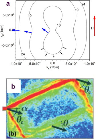
Figure 31. (a) Example of isofrequency curves and focusing for a 50 nm permalloy film with an applied field of 1 kOe. The numbers indicate the frequency in GHz. The blue arrows indicate directions of strong focusing. Small black arrows indicate regions with no focusing. (b) Experimental observation of focused beams in YIG from a small opening on left side. Reprinted (figure) with permission from [196], Copyright (2010) by the American Physical Society.
Download figure:
Standard image High-resolution imageAn experimental demonstration of focusing in a thin YIG film which is 7.7 microns thick is shown in figure 31(b). The source for the waves is a small channel on the left side. The energy flow is observed using microfocus BLS. It is immediately obvious that the energy leaving the channel does not display a diffractive type behavior as expected for an opening that is not small compared to the wavelength. Instead, one sees two narrow beams leaving the source, in agreement with what one expects from an analysis of the group velocities. It also interesting to note the reflection properties of these beams when they hit the edge of the sample. For waves in isotropic media, one expects the incident angle to be the reflected angle. Whereas the position where the wave hits the boundary acts like a new source as one expects, the beams produced propagate in one of the preferred directions, rather than producing a reflected wave front.
Spin systems have recently been investigated with the idea that spin waves could encode and process information with significant reductions in energy consumption when compared to electronic circuits. The fact that spin waves of different frequencies will be sent in different directions from a point source offers multiple practical advantages. For example, one can: (1) envision a magnonic de-multiplexer [197, 198] where multiple frequencies enter an antenna and are automatically sent in different directions according to their individual frequencies; (2) create narrow spin wave beams without the need for physical waveguides, and (3) tune the direction of a spin wave beam by changing the magnitude or direction of a static magnetic field or electric field [199], thereby allowing logic devices to be developed.
Up to this point, we have discussed the focusing of spin waves in ferromagnetic films with thicknesses ranging from 10 nm to a few microns. For these materials, internal dipolar fields provide the anisotropy required to cause focusing and caustics. However, for ultrathin ferromagnetic films only 1–2 nm in thickness, the anisotropy caused by dipolar effects is minimal and the constant frequency curves are nearly circular. Interestingly, there are several methods to produce and control caustic beams in this limit. One example occurs in thin ferromagnetic films which lie on top of a substrate that induces an iDMI. In this case, the combination of the dipolar effects with the DMI can not only produce caustic beams, but create nonreciprocal caustic beams [200] where beam in the x direction does not have an equivalent beam pointing in the −x direction.
An example of nonreciprocal caustics is shown in figure 32 for a 2 nm thick film in an external field of μ0
H0 = 0.8 T. The top panels show isofrequency curves for two different frequencies. The middle panels show the focusing pattern calculated analytically, and the bottom panels present micromagnetic simulations illustrating the spin wave energy as a function of position, calculated from the time average of an oscillating component of the magnetization,  , over two periods following 150 periods of oscillation. The results are dramatic. For example, at 4.2 GHz the isofrequency curve has a very flat region on the left side and a rounded region on the right side. This leads to a single beam propagating in the −x direction.
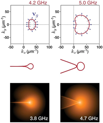
Figure 32. Isofrequency curves and the resulting focusing pattern for a thin ferromagnetic film influenced by iDMI. There is a magnetic field (vertically) parallel to the xy plane. The figures in the top panel show the isofrequency curves and the bottom sets of panels present the focusing patterns calculated analytically and numerically. Reprinted (figure) with permission from [200], Copyright (2016) by the American Physical Society.
Download figure:
Standard image High-resolution imageA second method to create and modify caustics in ultrathin films has recently been investigated [201]. All of the previous examples dealt with wavelengths that are large compared to a lattice constant. When one looks as high wavevector spin waves, the lattice structure itself can create anisotropic isofrequency curves, with the resulting focusing of energy flows.
17.2. Current and future challenges
Large scale applications for ferromagnetic spin waves in magnonic computing may require creation of multiple beams and methods to tune the focusing on a small, local scale. It will be necessary to investigate a number of options, including tuning the focusing by local magnetic fields and/or by polarized spin currents.
Recent advances in microscopy techniques may allow focusing effects to be probed on extremely short length scales. This might require artificial point sources such as anti-dots [202]. Progress in spin wave imaging with NV-center magnetometry allows caustics to be imaged with high spatial resolution [203], which opens up new avenues of exploration for short-wavelength spin waves in ultrathin films. Moreover, such detection techniques could be implemented with a spatial array of sensors, which could pave the way toward information processing with caustics.
Focused beams can also occur for systems with fast spin dynamics. For example, spin waves in antiferromagnets coupled to electromagnetic fields are polariton excitations with frequencies in the THz range. Dispersion relations for these waves can be highly anisotropic and display fascinating features such as the Goos–Hänchen effect and negative refraction. Formation of tunable caustics, a three-dimensional analogy to the focusing described here, is predicted for beams transmitted through thin antiferro- and ferri-magnetic films. Moreover, some multiferroics with magneto-electric coupling display exotic spin orderings and chiral interactions that lead to highly anisotropic electromagnetic energy flows at short wavelengths. These materials may offer new possibilities for electric and magnetic field control of focusing.
17.3. Concluding remarks
Because, in part, of the potential applications, the field of focused power flows outlined above is continuing to expand and appear in a variety of different areas. In addition, focused beams may allow us to learn about issues such as tunable heat transport or tunable transport of angular momentum. Given the range of applications and fundamental issues, the field of focused power flows in magnetic materials is likely to flourish.
Acknowledgments
RLS: acknowledges the support of the Natural Sciences and Engineering Research Council of Canada (NSERC). Cette recherche a été financée par le Conseil de recherches en sciences naturelles et en génie du Canada (CRSNG). REC thanks UCCS for Distinguished Professor research funding.
18. Voltage-controlled magnetic anisotropy induced spin waves
Bivas Rana1 and YoshiChika Otani1,2
1RIKEN, Japan
2University of Tokyo, Japan
18.1. Status
Apart from fundamental interests, the magnonics also aims to find out efficient ways to excite and manipulate spin waves (SWs) for the development of future magnonic devices, which will eventually surpass the operational speed, efficiency, functionality, integration density of current semiconductor-based electronic devices. So far, the SWs have been excited by conventional charge current, light, and thermally induced methods, such as radio-frequency current-induced Oersted fields, spin-transfer-torques, femtosecond pulsed laser beams, and thermal energy. Despite having some advantages, all these methods also have several disadvantages such as high energy dissipation in the form of Joule heating, instability of the miniaturized electrical junctions due to high current density, the difficulty of integration in nanoscale devices, excitation of coherent SWs, i.e., excitation of magnons in the ballistic regime and so on.
As an alternative, the excitation of SWs by electric-field is highly desirable. Importantly, the electronic spins localized in partially filled orbitals govern the magnetic properties of ordered magnetic materials. Although external electric-field cannot directly couple with those localized spins, it can interact indirectly with the spins via several means. In ferromagnetic semiconductors, electric-field modulation of carrier density controls the spins. In multiferroic materials, the strong coupling between magnetic and electric polarization enables us to control the spins by electric-field. In piezoelectric materials, the electric-field induced strain can deform an adjacent magnetostrictive ferromagnetic film (e.g., Ni), where the lattice deformation couples with the spins through SOC, known as magnetostriction. In the quest of a new electric-field induced method, the VCMA has emerged as a novel means to control the spins by electric-field. The PMA occurs at the interfaces between ultrathin 3d transition ferromagnetic (FM) metals (e.g., Fe, CoFeB) and nonmagnetic insulators (e.g., MgO, Al2O3) due to the hybridization of out-of-plane 3d orbitals of FMs and out-of-plane 2p orbitals of O (figure 33(a)). The electric field applied at the FM/oxide interfaces changes the electronic population significantly in the out-of-plane 3d orbitals of FMs compared with in-plane orbitals (figure 33(b)), eventually modifying the interfacial orbital hybridization and controls the interfacial spins through relativistic SOC of FMs [204].
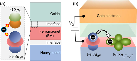
Figure 33. (a) Schematic diagram shows the origin of PMA at FM/oxide interface due to hybridization of out-of-plane 2p orbitals of O and out-of-plane 3d orbitals of FM. (b) The schematic illustration shows the mechanism of VCMA. When dc gate voltage VG is applied, the charge density at the out-of-plane 3d orbitals of FM is changed with respect to the in-plane orbitals. This affects interfacial orbital hybridization and changes PMA through SOC of FM.
Download figure:
Standard image High-resolution imageAs VCMA relies upon the modification of electronic population in 3d orbitals of FM, it is suitable for microwave applications. The excitation of FMR [205] and SWs [206, 207]in the gigahertz regime have been demonstrated with ultralow power consumption, which can be at least two orders of magnitude lower than the current induced spin-transfer-torques excitation. The coherent propagating SWs can be excited by placing a metal gate electrode on top of the oxide layer and applying RF voltage across the gate electrode and FM (figure 34(a)). The RF electric field at the FM/oxide interface modulates interfacial PMA and excites SWs at the resonance condition. The excited SW amplitude is linearly proportional to the RF voltage [206]. The maximum wavenumber of excited SWs is given by the inverse of the lateral width of the gate electrode. One of the key advantages is that the VCMA excitation is local, and the excitation area is right underneath the gate electrode. This enables to utilize VCMA in nanoscale devices with high integration density. Although VCMA cannot excite coherent SWs when the magnetization is aligned either in-plane or perpendicular to the film because of zero VCMA torque, these particular magnetization configurations are suitable for nonlinear parametric excitation of SWs. In this case, the time-varying VCMA couples to the out-of-plane component of dynamic magnetization with elliptical trajectory (figure 34(b)) [207]. Therefore, SW frequency is half of the frequency of VCMA (figure 34(c)) [208]. The critical advantage of parametric excitation is that it can efficiently excite and selectively amplify even shorter wavelength SWs. Unlike linear excitation, the parametric excitation requires a threshold power which depends upon excitation frequency, SW wavevector, the width of waveguide and gate electrode.
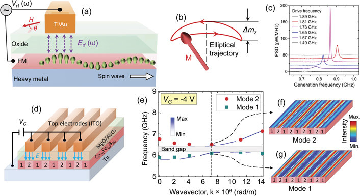
Figure 34. (a) Schematic illustration shows the excitation of coherent propagating SWs by VCMA. (b) Schematic diagram illustrates the magnetization precession in an elliptic trajectory. The out-of-plane component (mz ) of magnetization precession oscillates at a frequency twise than the in-plane components (mx , my ). (c) Power spectral density of the microwave signal emitted by a MTJ under VCMA induced parametric excitation. Curves are vertically offset for clarity and are listed in order of drive frequency. The figure is reproduced from reference [208]. (d) Periodic nature of electric field applied at CoFeB/MgO interface through periodically arranged metal gate electrodes, giving rise to two periodic regions: region 1 (outside of top electrodes) and region 2 (underneath the top electrodes). (e) Experimentally measured frequency versus wavevector dispersion at VG = −4 V under the application of 200 mT bias magnetic field. Symbols represent measured SW frequencies, while blue lines denote SW intensities as calculated by plane wave method. The corresponding color map is given inside. The dashed vertical line indicates the position of anticrossing, and the corresponding magnonic band gap is shown by the shaded region. (f) and (g) Calculated spatial profiles of the SW modes for wavevector k = 7.1 × 10⁶ rad m−1 under the application of VG = −4 V at μ0 H = 200 mT. Low frequency mode, i.e., mode 1 is confined in region 1 and high frequency mode, i.e., mode 2 is confined in region 2.
Download figure:
Standard image High-resolution imageApart from excitation, the modulation of SW properties (e.g. frequency) by VCMA have also been demonstrated [209]. The VCMA can also be utilized for the formation of reconfigurable nanochannels for SW propagation [210]. When a number of parallel nanochannels are formed on an ultrathin ferromagnetic film by placing parallel gate electrodes and applying gate voltage, the parallel nanochannels can be used as 1D MCs (figure 34(d)). In absence of nanochannels, i.e., gate voltage, only a single SW mode with trivial dispersion is observed. Choudhury et al have experimentally demonstrated the presence of two SW modes with nontrivial dispersion curves separated by a tunable band gap in VCMA induced parallel nanochannels (figure 34(e)) [211]. The higher (mode 2) and lower (mode 1) frequency modes are confined within channel 2 and channel 1, respectively (figures 34(f) and (g)).
18.2. Current and future challenges
We have to sort out many challenges to fully utilize the advantages of VCMA in magnonic devices [212]. Although many experimental reports demonstrate the excitation and characterization of VCMA induced FMR [205, 213], only a couple of experimental reports, on the other hand, show the VCMA induced propagating SWs [206, 208], manipulation of SW properties by VCMA [209, 211] and control of damping constant by electric field [214]. Therefore, more experimental studies are necessary for understanding the properties and characters of VCMA excited linear and nonlinear SWs.
So far, it is observed that most of the applied microwave power is reflected back from the devices while exciting FMR, SWs by VCMA because of impedance mismatch [205]. In principle, impedance mismatch can be minimized by reducing the thickness of the oxide layer. However, it may significantly increase the junction current leading to many spurious effects such as spin-transfer-torque induced SWs, Joule heating, etc. Hence, the optimization of junction impedance to minimize electrical losses and impedance mismatch with an optimum value of the VCMA coefficient is a real technical challenge.
The VCMA coefficient for FM/oxide heterostructures can be up to 100 fJ V−1 m−1. One of the major challenges is to enhance the VCMA coefficient at least up to pJ V−1 m−1 to fulfill the minimum criteria for the potential application of VCMA in practical devices. This can be achieved by engineering FM/oxide interface. It has been observed that doping of HMs or insertion of an ultrathin heavy metallic layer such as Ta, Pt, W, Ir at FM/oxide interface can significantly enhance the value of the VCMA coefficient. The enhancement of the VCMA coefficient is also possible even by inserting the ultrathin layer of relatively lighter materials such as Hf, Mg. The physical reason behind this is the modification of orbital hybridization at FM/oxide interface and suppression of surface oxidization of the FM layer. However, the VCMA coefficient cannot be increased more than few hundreds of fJ V−1 m−1 by these methods. Alternatively, the VCMA coefficient can be further increased up to few pJ V−1 m−1 by utilizing voltage-controlled redox reactions, charge trapping, electromigration. As these methods rely upon the slow movement of ions, require thermal activation process and have very slow response time, they cannot be applied in microwave devices. However, they can be used for other purposes such as modulation of SW properties, formation of nanochannels and so on.
As VCMA is an interfacial effect, it is limited to ultrathin FM films. Growing high-quality thin films with a smooth and defect-free clean interface is therefore highly desirable. Although molecular beam epitaxy can grow high-quality ultrathin films, it is inapplicable for large scale production, i.e., for commercial purposes. Consequently, it is a real challenge to produce high quality thin films by dc or RF sputtering.
The overall damping constant of ultrathin FM films is generally higher than thicker films, which limits the SW propagation length down to micrometer distance. The SW amplifiers are essential to increase the propagation length by compensating the energy losses of SWs during propagation. Conventionally, charge current based spin–orbit-torque and parametric pumping methods are used to amplify SWs effectively. Alternatively, VCMA torque could also replace the charge current-induced torque to build up an energy-efficient amplifier. However, experimental demonstrations are lacking. Therefore, in addition to increasing the VCMA coefficient, the searching for FM materials with ultralow damping parameter is also getting equal importance. One may think about ferrimagnetic insulators and Heusler alloys as the possible alternatives; unfortunately, VCMA phenomena have not been observed yet in these materials.
Another future challenge will be the efficient detection of VCMA induced SWs or magnons in ultrathin FM films by electrical means. Recently, the local, quantitative, and phase-sensitive detection of the SWs have also been demonstrated by single NV centers in diamond. But, this method can increase the complexity of device fabrication as FM films need to be deposited directly on a diamond containing NV centers. Alternatively, MTJs can be used as an efficient way to detect SWs in ultrathin films. However, experimental demonstrations are still lacking.
Ultimately, the interaction of VCMA induced SWs with various types of spin configurations such as magnetic skyrmions, and domain walls need to be studied experimentally for the development of magnonic devices. For instance, the driving skyrmions, domain walls by VCMA induced SWs can be considered. Moreover, properties of the induced SWs in VCMA controlled reconfigurable nanochannels, 2D MCs, and magnonic logic gates need to be studied experimentally. Recently, interfacial PMA has also been examined in ultrathin FM films hybridized with 2D materials, showing a significant increment of interfacial PMA in these hybrid structures. Therefore, the study of VCMA phenomena and VCMA induced SWs may also pave the way for developing various types of voltage-controlled 2D magnonic devices. Consequently new ideas such as inducing in-plane magnetic anisotropy at FM/oxide interface by controlled magnetic annealing and electric field control of induced anisotropy [215] and inverse VCMA effect for detecting SWs are also getting importance due to possible technological advantages.
18.3. Concluding remarks
VCMA has emerged as a potential technique to excite and manipulate SWs in ultrathin FM films for the development of all-electric-field controlled low power magnonic devices. However, the VCMA operated magnonic devices are still in its infant stage of development. Indeed, we have to experimentally demonstrate all the theoretical proposals, such as VCMA induced parametric amplification of SWs, dynamic interaction of SWs propagating through voltage-controlled nanochannels [210], voltage-controlled logic gates, 2D MCs [216], SW caustics. Above all, it is indispensable to improve the VCMA coefficient by the interface and material engineering.
Acknowledgments
This review is supported by Grant-in-Aid for Scientific Research on Innovative Area, 'Nano Spin Conversion Science' (Grant Number 26103002). BR acknowledges RIKEN Incentive Research Project Grant No. FY2019, for partial financial support.
19. Indirect interactions between magnets
Weichao Yu1, Tao Yu2 and Gerrit E W Bauer,1,3
1Tohoku University, Japan
2Max Planck Institute for the Structure and Dynamics of Matter, Germany
3Groningen University, The Netherlands
19.1. Status
The exchange interactions between electron spins in condensed matter generates a rich variety of magnetic order. It becomes exponentially small at larger than atomic distances, so different magnets interact by exchange only when in direct contact. The weaker dipole interaction generates forces between macroscopic magnets that decay algebraically with distance. Magnets can also interact indirectly through a non-magnetic medium. Mobile electrons in metals mediate an oscillatory RKKY non-local exchange interaction over nanometers. The coupling by non-equilibrium spin currents through metal spacers can reach over micrometers. The exchange of spin waves synchronizes magnetic oscillators. Microwave photons in high-quality cavities are supremely suited to communicate spin information because of their coherence over large distances and the strong interaction of spin ensembles such as ferromagnets with the ac magnetic fields [217, 218]. Other waveforms such as magnons and phonons also generate indirect interactions between small magnets over relative large distances [76, 219]. In this roadmap article, we outline the interest of letting two or more ferromagnets interact in cavities or wave-guides for different mediating waveforms but with emphasis on microwaves.
In free space, magnets interact by the magneto-dipolar interaction, which is very weak for typical sub-nm magnetic spheres at cm distances. However, they may couple strongly over large distances by exchanging virtual photons in cavity modes. Interpreting the collective Kittel mode of a single magnet as a magnonic hydrogen atom, an interacting pair forms a magnonic hydrogen molecule with hybridized orbitals of even and odd symmetry (figure 35) [220]. When probed by an even cavity mode, microwave spectroscopy detects the first 'bright' mode, but not the second 'dark' one [217]. The (sub-radiant) magnons in the dark mode do not suffer from radiative damping and have longer decay time, which might be useful for quantum information storage [221]. The indirect interaction between magnets provides a large playground since the cavity as well as position, size and type of the magnets is arbitrary. Adding non-magnetic, but optically active structures and materials, is another important option. The task to systemize various configurations, to find new hybridizing mechanisms, and search for applications is a challenge that has only just begun.
19.2. Current and future challenges
Customizing cavities: cavities come in different shapes and types. Here we focus on microwave cavities formed by a closed box of high-quality metal that confines photons without significant losses. Small orifices do not disturb the system significantly and act as non-invasive input and output terminals that allow measuring the properties of the hybrid system in terms of the microwave transmission and reflection coefficients. When magnetization damping is small as well, the cavity + load system approximately conserves energy and the system Hamiltonian is (almost) Hermitian. The magnon–photon coupling is then coherent, and photon and magnon levels repel each other when tuned to degeneracy. CPWs are open cavities that offer greater flexibility, but are leaky, i.e. have a smaller quality factor. Waveguides are intrinsically open cavities that channel the free flow of microwaves with associated radiative damping. Dissipation may change the qualitative physics since a non-Hermitian Hamiltonian governs the non-local interaction between magnets [221].
The indirect coupling already modifies the ground state. When not at the minimum of the free energy, mechanical and magnetic torques and forces arise that can be modulated by the magnetic configuration and the frequency detuning. Heat current flow in the presence of temperature differences in the cavity. Feeding the cavity with microwaves from external sources, either via the input and output ports or local coils that address individual magnets [217], can drive the system into highly excited states [222].
Cavities or resonators can also confine optical photons, but the domination electric field coupling is relatively weak. An interesting challenge is the use of cavities in the intermediate THz radiation regime. Thin films confine phonons normal to thin films where they may form phononic spin valves [219], while magnon cavities can be induced by nanostructures on magnetic thin films [76].
Loading cavities: we may fill the cavities by magnets in different numbers and structural as well as magnetic configurations. Figure 36 shows as an example of a collinear magnonic benzene molecule driven by a microwave feed from the input port. We are not limited to ferro- or ferrimagnets, but may use antiferro- and paramagnets. The magnonic atoms may 'react' with other particles made from, e.g., ferroelectrics, superconductors, Josephson qubits [239], metamaterials, or devices such as MTJs.

Figure 35. The collective dynamics of a ferromagnetic particle (Kittel magnon) can be interpreted as ground state of a bosonic atom. The interaction between different atoms, enhanced by the exchange of photons in open or closed cavities, leads to collective delocalized states.
Download figure:
Standard image High-resolution image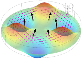
Figure 36. Numerical simulation of six magnetic spheres on a circle inside a disk-shaped microwave cavity fed by attached ports. At resonance, the magnetizations (black arrows) precess coherently in the presence of a unidirectional photon current as illustrated by the Poynting vector field (magenta arrows). The colored background is the electric field component in the perpendicular direction. We interpret this system as a chiral magnonic benzene molecule (Yu et al 2020, Phys. Rev. B 102, 064416).
Download figure:
Standard image High-resolution imageChiral interaction: in the absence of relativistic effects, the angular and linear momentum of photons, phonons, and magnons waves are in general independent. However, chirality emerges in DE surface spin waves or by spin waves excited by magnetodipolar stray fields [76]. Cavities or waveguides induce admixtures of TM and TE modes that generate local chirality at special lines. When the mediating waves are chiral, the indirect coupling between magnets is unidirectional. A consequence is the accumulation of magnons at the edge of a chain of magnets in a cavity [222]. It is then possible to design chiral magnonic molecules analogous to conventional aromatic molecules, but with non-reciprocal magnon couplings and persistent currents (figure 36), facilitating the design of novel on-chip microwave isolators and circulators. Since spin waves in thin film can be chirally excited by magnetic stray fields, similar games become possible on a much smaller scale. The acoustic Rayleigh surface waves display rotation–momentum coupling and generate novel indirect couplings [223].
Toroidal moment: the toroidal dipole moment or anapole is a parameter to describe the electromagnetic far field, which is independent from the magnetic and electric dipoles [224]. Spatially distributed magnets can contribute either static or dynamic toroidal multipoles, which have peculiar response and radiating properties. As discussed above, in a microwave cavity loaded by magnets, chiral spin currents may flow by means of cavity photon exchange. We anticipate that an exchange-strained circular spin texture generates equilibrium spin currents and associated toroidal moments, while injected microwaves in the configuration of figure 36 generates a giant dynamic anapole.
Toward quantum: strongly coupled microwave photons can drive a weakly damped magnonic system easily into the non-linear regime, which is an important prerequisite for interesting quantum effects such as quantum entanglement and quantum squeezing. Non-linearities generate highly entangled magnon–photon states or generate tripartite entanglement between magnons, photons and phonons [225].
19.3. Concluding remarks
Magnons in spatially separated magnets may hybridize by the coherent exchange of (quasi)particles such as photons, phonons, and continuum magnons. Coupled magnet assemblies form very flexible devices on various length scales. AC and DC magnetic fields easily manipulate their collective bosonic excitations, offering a unique platform to study quantum effects and test new functionalities needed for next-generation information technologies.
Acknowledgments
This work was supported by JSPS Kakenhi (Grant No. 19H00645 and No. 20K14369). TY acknowledges financial support by Deutsche Forschungsgemeinschaft through the Emmy Noether Program (SE 2558/2-1).
20. Topological magnonics
Christian Back1 and Götz S Uhrig2
1Technical University of Munich, Germany
2Technical University of Dortmund, Germany
20.1. Status
Generally, topological effects in condensed matter display a certain robustness against perturbations such as imperfections and disorder resulting from sample growth and patterning. This idea extends also to magnonics and motivates to consider and to realize topological effects. A second appealing feature of topological magnetic excitations is their generic chirality. Their edge modes travel only in one particular sense, see figure 37, and section 16. Recently, it has been proposed that magnonic topological edge modes in ferromagnetic domains can be used for advanced information processing [226]. This route is promising because it can be hoped that such systems are less dissipative. If the magnons can be manipulated coherently quantum information processing comes within reach. This perspective has triggered a surge of interest in topological magnonics in recent years which makes it impossible to review them here so that we refer to a longer survey for a more complete list of references [227].

Figure 37. Schematic illustration of a propagating chiral magnon localised at the edge of a confined sample realizing a ferromagnetic Shastry–Sutherland lattice, for details see reference [233].
Download figure:
Standard image High-resolution imageNotwithstanding the obvious interest in topologically protected magnon modes, the experimental reports concerning topological magnonics are still scarce and can be grouped into two categories: detection of the magnon Hall effect, e.g. [228–230], and observation of topological magnon bands e.g. [231, 232].
In 2010, Onose et al [228] reported a transverse magnon current in the insulating collinear ferromagnet (FM) Lu2V2O7 with pyrochlore structure. In this system and in similar pyrochlore compounds (Ho2V2O7, In2Mn2O7, Lu2V2O7, and the quantum spin ice system Tb2Ti2O7) [229] as well as in the material YIG [230], a transverse magnon current has been observed. Notably, the detection of the magnon Hall effect has been realized in insulating materials only so far, where a temperature gradient drives the magnon current. Detection is realized by thermal Hall effect measurements [228, 229] or, in the case of YIG, by direct observation of a temperature difference [230]. In the classical pyrochlore materials [228] the rather strong DMI is at the origin of the generation of a Berry curvature of the magnon bands which leads to the transverse deflection of the exchange dominated magnon current, see also section 13. In YIG [230], DMI is weak and the explanation of the origin of the sideways deflection of long-wavelength magnons in the dipole-exchange regime should be revisited.
In the large class of antiferromagnets, in many materials with strong SOC the DMI is strong enough to have a significant impact on the magnon band structure and non-collinear order may be induced [232]. In particular, quasi 2D kagome or honeycomb materials are of interest, where flat, topological magnon bands have been predicted and recently detected using thermal Hall and inelastic neutron scattering experiments [231, 232].
20.2. Current and future challenges
So far, topological effects have been measured in a limited number of systems which are mostly magnetically ordered so that the excitations are magnons of which the total number is generically conserved except if certain anisotropies are present, e.g., dipolar interactions [233]. Thermal Hall measurements have confirmed non-trivial topology. Clearly, the measurements of further properties providing evidence for topological behavior are called for. In parallel, it is of great current interest to identify more magnetic systems with non-trivial topology, for a class of potential candidates, see reference [234] and figure 38. In addition, completely novel ideas such as using Moiré bands of twisted ferromagnetic bilayers are proposed [235]. It would be highly advantageous to find systems with larger exchange coupling and concomitantly larger couplings such as DMIs inducing the required Berry curvatures. The advantage of larger couplings is twofold: the phenomena can be detected at higher temperatures and they occur on shorter time scales. The latter point is essential if one wants to move from equilibrium properties to non-equilibrium physics which is obviously needed to tackle switching and information processing.
Figure 38. Panel (a) Shastry–Sutherland lattice formed in a rare earth (RE) silicide (two-dimensional projection). Panel (b) magnonic dispersion in a strip of the lattice in (a) extended in a-direction, confined in b-direction, for spin S, exchange coupling J, single-ion anisotropy A = 0.2J, and DMI Dz = 0.25J in z-direction. The dispersion of the right-moving chiral edge mode is shown in orange, the one of the left-moving in blue, for details see reference [234].
Download figure:
Standard image High-resolution imageIn addition, the extensions of the current scope on ferromagnetic magnons to antiferromagnetic (AFM) magnons as such [236] or on top of non-collinear spin textures [237] as well as to other magnetic excitations represent fascinating challenges, both in concepts and for applications. Fundamentally, AFM magnons are different from FM magnons in that they display linear dispersions and that their number is not conserved. The linear dispersion leads to larger frequencies and faster dynamics at given length scales. Note, however, that experimental detection of magnon modes in AFMs is much more challenging and suitable experimental methods are to be developed. Beyond magnons, there are further intriguing excitations for instance fractional spinons which may be relevant in quantum spin liquids [229] and triplons in valence bond solids [238]. For the latter, non-trivial topology is verified by inelastic neutron scattering and they are protected by an energy gap.
Looking further ahead, the control and manipulation of topological magnetic excitations must be targeted, requiring to enter the field of non-equilibrium physics. Certainly, this represents a formidable challenge. Is it possible to create, to manipulate and to detect wave packets of magnons or even single excitation? Can this be achieved coherently? Which techniques are promising? A possible candidate is optical control by laser pulses, e.g., exploiting the inverse Faraday effect [239].
Finally, one may ask if realizable device concepts utilizing topological magnonics can be developed. This would require first of all theoretical concepts, but also clear recipes toward experimental realization. Ideally this would encompass room temperature operation and a selection of materials that are easily fabricated by standard deposition tools.
One could expect, for example, that transverse magnon currents are observable e.g. in a micro-focus BLS, experiment by observing magnon deflection in a temperature gradient. Given the superior sensitivity of BLS such an experiment on bulk samples might be feasible. Furthermore, one can foresee the design of magnetically ordered nanostructures where chiral edge current may be detectable using bespoke spin-to-charge conversion designs.
20.3. Concluding remarks
In summary, the field of topological magnonics is still at its infancy, but it holds great promise. Experimentally it is obviously difficult to realize materials that clearly show topological magnon bands or that show clear manifestations of effects that are based on topology such as the magnon Hall effect. On the theory side, concepts for novel effects need to be developed which put the particular properties of topologically protected modes to use. The possibility to tailor the spin wave velocity of magnonic edge modes is an example for such a concept.
Acknowledgments
CB acknowledges fruitful discussion with Takuya Taniguchi; GSU thanks Maik Malki for useful discussions and providing the figures.
21. Low- and room-temperature hybrid magnonic heterostructures
Oleksandr V Dobrovolskiy1, Barbora Budinska1, Huajun Qin2 and Sebastiaan van Dijken2
1University of Vienna, Austria
2Aalto University, Finland
21.1. Status
Hybrid magnonic systems have recently attracted great attention because of emerging fundamental physical phenomena unseen in their elementary building blocks and due to their application potential, particularly, in coherent information processing [240]. They provide a modern paradigm for combining platforms and devices based on strong coupling between excitations in the charge, lattice and spin degrees of freedom and allow for tailoring the response of the system in one degree of freedom via tuning the excitations in the other one [241]. Magnons are highly tuneable excitations and can be engineered to couple with various dynamic media and excitations such as photons [240], phonons [241], fluxons [242] etc. This section deals with only two types of hybrid magnonic systems—ferromagnet/superconductor and ferromagnetic/ferroelectric heterostructures. Recent reviews devoted to hybrid magnonic systems of various other types can be found, e.g. in references [240, 241, 243].
21.2. Ferromagnet/superconductor hybrid structures for cryogenic magnonics
Traditionally, magnonics is a room-temperature research domain. However, recent studies are extending magnonics to cryogenic temperatures [221, 242, 244, 245]. This extension is driven by investigations of strongly coupled light-spin hybrid systems for quantum computing that approach the quantum limit of excitation [221]. In addition, thermal effects such as reduced saturation magnetization and thermally activated motion of topological defects are less pronounced at low temperatures, that leads to new phenomena in the spin-wave dynamics. Importantly, in cryogenic magnonics, microwave experiments are often performed in environments of superconducting quantum circuits and various hybrid devices based on Josephson junctions. Because of experimental constraints for light intensities in a purely optomagnonic system, quantum magnonics requires hybridized systems of magnon excitations and nonlinear macroscopic quantum systems such as superconducting qubits [221], see figure 39(a). At the same time, ferromagnetism (F) and superconductivity (S) entail opposite spin orders and thus their combination gives rise to numerous novel phenomena [242, 244, 245]. However, so far coexistence of F and S in bulk systems remains a rare circumstance peculiar to complex compounds in which either a strong ferromagnetic order coexists with unconventional spin-triplet superconductivity or orbital coupling stipulates coexistence of antiferromagnetic order (section 15) with conventional spin-singlet superconductivity.

Figure 39. Examples of ferromagnet/superconductor hybrid structures for cryogenic magnonics. (a) Strong dispersive regime of quantum magnonics. Interaction of strength gq-m between the Kittel mode (with frequency ωm) of a spherical ferrimagnetic crystal of YIG and a superconducting qubit (ωq), engineered through magnetic- and electric-dipole couplings to a microwave cavity mode (top). Normalized qubit spectrum measured as a function of the coil current (bottom) and at ωq ≈ ωm (right). From [221]. Reprinted with permission from AAAS. (b) Magnonic metamaterial on the basis of S/F hybridization: patterned Py films are placed onto a CPW made of Nb. Black and green arrows show the direction of the microwave propagation and of the external magnetic field. [245] John Wiley & Sons. [Copyright © 2018 WILEY‐VCH Verlag GmbH & Co. KGaA, Weinheim]. (c) Bragg scattering of spin waves on the Abrikosov vortex lattice in a Py/Nb bilayer. Spin waves are excited by antenna 1, propagate through the Py waveguide and are detected by antenna 2. The vortex lattice induces a spatially periodic magnetic field h(x, y) in Py, which becomes alternating in time when the vortices move under the action of a transport current. Bragg scattering of spin waves on the moving vortex lattice is accompanied by the Doppler effect. The tunability of the vortex lattice parameter via changing the out-of-plane component of the magnetic field H⊥ allows for engineering of the spin-wave transmission spectrum. Reprinted by permission from Springer Nature Customer Service Centre GmbH: [Springer Nature] [Nature Physics] [242] (2019). (d) Cherenkov excitation of magnons by fast-moving fluxons. Vortex lattice moving with the velocity v induces a spatially periodic ac magnetic field h(x, t) which excites the system of magnetic moments shown by purple arrows (top). This additional dissipation results in current peaks in the I–V characteristics (bottom). An additional magnetic (M) viscous force adds up to the BS viscosity due to vortex core alone, resulting in a voltage drop for currents above Ion corresponding to some threshold vortex velocity vc. Reprinted (figure) with permission from [246], Copyright (2011) by the American Physical Society.
Download figure:
Standard image High-resolution imageThe coexistence of S and F can be readily achieved in artificial S/F heterostructures which allow for numerous approaches for S/F hybridization. For instance, in proximity-coupled (i.e. electrically contacted) S/F/S three-layers in in-plane fields, a substantial reduction of the FMR field [244] is attributed to the generation of unconventional spin-triplet superconductivity and to an interplay of the F layer with S-induced magnetic flux. In particular, it has been established that the presence of a spatially varying magnetization at an S/F interface can generate spin-polarized triplet supercurrents via spin mixing and spin rotation processes. In case of proximity-decoupled S/F bi-layers in in-plane fields, see figure 39(b), it has been demonstrated experimentally that coupling of spin waves in F with S results in an enhanced phase velocity of the spin waves [245]. This enhancement occurs due to the Meissner screening of ac magnetostatic stray fields by S and it opens access to the development of a new class of metamaterials on the basis of S/F hybridization [245].
A number of novel effects have been observed experimentally for proximity-decoupled S/F bi-layer systems in out-of-plane magnetic fields [242]. When the S layer is in the mixed state, an external magnetic field penetrates it in the form of a lattice of Abrikosov vortices (fluxons). In proximity-decoupled S/F bi-layers, the stray fields emanating from the vortex cores produce a periodic modulation of the magnetic order in F, such that the S/F bi-layer can be viewed as a fluxon-induced MC (section 2). In such a MC, see figure 39(c), forbidden-frequency gaps (bandgaps) are formed for spin waves with Brillouin wavenumbers that correspond to the period of the vortex lattice [242]. The tunability of the vortex lattice parameter via changing the out-of-plane component of the magnetic field allows for engineering of the spin-wave transmission spectrum. Remarkably, experiments on Bragg scattering of spin waves on a flux lattice moving under the action of a transport current in the S layer have revealed that it is accompanied by Doppler shifts [242]. One further promising research direction is related to the experimental examination of the radiation of magnons by moving fluxons via a Cherenkov-type mechanism. The Cherenkov radiation of magnons by fluxons is expected when the vortex velocity exceeds some threshold value and, as predicted theoretically [246], it should to lead to peaks in the current–voltage curve and an additional magnetic (M) contribution to the Bardeen–Stephen (BS) core viscosity, see figure 39(d). Given the vortex lattice parameter which in the presence of out-of-plane fields between 2 T and 10 mT varies from 35 nm to 500 nm, Cherenkov radiation of short-wavelength magnons (section 7) by fast-moving vortices could become a route to the excitation of exchange-dominated spin waves in S/F heterostructures and antiferromagnetic superconductors.
21.3. Ferromagnetic/ferroelectric heterostructures for programmable magnonics at room temperature
Studies of coupled magnetic and ferroelectric (FE) phases are motivated by fundamental questions about ferroic order coexistence and their potential for low-power nanoelectronic devices. Hybrid ferromagnetic (FM)/FE materials in which magnetoelectric interactions arise from charge modulation, exchange coupling, or strain transfer at composite interfaces are particularly promising because they allow for electric-field control of magnetism at room temperature [247]. In addition, FE domains can be imprinted into a FM film to form a programmable metamaterial without physical patterning [248, 249]. Here, we review magnonic phenomena arising from strong local coupling of FM and FE order parameters. Sections 8 and 18 describe electric-field manipulation of spin waves using piezoelectrics and gate dielectrics.
Recent studies exploiting FM films grown onto FE BaTiO3 substrates have highlighted the potential of such hybrids for active spin-wave control. In this material system, local strain transfer from 90° stripe domains in BaTiO3 induces a regular modulation of magnetic anisotropy in the adjacent FM film via inverse magnetostriction. If the magnetoelastic anisotropy dominates other magnetic energies, the two ferroic domain patterns correlate (figures 40(a) and (b)). Because domain walls in FE materials are only a few nanometres wide, the induced changes of anisotropy in the FM film are nearly abrupt. This has two important consequences; sharp lateral variations of the effective magnetic field and strong pinning of magnetic domain walls onto their FE counterpart.
Figure 40. (a) Schematic of a FM/FE heterostructure exhibiting full domain-pattern transfer. The spontaneous polarization and lattice tetragonality of the FE layer rotate by 90° at the FE domain walls. Through strain transfer and inverse magnetostriction, this induces an alternating uniaxial magnetoelastic anisotropy in the FM layer. The magnetization aligns along the anisotropy axes in zero magnetic field (arrows). (b) Polarization and Kerr microscopy images of the FE and FM domain structures in a 50 nm CoFeB/BaTiO3 bilayer. (c) Formation of fifth order standing spin waves in every second stripe domain of the same heterostructure during uniform excitation (simulation) [250]. (d) Emission of propagating spin waves from an anisotropy boundary in the FM/FE heterostructure and the simulated spin-wave dispersion curves for a 60 mT bias field along and perpendicular to the uniaxial magnetic anisotropy of the stripe domains [250]. (e) Kerr microscopy images demonstrating switching between magnetic stripe domains with alternating head-to-head/tail-to-tail domain walls (top) and head-to-tail domain walls (bottom). The blue scale bar corresponds to 10 μm. (f) Schematic of a micro-focused BLS experiment for the analysis of spin-wave transmission through a programmable pinned magnetic domain wall. The orange scale bar corresponds to 2 μm. (g) Demonstration of strong spin-wave reflection if the pinned domain wall is set to a narrow head-to-tail state and nearly full spin-wave transmission after its structure is switched to a broad head-to-head configuration [132]. The BLS scans are performed near the frequency of an antinode resonance mode in the narrow domain wall.
Download figure:
Standard image High-resolution imageThe modulation of magnetic anisotropy in strain-coupled FM/FE bilayers confines the excitation of spin-wave modes to single stripe domains, as demonstrated experimentally in reference [250]. At low frequency, standing spin waves form only in domains with small effective field (every second stripe), allowing spin-wave localization and guiding (figure 40(c)). Additionally, the narrow anisotropy boundaries act as local sources of propagating spin waves under uniform microwave excitation (figure 40(d)). Micromagnetic simulations indicate that the wavelength of the emitted spin waves scales down well into the exchange-dominated regime, enabling short-wavelength magnonics (section 7). Mode localization and short-wavelength spin-wave emission persist up to large magnetic field, facilitating active tuning of the spin-wave frequency and wavelength [250].
Strong pinning of straight magnetic domain walls in FM/FE heterostructures offers various other magnonic prospects. For instance, when driven into periodic oscillations by a spin-polarized ac electric current, the domain walls act as a local source of propagating spin waves [251]. Additionally, spin-wave transport through pinned magnetic domain walls can be actively turned on and off by reversible switching between two non-volatile domain-wall spin textures [132]. This programmable effect, illustrated in figures 40(e)–(g), is explained by a large difference in domain-wall width if the magnetization is set to a head-to-head/tail-to-tail or a head-to-tail configuration.
Electric-field control of spin waves in FM/FE bilayers with correlated domain patterns is a logical next step. Switching of the spontaneous polarization reorients the unit cell of the FE material (figures 40(a) and (b)) and, via strain transfer, this alters the direction or strength of the magnetoelastic anisotropy in the FM film. Local magnetic switching, the writing and erasure of magnetic domain patterns and reversible motion of magnetic domain walls in an electric field are demonstrated already [249]. For magnonics, the ability to move magnetic domain walls and switch the anisotropy by low-power electric fields offers an attractive new approach for active spin-wave manipulation. Reports along this research direction will likely appear in the coming years.
21.4. Current and future challenges
Given that magnetic moment couples to the current oscillations in hybrid Josephson junctions, care should be taken in the analysis of their FMR response and current–voltage characteristics [244]. Bloch-like band structures in the spin-wave transmission spectra of S/F bilayers require long-range order of the vortex lattice [242] which is hard to achieve in experiments. For the Cherenkov-like generation of magnons by moving fluxons, vortex velocities exceeding 1–3 km s−1 are required [246]. At such high velocities vortex cores may collapse because of the flux-flow instability. To prevent instability, one can use, e.g., vortex guiding in S/F bilayers or superconductors with fast relaxation of disequilibrium, for which vortex velocities of 5–15 km s−1 have recently been demonstrated [252].
Electric-field control of magnetism in FM/FE heterostructures offers a low-power mechanism for spin-wave manipulation at room temperature. To date, proof-of-principle experiments utilize thick single-crystal FE substrates, necessitating the use of relatively large voltages [249]. For practical devices, the voltage pulses should be substantially smaller. Epitaxial FE films could satisfy this requirement [248]. Yet, the growth of thin films with regular FE stripe domains is challenging. Many attractive magnonic features of FM/FE bilayers originate from a regular modulation of magnetic anisotropy and strong pinning of straight magnetic domain walls. Similar effects could be realized also in other material systems, for instance via local ion-beam irradiation of FM films.
21.5. Concluding remarks
Investigations of S/F hybrid structures are gaining a momentum, opening access to exciting emerging phenomena in spin-wave physics and advancing novel magnonics and spintronics functionalities. The extension of magnonics to cryogenic temperatures has given birth to the new research direction of magnon fluxonics and metamaterials on the basis of F/S hybridization. Moreover, S/F heterostructures allow for highly efficient magnon–photon coupling and, thus, are of crucial importance for the further development of quantum magnonics.
Heterostructures with coupled FM and FE order parameters have emerged as an attractive material platform for room-temperature programmable magnonics. Imprinting of FE domains into a FM film has enabled new approaches for short-wavelength spin-wave emission, magnonic guiding, and spin-wave manipulation through magnetic- and electric-field actuation. Integration of these magnonic effects in magnetoelectric devices promises new functionalities and low-power operation.
Acknowledgments
OVD acknowledges financial support by the European Cooperation in Science and Technology via COST Action CA16218 (NANOCOHYBRI) and ERC Starting Grant 678309 MagnonCircuits. HQ acknowledges financial support from the Academy of Finland (Grant Nos. 317918 and 325480). SvD acknowledges financial support by the European Research Council (Grant Nos. ERC-2012-StG 307502-E-CONTROL, ERC-2014-PoC 665215-EMOTION and ERC-PoC-2018 812841-POWERSPIN) and the Academy of Finland (Grant No. 321983).
22. Biologically encoded magnonics
Benjamin W Zingsem1 and Michael Winklhofer2
1The University of Duisburg-Essen, Germany
2The Carl von Ossietzky University of Oldenburg, Germany
22.1. Status
Biologically encoded magnonics or biomagnonics, for short, is a recent approach to magnonics research, wherein biogenic magnetic material is harnessed for magnonics applications. Magnetotactic bacteria present an ideal model system for biomagnonics studies. These microorganisms have the genetic machinery to form dedicated ensembles of magnetic nanoparticles—magnetosomes—for orientation by the Earth's magnetic field. The magnetosomes consist of a strongly magnetic material (magnetite, Fe3O4), have magnetic-single domain character, and are arranged in the form of one or several linear chains [253]. Each magnetic particle is enclosed in a membrane vesicle, which not only controls the shape and size of the particle (<100 nm) but also keeps adjacent particles separated by a clear distance of 8–10 nm [253]. Thereby, the particles are not exchange-coupled among each other but interact solely by their stray fields. The spatial distribution of the stray fields, and thus the spin-wave spectrum, depends on the geometric arrangement of the particles, which, in turn, is biologically controlled. The mode profile, i.e., the spatial distribution of phase and amplitude, of spin-waves in magnetic nanoparticles exhibits distinct differences from larger systems: at gigahertz excitation frequencies (⩽20 GHz at ca 300–400 mT), each nanoparticle responds with a uniform precession [254]. Dipolar pinning, which is known to unfavourably distort the mode profiles near the edges of a large continuous sample [255], is suppressed in nanoparticles due to the strong, short-range exchange coupling. This entails a macrospin behavior where each individual nanoparticle acts as a coherent oscillator. At the same time, wavelengths that are shorter than typical low-frequency exchange- or dipolar spin-waves, can be accommodated in particle chains by forcing neighboring particles to oscillate with different phases. It was also observed in [254, 255] that nanoconfinement leads to coherent oscillation and a significant reduction in spectral linewidth, i.e., reduced damping, even compared to homogeneous bulk samples.
An instructive example of a suitable magnonics device based on dipolar interactions are three single-domain particles arranged around the corner. The spectral response of such a system to a spatially uniform excitation reveals an intriguing magnonic property at an applied field angle of 45° (figure 41(a))–a spectral gap. The origin of the gap can be rationalized from the analysis of spatial mode profiles in the system. The relevant modes are the high energy mode (figure 41(b-i)), where the particles precess all with the same phase, and the low energy mode (figure 41(b-ii), where the corner-particle is locked to an anti-phase oscillation with respect to the end particles. Having incommensurate spatial mode profiles (figure 41(b)), these two normal modes (eigenstates) repel each other when approaching 45°, hence the spectral gap. Importantly, an eigenstate can also be excited by driving just a single particle at the eigenfrequency of the corresponding eigenstate; the energy from the local driving force is transmitted into collective oscillations through dipolar coupling among the particles. By driving a second particle at the same frequency, the eigenmode can be sustained or annihilated, depending on the phase difference between the two driving forces. For example, in the high-energy eigenmode, the spin-wave amplitude in the corner particle will be annihilated by anti-phase driving forces (figure 41(c-i)), but not by in-phase driving forces. For this system, a logic gate can be realized most conveniently when locally exciting the end particles such that the phase information of both end particles is mixed, i.e., is processed, in the corner particle (figures 41(c) and (d)). The logic states of this device for the simplest types of phase relationships between the end particles (in-phase and anti-phase) are shown in the logic tables (figure 41(e). When selecting the low energy mode, the resulting gate is inverse to that of the high energy mode (figure 41(f)). These results demonstrate that several logical operations can be performed in simple geometric formations of dipolar coupled nanoparticles. In the three-particle structure modeled here, the individual particles have no intrinsic anisotropy, so that the angular dependence of the excitation spectrum is solely determined by the geometric arrangement of the particles. This simple system can also be tuned in terms of the spectral gaps, which can be widened by increasing the dipolar coupling strength, for example, by selecting a magnetic material with larger saturation magnetization or by decreasing the distance between particles.
Figure 41. (a) Simulation (mumax3 [262]) of the spectral response of an arrangement of three magnetite (Fe3O4) particles to a spatially uniform microwave excitation in a static magnetic field of 360 mT, applied over a sequence of in-plane directions from 0° to 90° (inset). If the horizontal and vertical segment of the arrangement (encircled in pink and green in the inset) were spatially isolated from one another, their spectral responses (dashed lines in respective colors) would cross at 45°. Coupling the segments through the shared corner particle, however, causes a spectral gap to emerge at 45°. (b) Spatial mode-profile associated with the normal-modes at 45° in (a), for high-energy (i) and low-energy state (ii), respectively. (c) Exemples of excitation under non-uniform driving forces. Left: antiphase driving (180° phase shifted) of end particles (P1 and P2, see scheme in (d) at point (i) of spectrum does not excite corner particle 'out'. Right: driving just one end particle at point (ii) of spectrum produces in-phase oscillation in the opposite end particle, conveyed by anti-phase oscillation of corner particle, similar to mode profile (ii) depicted in (b). (d) Pictographic sketch of the three-particle magnonic logic-gate setup. (e) State table of the response of the corner-particle (green) to individual excitations of the end-particles (blue and red), with '1' and '−1' signifying phases π/2 and 3π/2, respectively. The box enclosing (a) and (b) indicates a spatial uniform excitation as opposed to the excitations of individual particles (c)–(f).
Download figure:
Standard image High-resolution imageAs demonstrated recently on the basis of microcavity FMR measurements and micromagnetic simulations [254], bacterial magnetosome chains exhibit magnonic properties that make them interesting for applications; most notably, chains with a sharp kink were identified to have FMR spectra similar to the three-particle magnon logic gate. Since the geometrical configuration of magnetosomes determines the overall topology of its magnonic band structure, the key to controlling biologically encoded magnonics is primarily through the structural determinants of the magnetosome chain. In magnetotactic spirilla, which are amenable to genetic manipulation, two dozens of magnetosome-associated proteins have been identified, with some of them necessary for proper assembly, alignment, and positioning of chains (see reference [256] for the most recent work). In our recent study [254], we have focused on cells lacking the gene (mamK) that encodes a filament-forming protein (MamK), which in wild-type cells acts as a dynamical scaffold for magnetosome chains. Indeed, in the ΔmamK deletion mutant of Magnetospirillum gryphiswaldense, considerably more cells with kinked, closed, or other magnonically interesting chain structures can be obtained compared to wild type (compare figures 42(a) and (b)). Another crucial protein in magnetotactic spirilla is the cell-curvature sensing protein MamY, which is necessary for positioning the magnetosome chain along the geodetic cell axis of the helically wound cell body so that cells of the ΔmamY deletion mutant fail to produce straight chains [256]. Although Magnetospirillum sp. are genetic models of magnetotactic bacteria, other types of magnetotactic bacteria with non-helical cell morphology have great potential for biomagnonics, too. Particularly interesting here are magnetotactic cocci (round cells), whose magnetosome chains tend to form sharp kinks in response to the compressive forces during desiccation-induced cell shrinkage [257], offering the prospect of obtaining magnonic gates even without direct genetic manipulation. Besides structural determinants of the magnetosome chain geometry, secondary mechanisms for tuning the magnonic fine-structure and damping processes are available, too. When fed with Mn2+ and Fe3+ in equal proportions, magnetotactic spirilla incorporate 1% Mn2+ in their magnetite crystals, which somewhat reduces the particle size, saturation magnetization, and magnetocrystalline anisotropy [258] (isotropic Mn2+ replacing anisotropic high-spin Fe2+ at octahedral sites in the inverse spinel lattice); we note that similar effects may be achieved more cheaply by doping with cation vacancies during post-growth oxidation of magnetite to maghemite (γ-Fe2O3). Magnetite and maghemite can also be post-growth modified by impregnation with a Co2+-containing solution, resulting in an anisotropy gradient toward the particle surface and thus modifies the effective magnetic material parameters, such as damping, anisotropy, magnetization, and g-factor. Last, the dipolar coupling strength among the magnetosome particles may be reduced by preventing them from reaching their full size, e.g., under suitably chosen growth conditions, or in a mutant strain, such as the ΔGFDC deletion mutant of MSR-1 [259].

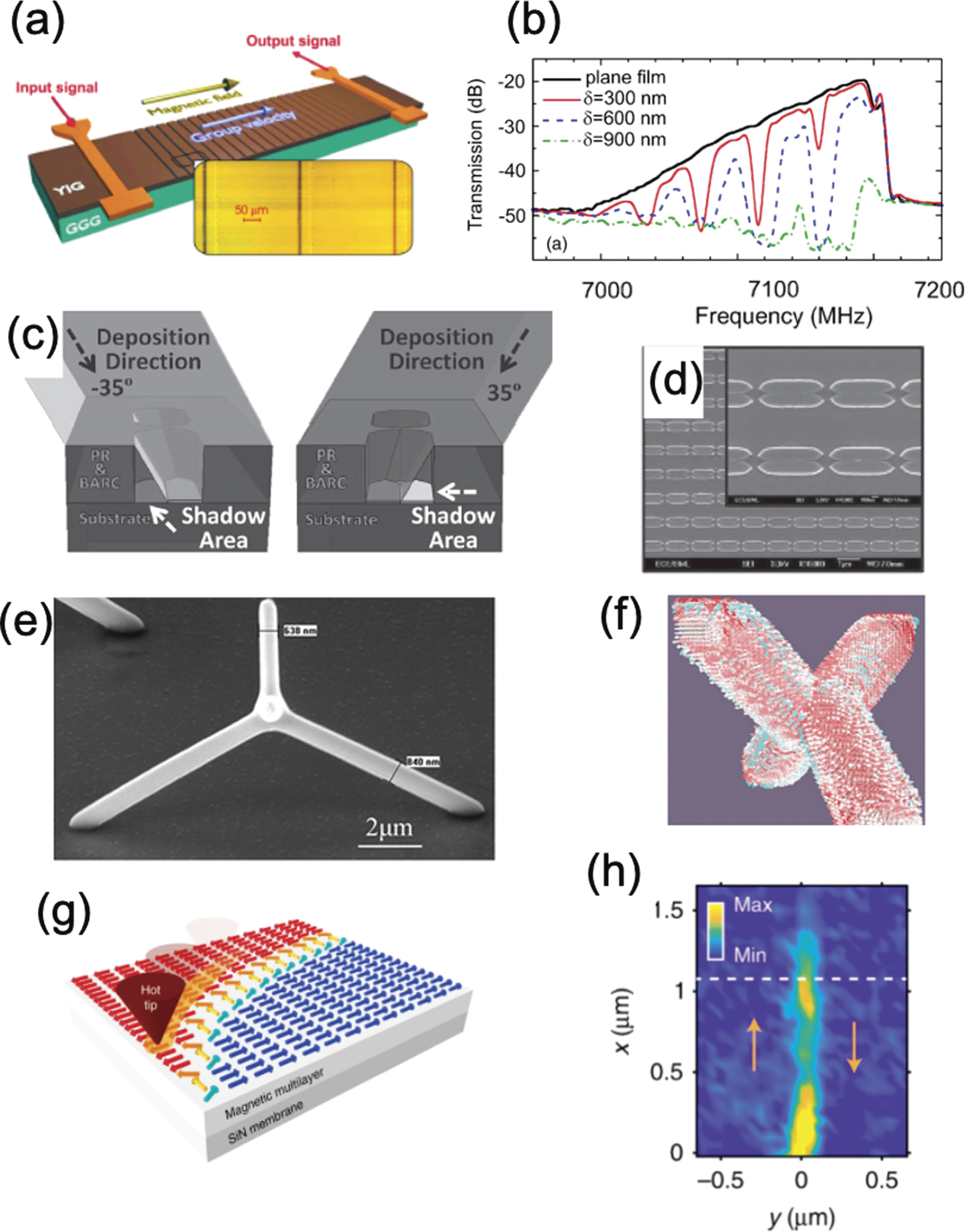
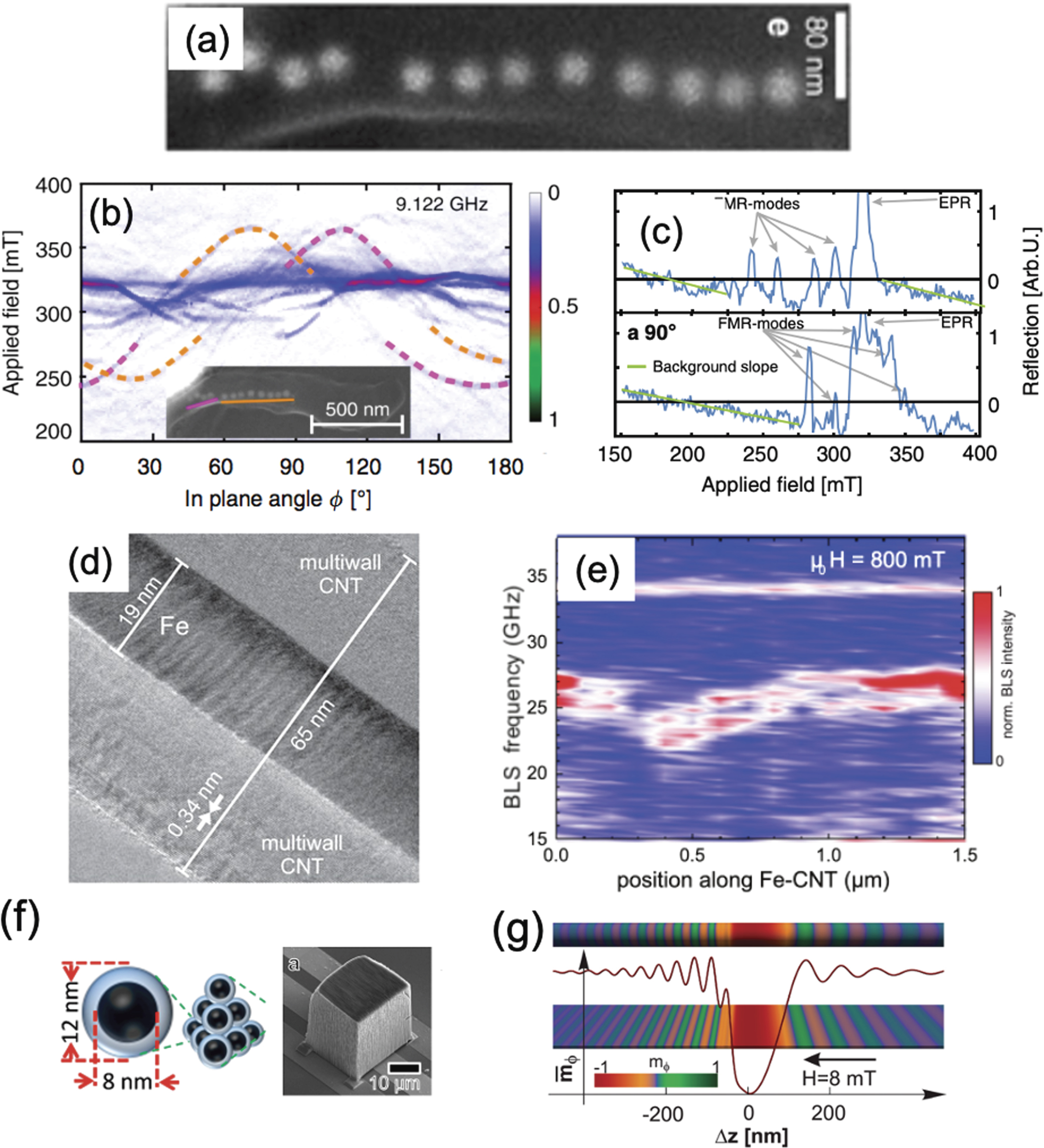
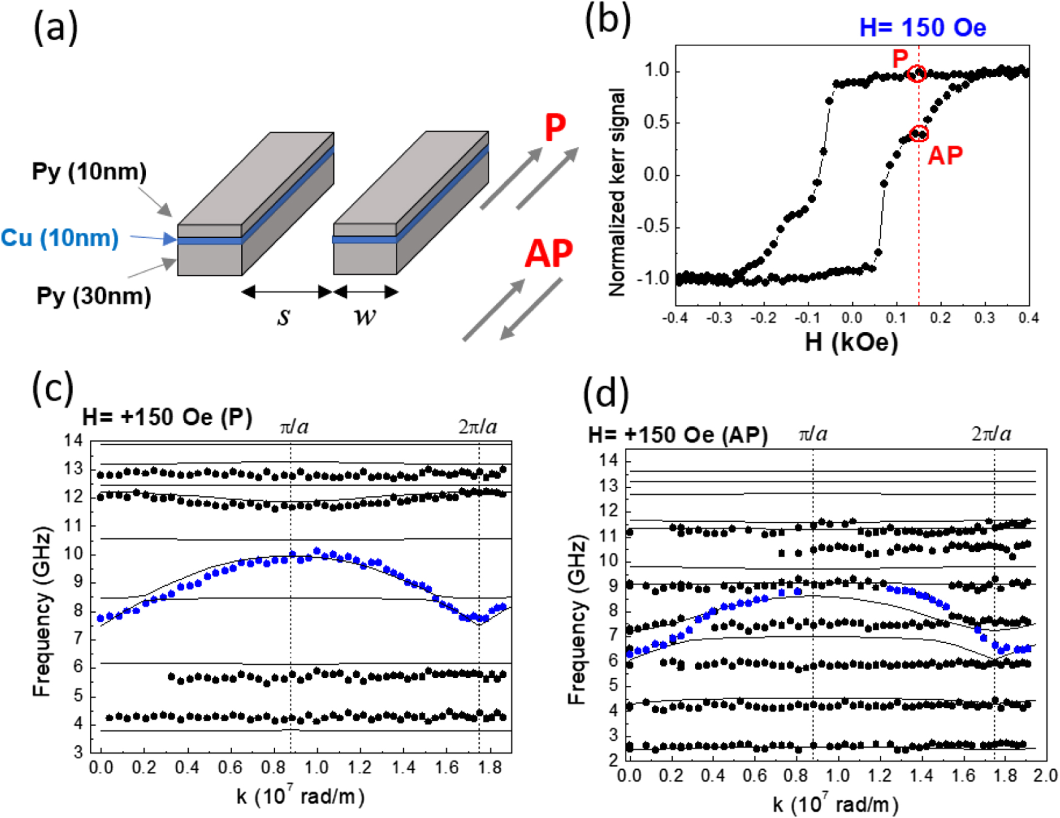
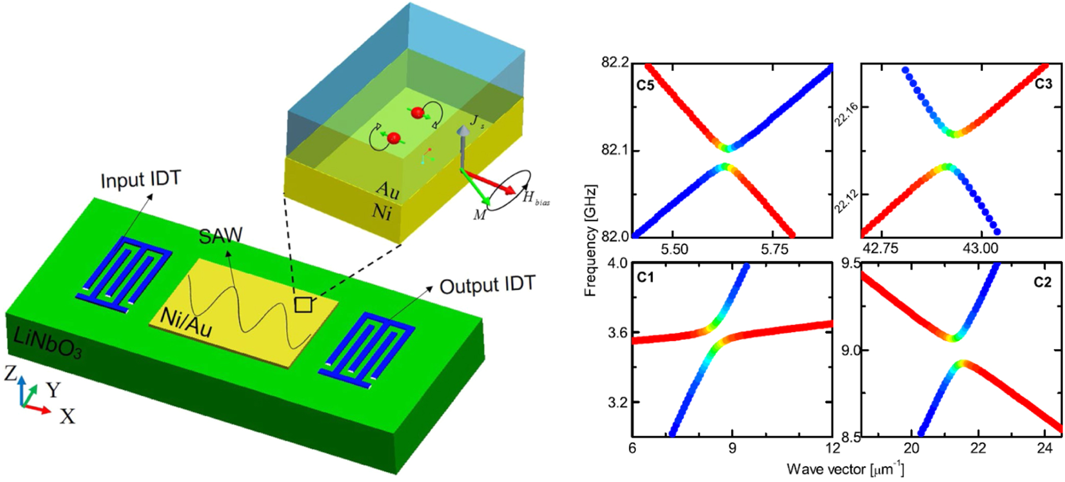
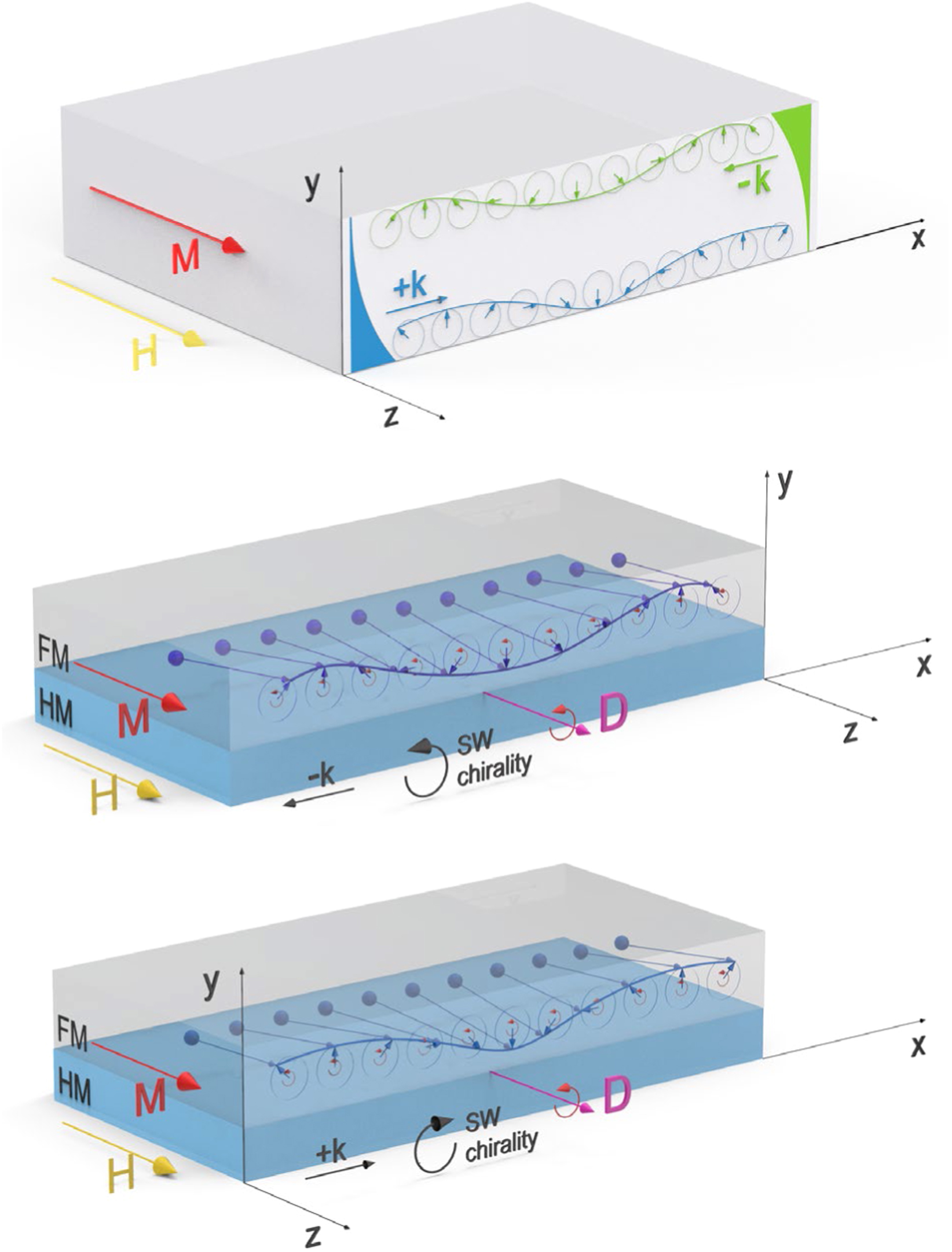
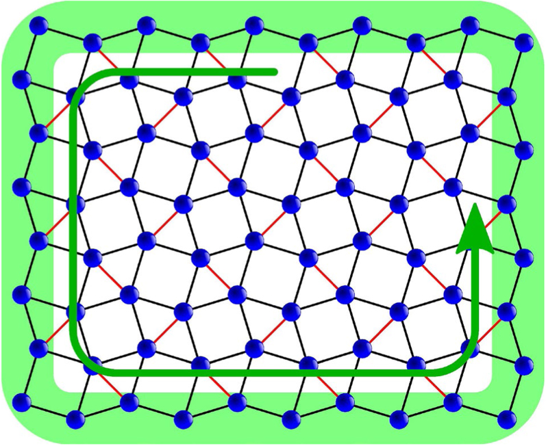
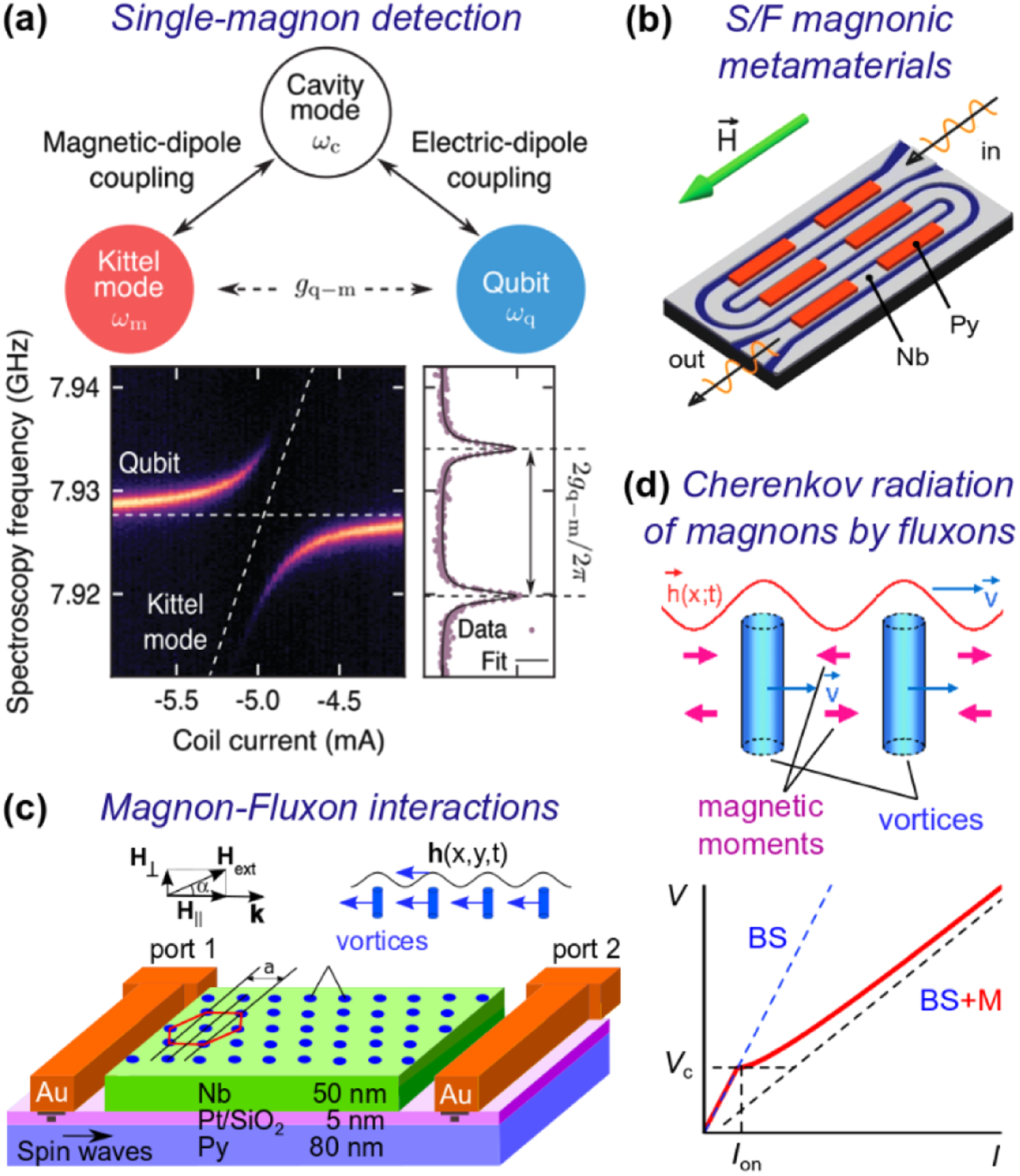
Figure 42. (a) and (b) Transmission electron micrographs of air-dried cells of wild type Magnetospirillum gryphiswaldense (a) versus ΔmamK mutant (b). The proportion of curved or dendritic particle arrangements (red highlights) is higher in the mutant compared to the wildtype in which mostly straight (blue highlights) chains occur. (c) Pictographic representation of desired development of suitable magnonic networks, from simple magnetosome (left) via suitable gate structures (center) to computational magnonic networks. (d) Moore's law for semiconductor electronics along with the transistor count in various CPU models. The blue marking (top right) indicates the estimated number of magnonic logic gates that could be accommodated in the volume of an 8-core Core i7 Haswell-E CPU, due to the obsolescence of heat sink material in magnonics computing. (a), (b) and (d) Reproduced from [254]. CC BY 4.0.
Download figure:
Standard image High-resolution image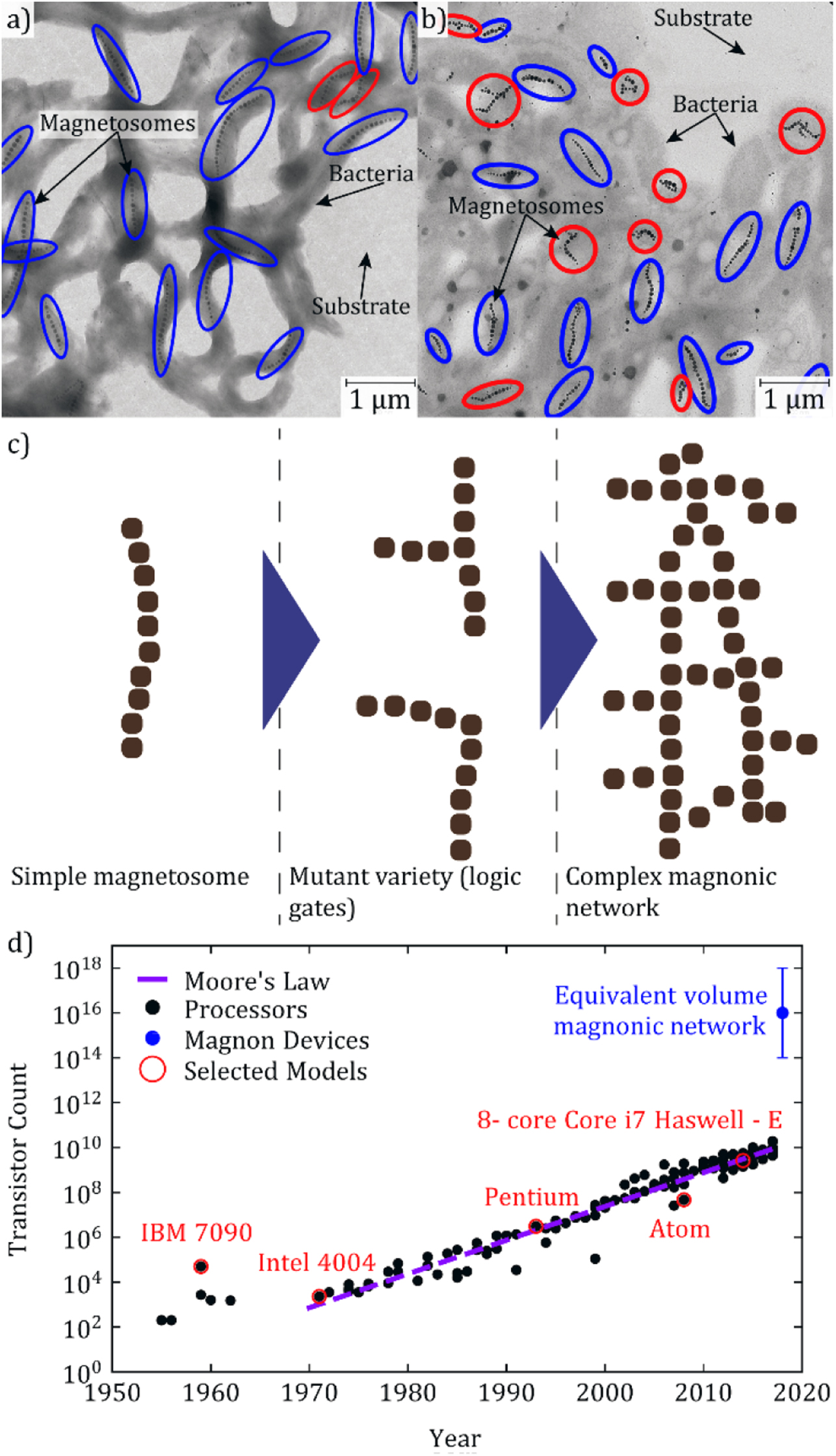
22.2. Current and future challenges
Thus far, we have studied single cells of just two genotypes. Still, there are many more species of magnetotactic bacteria to be explored in terms of their intrinsic magnonic properties and tailorability. Single-cell measurements will have to be guided and underpinned by micromagnetic simulations (e.g., figure 41) to identify candidate geometries for magnonic applications. The geometries may be produced lithographically and biologically, with biogenic production having two distinct advantages: first, the biological growth mechanisms ensure excellent crystallinity, magnetic single-domain character, consistent shape, and narrow particle-size spectrum [253]. Secondly, bacterial cells can be produced in large batches from which candidate cells with potential logic gates can be isolated, amplified, and perhaps even further optimized by directed evolution. Once a bacterium has been selected for desired magnonic properties, self-reproduction yields exponential production scalability. At the same time, it is essential to further advance our understanding of the molecular cell biology of magnetotactic bacteria to allow for targeted genetic engineering of desirable magnonic logic gates and even computational magnonic networks (as illustrated in figure 42(c)). Damping and other transport properties can be tailored through particle size and material choice. Although the composition of the magnetic material in magnetotactic bacteria is under genetic control and thus only partially influenceable during active growth [258], it is nevertheless amenable to post-growth modification. Thereby, logic gates can be tuned toward fast operation (large damping) and long transport distances (small damping) simultaneously.
Another challenge to nanomagnonics is the input/output periphery for spin-wave excitations on the nanoscale. One option to write individual inputs and read individual outputs is to drive the magnons through spin-torque excitations. This technique can be used for magnetic switching [260], but also for dynamic excitation of spin-wave normal modes [261]. The drawback of involving electrical currents can be mitigated by using a minimal amount of electrical inputs and outputs to an, otherwise, all-magnonic network.
22.3. Concluding remarks
The reachable density of logic gates when using networks of nano-sized magnon logic elements (e.g., figure 41) has the potential to outperform conventional charge-based silicon transistors (figure 42(d)). Self-organized magnonic gates can be harvested from magnetotactic bacteria (figure 42(b)), allowing for sustainable production of magnonic logic gates with exponential scalability. Future attempts will focus on engineering biological cells to produce magnetic nanoparticle configurations that perform desired magnonic tasks.
Acknowledgments
The authors thank Michael Farle, Ralf Meckenstock, and Thomas Feggeler who significantly contributed in acquiring the first ferromagnetic resonance spectra of individual magnetosomes. Both authors acknowledge financial funding by the Deutsche Forschungsgemeinschaft (DFG, German Research Foundation), BZ: Project-ID 405553726—TRR 270, MW: Project-ID 395940726—SFB 1372.
Data availability statement
All data is made available by the authors upon reasonable request.