

Abstract
We investigate the pure spin-current assisted depinning of magnetic domain walls in half ring based Py/Al lateral spin valve structures. Our optimized geometry incorporating a patterned notch in the detector electrode, directly below the Al spin conduit, provides a tailored pinning potential for a transverse domain wall and allows for a precise control over the magnetization configuration and as a result the domain wall pinning. Due to the patterned notch, we are able to study the depinning field as a function of the applied external field for certain applied current densities and observe a clear asymmetry for the two opposite field directions. Micromagnetic simulations show that this can be explained by the asymmetry of the pinning potential. By direct comparison of the calculated efficiencies for different external field and spin current directions, we are able to disentangle the different contributions from the spin transfer torque, Joule heating and the Oersted field. The observed high efficiency of the pure spin current induced spin transfer torque allows for a complete depinning of the domain wall at zero external field for a charge current density of  A m−2, which is attributed to the optimal control of the position of the domain wall.
Export citation and abstract BibTeX RIS
The lateral spin valve geometry has emerged as an attractive concept for spintronic devices, since it offers a convenient and effective means to study the transport properties of pure diffusive spin currents [1–3] and additionally has potential in applications such as future miniaturized magnetic read-heads [4]. Two ferromagnetic submicron electrodes are spatially separated but connected via a non-magnetic spin conduit which can be a metal or a semiconductor. A spin-polarized charge current flows from the first ferromagnetic electrode, the injector, to the conduit. This leads to a spin accumulation which diffuses away from the injection point as a pure spin current and reaches the detector ferromagnet. Here it can be detected by a voltage drop between the spin conduit and the detector electrode. Recently, it has been shown that pure spin currents can be employed to switch the magnetization state of small magnetic discs [3] and furthermore efficiently displace magnetic domain walls (DWs) via spin transfer torque [5–7]. To obtain reproducible domain wall displacements one needs well-defined spin structures with simple magnetization profiles, so that the acting torques are coherently displacing the wall. Hence, the uniform spin structure of a transverse domain wall is more appropriate than a vortex wall, where all magnetization directions are present [8]. Both in fundamental research and possible applications, a reproducible initial state is crucial to provide a repeatable device behaviour and to understand the underlying physics. Furthermore, it is necessary to be able to disentangle the contributing physical effects in order to obtain a full understanding of the device and the inherent efficiency of the pure spin current.
In this study we show that these two requirements can be fulfilled in a lateral spin valve device which employs geometrically tailored half rings as the ferromagnetic electrodes. We demonstrate that our geometry provides the required reproducible initial configuration for current-induced domain wall depinning due to the patterning of a constriction in the detector, which allows for a very precise control of the wall position and spin structure within the ring. In addition we study the field-induced depinning, observing a good agreement between experiment and micromagnetic simulations. By measuring the depinning field as a function of charge current density for various configurations of injector magnetization direction and spin current orientation, we are able to disentangle all different contributions to the effective torque acting on the domain wall.
Lateral spin valves with half ring geometry electrodes are fabricated by e-beam lithography and conventional lift-off techniques. In the first step, we patterned two half rings: one 100 nm wide (detector electrode) and the other 300 nm wide (injector electrode) with an edge-to-edge distance of 100 nm and then we deposited 30 nm of Py using UHV e-beam evaporation as shown in figure 1, "where we present SEM images of a typical device". For these widths, the energetically most favourable domain wall configuration for the detector is a transverse wall, although both transverse and vortex are stable configurations for this cross section. This is different for the injector, where a vortex wall is energetically favoured [9]. Since transverse walls are only stable for very narrow wires, the choice of geometries in particular for the wire width is restricted. One way to overcome this is to use notches to generate constrictions where transverse walls can be stabilized even for wires that are wider in the unconstricted part [8]. The half ring geometry is used since it facilitates the positioning of the DWs at desired angular locations within the structure [7] without needing to inject the walls from adjacent nucleation pads. Such pads can lead to a different device behaviour depending on the varying initialized domain wall spin structures which show more pronounced metastability in the wider regions of the device [10]. For half rings of constant width, the exact nucleation position of the walls is determined by local minima in the potential energy landscape due to defects and edge roughness. Furthermore, since the depinning fields for the two DWs are expected to be close to each other, it can be difficult to independently control the configuration of each ring. In order to overcome these limitations and to have a more robust device performance, we patterned a triangular notch in the narrow half ring to provide both a well-defined DW pinning potential and to promote the stability of the transverse domain wall (see figure 1(a)). Furthermore, for domain wall formation at the notch the nucleated spin structures are also expected to be robust due to the dominating influence of the geometry, removing a source of device asymmetry [11]. In the second step, in situ argon-ion milling is used to provide clean, oxide-free Py/Al interfaces and then a 90 nm thick and 100 nm wide Al wire is deposited as the spin current conduit (SCC), directly above the center of the half rings and thus above the notch in the detector.
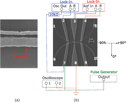
Figure 1. (a) Patterned Py half rings before the Al deposition with a 30 nm deep and 60 nm wide notch in the narrow half ring acting as an artificial pinning center for the transverse DW. (b) Scanning electron microscopy (SEM) image of the complete device with labeled contacts and used instruments for measuring the non-local signal and the current-induced depinning measurements. ±90° are the field directions for the depinning experiments, which are discussed in detail in the text.
Download figure:
Standard image High-resolution imageTransport measurements are performed at 4.2 K via a dual lock-in technique which enables the measurement of the precise DW motion in the vicinity of the SCC [7]. To confirm this, we first focus on a non-local Mode-Étoile measurement [7] where an external field of 150 mT is applied under an angle  in the range of
  and
and  with respect to the
  axis as defined in figure 1(b). For each angle, the external field is then consequently set to zero, thereby nucleating domain walls at the given angular positions in the rings. During this field sweep, a small probe current is applied via the lock-in amplifier between the injector and one end of the conduit (contacts 7 & 8), which generates a decaying spin accumulation in the conduit. A non-local signal is then measured as a voltage between the other end of the conduit and the detector (between contacts 2 & 3 or 3 & 4). Such a voltage arises due to the non-equilibrium shift in the chemical potential of the conduit with respect to the detector and thus depends on the relative alignment of the spins in the spin current and the magnetization direction in the small region where the spin current is absorbed. Since both the direction of the injected spins and the orientation of the absorbing magnetization change depending on the positioning of the domain walls in the injector and detector, respectively, careful analysis of the data allows us to probe the simultaneous motion of both the vortex and transverse wall as shown in figure 2. The blue curve is measured between contact 2 and contact 3, also called the half configuration, and probes the left part of the detector. The red curve (cross configuration) is measured between contact 3 and contact 4 and therefore is sensitive to the right part of detector [7]. In figure 2(a) we show the non-local signal with the complete parallel and antiparallel alignment of the magnetization of the two half rings where the non-local signal is defined by the ratio of the measured voltage drop and the applied charge current. Please note that the applied current density of
  A m−2 is too low to affect the signal. Furthermore, the non-local signal is shifted to 0 m
 in the case of a parallel magnetization alignment of the two electrodes with the offset for our samples being about 2.0 m
 . While the states I/I and VII/VII represent a parallel alignment of the half rings and therefore are trivial, all other levels correspond to different magnetization states and indicate a complex energy landscape. For the same device without a patterned notch you can find an analogous detailed analysis, including a complete discussion of the spin signal and the corresponding spin configuration of the DWs and position, in our previous work [7]. In this work we focus on the non-local levels II and V since for these non-local levels, the transverse wall is pinned inside the notch as shown in figure 3. The exact positioning of the transverse wall is one key requirement to perform the depinning measurements and can be reproducibly initialized only by the aid of the notch. As can be seen in figure 2, the angular range corresponding to the desired configurations II and V, while larger than in previous work [7], is still quite limited and was found to depend on the previous magnetic state of the sample. However for reliable device operation it is necessary to ensure that the vortex wall is reproducibly positioned away from the injection region in order that the injected spins are homogeneously oriented. This problem can be solved by applying an external field lower than 10 mT in the −90°-direction and lower than 17 mT for the +90°-direction. As later shown, these are the field values where the transverse wall depins for the respective field sweep direction. Since the vortex wall has a lower depinning field due to the absence of a strong pinning center, applying such fields and relaxing to zero provides a robust path to achieve a homogeneously magnetized injector in the vicinity of the spin current conduit while ensuring that the transverse wall is still pinned inside the notch. As an additional advantage, the resulting spatial separation of the two domain walls means that dipolar-coupling between the two walls is minimized. Furthermore, for the subsequent depinning measurements, the injector magnetization under the conduit will remain constant and parallel to the direction of the external field. This simplifies the analysis significantly because all changes in the non-local signal must then occur due to the motion of the transverse wall.
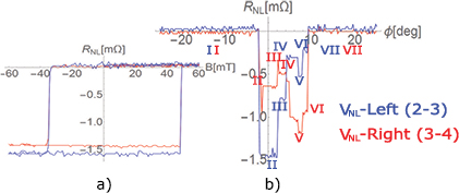
Figure 2. Non-local signals for the half and cross configuration as a function of the external field parallel to the rings. The two states correspond to the full switching between the parallel and antiparallel magnetization alignment of the two half rings with the signal of the parallel alignment shifted to 0 m . (b) Non-local Mode-Étoile measurement which is sensitive to the motion of both DWs within the half rings and the corresponding non-local inside. We are interested in those levels where the transverse wall is pinned inside the notch as one key requirement for the depinning experiments which are explained later in detail.
Download figure:
Standard image High-resolution image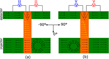
Figure 3. Schematic illustration of the DW configurations with the transverse wall pinned inside the notch which correspond to the non-local levels II/II and V/V. To reduce the dipolar-coupling between the two walls, a small external field is applied before starting the depinning experiments in order to depin the vortex wall from the vicinity of the notch while keeping the transverse wall pinned inside the notch.
Download figure:
Standard image High-resolution imageTo further investigate the nature of the domain wall pinning potential, we carry out field induced depinning measurements as presented in figure 4(a). A clear asymmetry in the behaviour is observed, with two depinning events seen for negative sweeps at fields of −10 mT and −28 mT, whilst for positive field sweeps just one depinning event is seen at a field of +17 mT. Since the domain wall initialization procedure always generates the domain wall at the same position inside the notch, such asymmetries are expected to reflect the intrinsic potential landscape and not variations in the initial domain wall spin structure or position with respect to the notch which have been the cause of asymmetries in other studies on straight wires [10, 11]. As such this is an important result since it shows that we probe the asymmetric potential landscape of the domain wall in the vicinity of the notch with the depinning fields being a measure of the energy barrier that the DW has to overcome to be depinned [12]. In order to understand the surprising asymmetry in the experimental results in more detail, micromagnetic simulations were performed with a finite difference solver [13]. The shape of the simulated sample was extracted directly from the SEM image shown in figure 1(a) and used as input for the solver, leading to a realistic edge roughness profile and notch configuration, as shown in figure 4(b). In this way the magnetization dynamics were simulated over an arc of the ring with a radius of 5 μm, 100 nm width and 30 nm thickness. To perform the simulation, standard values for the material parameters of Py were used:  A m−1,
  J m−1 for the saturation magnetization and exchange constant, respectively. An arc of the ring of 36° was simulated, corresponding to a simulation box of
  nm3 discretized in cells of
  nm3. The initial configuration was then obtained by first saturating the sample along the
  -direction and relaxing the magnetization to obtain a transverse head-to-head DW pinned below the notch. Next, the depinning field was extracted for both positive and negative sweep directions by calculating the sequence of equilibrium configurations for increasing field amplitudes in steps of 0.5 mT. In order to magnify the variations of the
  -value corresponding to DW movements, the x-component of the average magnetization was extracted from a 768 nm wide region with the notch in the center. We observe that edge roughness gives rise to an asymmetric energy landscape for the DW, resulting in a different depinning behaviour depending on the direction of the applied field as shown in figure 4(b). As in the experiment, we observe a different number of jumps for the two external field sweep directions: For the negative field sweep direction, we observe four distinct jumps at −9, −15, −20.5, and −36.5 mT. These jumps are caused by the movement of the DW between different pinned positions below the notch that are induced by edge roughness defects. The jumps associated with the jumps in the experimentally observed non-local signal of figure 4(a) are the ones at −15 mT, where the DW changes its internal structure to a vortex wall, and at −36.5 mT where the DW completely depins and leaves the sampled area. Please note that the jumps at −9 mT and at −20.5 mT, where the DW keeps its internal structure within the sampled area, are not detected in the experiment. For external fields applied along the +90°-direction, only one jump is observed at 31 mT which corresponds to the complete depinning of the DW. This is caused by the pinning site configuration which strongly pins the DW for applied fields in the positive direction. The simulations reveal that in realistic systems with edge roughness, transformations from vortex to transverse walls can occur during DW propagation, even when the transverse wall would be expected to be energetically stable for the given nominal width. This is disadvantageous for domain wall displacement via spin-currents, since the torque on the wall depends on the alignment of the spin current and the absorbing magnetization. However, our incorporation of a strong geometrical pinning potential at the conduit position provides a robust way to set or reset a reproducible transverse wall configuration at this position, even for the case when a vortex wall is stable in other parts of the wire. In this first step we have characterized the energy potential landscape generated by the notch using purely field induced depinning, where the spin current merely provided a signal to detect the domain wall displacement.

Figure 4. (a) Field-induced non-local depinning measurement at 4.2 K with the signal normalized to the parallel alignment. The jumps correspond to depinning and spin structure transformation events. (b) Micromagnetic simulation for 0 K of field-induced DW motion. Starting with the wall pinned at the notch (i), for a positive field depinning takes places at 31 mT (iii), whereas for negative fields the wall is first transformed into a vortex configuration at −15 mT (v), and finally depinned from the notch at −36.5 mT (vi).
Download figure:
Standard image High-resolution imageNow we turn our attention to the functionalization of the spin current and investigate its ability to itself displace the domain wall. By taking advantage of the measurement schemes afforded by the geometry, we are able to distinguish different contributions to the spin torque on the domain wall. To investigate the efficiency of the pure spin current in displacing the domain wall we measure the change in the depinning field of the wall as a function of current density as follows: Firstly, we apply a short current pulse between contact 7 and contact 8 in the injector. Secondly, we increase the external field by an increment of 0.25 mT and thirdly, we measure the non-local signal with the lock-in-amplifier. These three steps are repeated until the transverse wall is completely depinned, which can be identified by a jump in the non-local signal. This means that now the non-local signal is no longer measured at remanence since the transverse wall stays pinned at 0 mT due to the notch. Please note that due to a long pause between applying the current pulse and increasing the external field, the measurement is quasi-static. The current density is calculated from the applied pulse voltage, divided by the average increase of the resistance between contact 7 and contact 8 of the injector during the pulse which is measured by the oscilloscope.
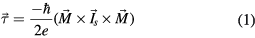
In contrast to field induced experiments where the displacement of the domain wall is governed simply by the precessional and damping torques from that applied field, for current induced experiments there are several effects which can all influence the measured depinning fields. The first we consider is the spin transfer torque which is given by [14, 15]
where  is the magnetization of the DW and
  is the pure spin current. The sign of the spin transfer torque depends on the polarization of the pure spin current (which can be controlled by the current pulse direction) and the injector magnetization direction. As previously mentioned, the injector magnetization stays parallel to the external field sweep direction during the whole measurement. If the injector magnetization and the spin current polarization are aligned parallel, the spin transfer torque will assist the external field to depin the domain wall while for an antiparallel alignment, the spin transfer torque impedes the depinning. Joule heating, caused by applying high current density pulses, is independent of the pulse direction and the injector magnetization direction and scales quadratically with the applied current density of the pulse. A last possible contribution is the Oersted field, generated by the current, which changes its sign on changing the current direction but is independent of the injector magnetization direction. By measuring the depinning field as a function of the applied current density for the different current and injector magnetization directions, we are able to disentangle the three contributions to the depinning field. To this end, we investigate the depinning field as a function of the charge current density for the two external field sweep directions. The depinning field is defined as the external field value where the jump in the non-local signal occurs and the error bars are determined by the chosen step size of 0.25 mT and statistical fluctuations in the depinning field [16]. The depinning efficiencies, defined as the slopes of the decrease in the depinning field as a function of the charge current density, are summarized in table 1. In addition, we show representative curves for cases where the spin transfer torque supports the external field in figure 5. For the two sweep directions, we notice a different behaviour of the depinning field as a function of the current density which can be explained by the different energy landscape of the domain wall depending on the sweep direction. Although we observe a different depinning behaviour for the two sweep directions, we nevertheless find the same depinning efficiency for both curves. We are even able to completely depin the DW for current densities higher than 6 · 1011 A m−2. Since the Oersted field, Joule heating and the spin transfer depend differently on the spin current direction and injector magnetization direction, we are able to disentangle the contributions through a comparison of the different efficiencies [17].
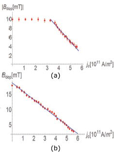
Figure 5. Depinning field for the first jump as a function of the current density for the negative (a) and positive (b) field sweep direction with an equal depinning efficiency for both sweep directions in the case of parallel alignment of external field and spin direction of the spin current.
Download figure:
Standard image High-resolution image
Table 1. Overview of the efficiencies (in 10−11 mT · m2 A−1) for the two different field sweep directions and for the parallel and the antiparallel alignment between spin current orientation and injector magnetization direction.
| Alignment | Sweep direction | First jump | Second jump |
|---|---|---|---|
| Parallel | − | 2.82 ± 0.08 | 1.29 ± 0.04 |
| + | 2.78 ± 0.04 | n/a | |
| Antiparallel | − | 0.86 ± 0.04 | 1.25 ± 0.22 |
| + | 2.12 ± 0.08 | n/a |
Firstly, we consider the first depinning event for the case of parallel alignment. Here the spin transfer torque supports the external field, but the current direction and hence the Oersted field is reversed for the two sweep directions due to the different device configurations in each case (see figure 3). Furthermore, since the Joule heating will also be identical for these two cases, any difference can only occur due to an Oersted field. As can be seen from the table, the efficiencies in these two cases are identical within errors and hence any Oersted field contribution is negligible. The vanishing in-plane Oersted field is consistent with expectations of calculations from the Biot–Savart law, which leads to an out-of-plane field of about 2 mT and to a negligible in-plane field which is also easily demonstrated in straightforward COMSOL calculations.
Next, we consider the spin transfer torque efficiency. For a given sweep direction, the spin transfer torque contribution reverses on reversing the alignment, but the Joule heating contribution remains constant. Hence, given the vanishing Oersted field contribution deduced above, the spin transfer torque can be calculated from the average of the difference in the pairs of slopes. For the negative sweep direction this yields 0.98 · 10−11 mT  m2 A−1 and for the positive direction 0.33 · 10−11 mT · m2 A−1. These values are lower compared to previous studies [7] and vary considerably for the two cases. However, the simple image of a spin current easily acting in the exact opposite direction to the applied field is an oversimplification, even in the case of transverse walls which nevertheless have a simpler spin structure than vortex walls. The exact torque is expected to depend very precisely on the location of the DW with respect to the conduit, the width of the conduit and the exact shape of the domain wall whereas the Joule heating and Oersted field are expected to act much less locally. This actually provides an independent means to estimate the Joule heating efficiency, since for the second jump observed for the negative sweep direction the DW has already moved away from the central region. Due to the short spin diffusion length in Py, [18] the spin current is absorbed directly and therefore Joule heating should dominate in this case. From the average of the two efficiencies for the second jump we conclude that the Joule heating efficiency is 1.27 · 10−11 mT · m2 A−1. Finally this allows us to calculate a corrected spin transfer torque efficiency of 1.53 · 10−11 mT · m2 A−1 by the subtraction of the overall efficiency and the efficiency determined for the Joule heating. The summarized efficiencies are shown below:


Here, estt is the calculated efficiency of the spin transfer torque, eJh the effiency of the Joule heating and eOf the efficiency of the Oersted field.
The calculated efficiencies show that while Joule heating is still an important contribution to the thermally activated domain wall depinning, the spin transfer torque accompanying the absorption of the pure spin current is a significant dominant effect even in the case of relatively strong geometrically defined pinning potentials. This high efficiency bodes well for the employment of such pure spin currents in future devices where the DW position and spin structure are tailored and constructed by strategically placed constrictions in the structure.
In conclusion, we studied spin current-assisted depinning in Py/Al lateral spin valves at 4.2 K where a notch is patterned in the narrow Py half ring, the detector. This notch acts as an artificial pinning center for the DW and allows for the precise positioning of the DW within the half ring. We demonstrate that using the DW pinning, we can obtain a robust spin configuration with variable injector magnetization as determined in Mode-Étoile measurements. This allows us to study field-induced domain wall depinning for the two field sweep directions. For the field-induced motion, we observe both in the experiment and in micromagnetic simulations an asymmetry between the two field sweep directions indicating that we probe the potential landscape of the domain wall in the vicinity of the notch. By exploiting the symmetries of the different acting effects and using the flexibility and robustness of the spin configurations, we are able to determine the influence of Joule heating, spin transfer torque and Oersted field separately. The Oersted field is found to be negligible in our devices, while the spin transfer torque and Joule heating are of the same order of magnitude. Finally we are able to depin a DW completely just by applying a current pulse with a charge current density of 6·1011 A m−2 even in a system with strong pinning potential, demonstrating that our geometry is convenient for efficient domain wall displacement and at the same time allows for stable domain wall positions as needed for applications.
Acknowledgments
This work was funded by the German Ministry for Education and Science (BMBF), the German Research Foundation (DFG) via the DFG collaborative research centre SFB/TRR 173 SPIN+X, the Graduate School Material Science in Mainz (DFG/GSC 266), EU 7th Framework Programme (WALL FP7-PEOPLE-2013-ITN 608031; MAGWIRE, FP7-ICT-2009-5), the European Research Council (MultiRev 665672) and the Research Center of Innovative and Emerging Materials at Johannes Gutenberg University (CINEMA). A Pfeiffer and M Kläui thank the participants of SpinMechanics 2 Workshop for valuable discussions and are grateful for financial support from the German Academic Exchange Service (DAAD) via the SpinNet Program (56268455). The device were fabricated in the Plateforme Technologie Amont in Grenoble, for which a support from the French RENATECH network is acknowledged. LL-D acknowledges the support by Project MAT2014-52477-C5-4-P from the Spanish government and Project SA090U16 from Junta de Castilla y Leon.