
Abstract
Solid state physics (SSP) research at ISOLDE has been running since the mid-1970s and accounts for about 10%–15% of the overall physics programme. ISOLDE is the world flagship for the on-line production of exotic radioactive isotopes, with high yields, high elemental selectivity and isotopic purity. Consequently, it hosts a panoply of state-of-the-art nuclear techniques which apply nuclear methods to research on life sciences, material science and bio-chemical physics. The ease of detecting radioactivity—<1 ppm concentrations—is one of the features which distinguishes the use of radioisotopes for materials science research. The manner in which nuclear momenta of excited nuclear states interact with their local electronic and magnetic environment, or how charged emitted particles interact with the crystalline lattices allow the determination of the location, its action and the role of the selected impurity element at the nanoscopic state. ISOLDE offers an unrivalled range of available radioactive elements and this is attracting an increasing user community in the field of nuclear SSP research and brings together a community of materials scientists and specialists in nuclear solid state techniques. This article describes the current status of this programme along with recent illustrative results, predicting a bright future for these unique research methods and collaborations.
Export citation and abstract BibTeX RIS

Original content from this work may be used under the terms of the Creative Commons Attribution 3.0 licence. Any further distribution of this work must maintain attribution to the author(s) and the title of the work, journal citation and DOI.
Introduction to the solid state physics (SSP) programme at ISOLDE
The quality and intensity of radioactive beams available at ISOLDE have long attracted interest from researchers beyond the core nuclear physics community, and have formed an extremely active programme in 'applied nuclear physics' since the late 1970s. A different set of criteria exist for the successful application of radioactive beams to other domains. The properties of the isotopes which are applied to a secondary area are well understood as properties such as the half-life and decay characteristics are harnessed in the study. The intensity of the beam is typically quite strong: as a guideline, a minimum of 107 particles per second is required. With such an intensity, implantations into matrices achieve the required activity within a timeframe of several seconds to 3–4 h. The applied programme at ISOLDE embraces biology, medicine and SSP and typically accounts for about 15%–20% of the annual physics schedule, as seen in figure 1; although the overall percentage has remained relatively constant over the years, increased intensities of beams has allowed for an increase in the number of experiments in this domain, which now accounts for about 20%–25% of the overall number of running experiments at ISOLDE.

Figure 1. Distribution of experimental areas at ISOLDE since 1998. As can be seen, the solid state programme averages around 10%–15% of the yearly allocation of beam time.
Download figure:
Standard image High-resolution imageThis article will describe the SSP programme at ISOLDE; biology and other applied aspects of the scientific programme being described in separate articles in this volume. Referring again to figure 1 we see that the solid state programme is a considerable percentage of the programme, a feature which is unique to ISOLDE among the large scale nuclear facilities in Europe. The only other facility worldwide which allots a similar amount of experimental time to SSP is TRIUMF in Canada where the β-NMR experiments enjoy a similarly privileged position [1]. This is mostly due to the inherent flexibility of the ISOLDE machine where SSP can either run in parallel or be relatively easily accommodated along with dedicated nuclear physics experiments. The GPS separator is especially favourable for these experiments: the mass resolution of M/ΔM = 2400 for 20 mm mrad beams is sufficient for applications and the low and high mass beamlines can be utilised to deliver beams to within a mass range of ±15%. The main factor behind the strong showing of the solid state programme at ISOLDE has been the continued investment in infrastructure by a number of funding agencies over the past 20 years. In particular, the role of the German BMBF in delivering support for experimental equipment and manpower has allowed the development of on-site laboratories removing the need to transport radioactive samples back to home institutes for the majority of experiments while also allowing the community to apply ever-more exotic isotopes to SSP. In addition to the BMBF support, sustained investment from the Portuguese FCT and Belgian (FWO) in collaboration with the University of Leuven (KU Leuven) have allowed a considerable suite of labs and instruments to be put in place which offer the opportunity for unique experimental programmes to be pursued, these will be discussed further in the perspectives section at the end of the article. At the time of writing, there were 25 active experiments in the field of solid state research at ISOLDE.
Radioactive ions in SSP research
Almost all experiments that apply radioactivity to materials follow the same procedure: the activity is introduced to the material usually by implantation or diffusion and the effect of the implanted isotope is then studied within the host, utilising either one or both of the key properties of the implanted isotopes: its half-life and/or decay properties. The application of radioactivity to SSP has itself a long history, dating back to the original work of de Hevesy who utilised radioactive Pb atoms to investigate self-diffusion in Pb [2]. De Hevesy's work formed the basis for radiotracer diffusion, the essence of which has not changed since the early 1920s. The discovery of the Mössbauer effect (ME) in 1957 [3] was soon applied to the field of SSP and magnetic materials in particular [4]. Perturbed angular correlation (PAC) experiments emerged from nuclear physics to be applied to SSP in the early 1970s [5] and channelling experiments—where the location of implanted isotopes can be described to high precision in the host lattice—were first performed with α-particles and electrons in the mid-1960s [6, 7]. All of the above techniques found a welcome home at ISOLDE and have continued to be practised to the present day. Some of the above—in particular, emission channelling—are almost unique to ISOLDE as without the availability of a wide variety of beams their relevance is lost. ISOLDE has also played a considerable role in the extension of radiotracer methods to 'classical' semiconductor spectroscopies. Of especial note have been the development of dedicated instruments for optical and electrical studies of impurities in semiconductors overcoming otherwise chemically blind methods [8, 9].
The choice of the radioactive ion will depend on its availability, purity, chemical nature and also its decay properties. The location of the ion in the target lattice is of crucial importance: this can be controlled by consideration of the chemical properties of the ion and also through post-implantation processes such as annealing. The wide number of beams available at ISOLDE also offers further choices—especially for radiotracer techniques—in terms of half-lives. For half-lives which exceed 2–3 d, systematic studies on the implanted sample are possible e.g. annealing sequences can be performed with great precision and control. In addition, such implanted samples can be shipped to home institutes—or specialist laboratories—where well-understood or familiar equipment can be used. However, increasingly there are restrictions in the number of laboratories which can routinely handle quasi-open radioactive sources, and such demands for long-lived activity has been decreasing in recent years. For isotopes with half-lives of the order of hours, it is usually only possible to make 1–2 measurements per sample before a new implantation is required. Although limiting in terms of systematic studies, the wider number of suitable probes available allows for considerable flexibility in the type of measurements possible. For probes with half-lives of the order of 1–10 min, it is necessary to perform measurements online. This puts considerable constraints on the type of post-implantation treatment which is possible, but again offers a wider variety of probes.
In the following sections, an overview of the various techniques and infrastructure which exists at ISOLDE will be presented. An exhaustive review of results for each individual technique will not be given, rather recent highlights and developments will better serve to describe the current state of the art.
Experimental techniques and results
Hyperfine interactions
Experiments, which measure hyperfine parameters account for the bulk of SSP experiments, carried out at ISOLDE viz. the ME and PACs. With these techniques, the radioactive nuclei are used as atomic scale probes in matter.
By emitting a specific decay particle or by just having excited states with the right spin and nuclear moments, radioactive isotopes overcome the limitations of ground states and stable nuclei. In the following sections, we briefly introduce the decay properties required for each technique. Hyperfine techniques (ME and PAC) rely on the interaction of the nuclear states, quadrupole and magnetic moments, with the electron density, electric field gradient (EFG) and magnetic hyperfine fields at the probe's location. By probing this information, they provide atomic scale information on defect structure, defect dynamics and electronic configuration. The EFG, in particular, provides information on the local charge density distribution and acts as a fingerprint of a specific defect trapped by the probe nuclei. These techniques are also used complementarily, e.g., while isomer and chemical shifts are only measured with ME, conversion electron (e−) and/or γ-ray PAC is essentially temperature independent and a wider range of probe nuclei can be used. A wide variety of beams suitable for hyperfine interactions are available at ISOLDE; they are summarized graphically in figure 2.

Figure 2. Periodic table highlighting elements produced as primary beams at ISOLDE for hyperfine interactions methods. Elements that have isotopes, which are adequate for applied research at ISOLDE are shown in green, blue and red. Yellow triangles define the direction of the decay for non-isomeric states and 'b–n' quotes for isotopes that are suitable for β-NMR measurements.
Download figure:
Standard image High-resolution imageMössbauer spectroscopy (MS)
MS is not only the oldest hyperfine technique applied to SSP but also the most widely adopted throughout the world. This is by virtue of the well-known 57Fe isomeric state which has a gamma transition energy of 14.4 keV with a lifetime of 142 ns, and which can be excited from the decay of 57Co (t1/2 = 271 d), which makes it an attractive option for laboratories around the world. In addition, the fact that 2.2% of the isotopic composition of natural iron is made of 57Fe, further guarantees that 57Fe/57Co Mössbauer experiments remain dominant in applied materials research, due to the isomeric shift which makes ME sensitive to the valence state of the probe atom, and also due to the importance of Fe in materials. MS can be executed in either absorption or emission configurations. In absorption spectroscopy the sample under study is doped with Mössbauer probe atoms in their ground states Ig. The γ-quanta emitted by a standard MS source outside the sample are absorbed in resonance by the probe atoms in the sample, converting the nuclear states from ground level Ig into the excited level Ii. Although this MS technique is very common, its sensitivity is much lower than in the case of emission spectroscopy and it is not the approach typically followed at ISOLDE. In emission spectroscopy, the samples under study are doped with MS probe atoms in their excited states. The γ-quanta emitted by the radioactive decay from the isomeric state of the MS probe atom into the ground state are analysed against a standard absorber which contains the MS probe atoms in their ground state in a non-magnetic environment with cubic symmetry (i.e. no EFG is present).
ISOLDE has been home to an extremely active Mössbauer programme since the late 1970s. The pioneer of this work was Weyer et al [10] who first exploited strong beams of 119In (t1/2 = 2.1 m) which then decay to the 24 keV Mössbauer state of 119Sn. Yields of about 5.108 In+ s−1 were possible at this time allowing for the successful production of 10 mCi sources within several minutes [11]. Among notable early results were studies of the structure and electronic states of impurity–vacancy complexes in III–V semiconductors and of Sb doping of Si-based semiconductors such as SiGe alloys, using the first excited state at 24 keV in 119 Sn, obtained via the aforementioned 119In decay or by 119Sb (38.2 h) [12]. Such studies were then extended to the wide band gap GaN semiconductor, by implanting 119Cs which decays through the 119Xe → 119I → 119Te →119Sb isobaric chain to the Mössbauer 119Sn nucleus. As the recoil energies are large during this decay (typically >50 eV) the 119Sb can be displaced onto both Ga and N sites which allows for the measurement of isomer shifts of Sn—acting as a donor or acceptor, respectively—on both Ga and N sites [13]. A more complete overview of earlier results can be found in Weyer [14].
The Mössbauer program at ISOLDE received a considerable boost in 1996 with the development of extremely pure and intense Mn beams, ionized using the then relatively new resonant ionization laser ion source (RILIS) ion source [15]. This allowed the exploitation of the short-lived 57Mn mother to produce strong sources of  the Mössbauer isotope par excellence. In comparison to standard
  Mössbauer studies—which typically use long-lived 57 Co sources, both in absorption and emission mode—the short half-life of 57 Mn in combination with the high purity-high-intensity beam available at ISOLDE (up to 2 × 10⁸ at s−1) allows for several orders of magnitude faster data acquisition, making it possible to record hundreds of Mössbauer spectra per day. The strength and purity of the Mn beam at ISOLDE is orders of magnitude greater than that offered by only other large scale facility lending a considerable advantage to the Mössbauer programme at ISOLDE.
The experimental setup for emission MS at ISOLDE consists of a resonance detector, which is used to detect the conversion electrons from the 14.4 keV of the 57Fe Mössbauer transition, as shown in figure 3. It is not feasible to detect a single low-energy conversion electron, so the resonance detector is equipped with a parallel plate avalanche detector [16] to amplify the signal. Across a ∼2 mm gap of the parallel absorber and collector there is a potential of ∼1 keV and a suitable counter gas (here ∼25 mbar of acetone gas). When an electron enters the gap it is accelerated by the potential, causing an ionization of the gas molecules, and an avalanche is detected.
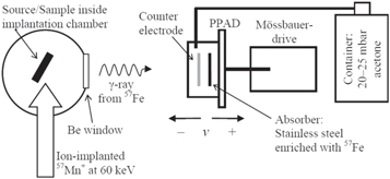
Figure 3. Schematic of the 57Fe emission Mössbauer spectroscopy setup at ISODLE/CERN for 57Mn ion implantation. The sample is implanted inside a vacuum chamber. The γ-rays pass through a 6 mm Beryllium window and are detected in the moving resonance detector. Ion implantation is performed at an incident angle of 30° relative to the sample surface normal.
Download figure:
Standard image High-resolution imageAlthough 57Mn/Fe remains the workhorse isotope for MS at ISOLDE, in recent years several other isotopes have been used. Recent developments with RILIS have allowed the resumption of the 119In/119Sn experiments and a programme utilizing other less common isotopes such as 151Eu and 197Au (with particular application to biophysics) has been underway for a number of years. These isotopes are summarized in table 1.
Table 1. Isotopes recently used in the Mössbauer programme at ISOLDE. Yields shown are measured except for those which are estimated (marked by ?).
| Isotope | Parent | Half-life | Maximum recoil | Detector | Target/ion source | Yields (s−1) |
|---|---|---|---|---|---|---|
| 57Fe | 57Mn 
|
1.5 min | 93 eV | Res. | UCx/RILIS | few × 108 |
| 57Co (EC) | 272 d | 0.14 eV | Res. | ZrO/VADIS | ∼107 | |
| 119Sn | 119In 
|
2.1 min | 22 eV | Res. | UCx/RILIS | ∼109 |
| 119mSn (IT) | 291 d | ∼0 eV | Res. | UCx/RILIS | ∼109 (?) | |
119Ag 
|
2.1 s | 102 eV | Res. | UCx/RILIS | ∼few × 107 | |
→119Cd  →119In →119In 
|
2.2 min | |||||
| 2.4 min | ||||||
| 197Au | 197Hg (EC) | 64 h | ∼0 | Ge | Pb | ∼109 |
| 151Eu | 151Dy (EC) | 17.9 min | ∼0 | Ge | Ta | ∼109 |
| →151Tb (EC) | 17.6 h | |||||
| →151Gd (EC) | 123.9 d |
Representative results from MS
The Mössbauer programme at ISOLDE is extensive and cannot easily be summarized within a short article such as this. Two examples will demonstrate the power of the emission Mössbauer technique to reveal unique aspects of problems which are not easily addressable by other spectroscopies.
The first of these concerns the role of Fe in Si. This is among the most deleterious of all impurities in devices and has been the focus of study for more than 60 years of research into Si materials [17]. In spite of this, many aspects of Fe in Si proved difficult to understand. MS helped to clarify not only the well-known interstitial Fe impurity, but also was among the first spectroscopies to study substitutional Fe, which had remained unstudied for much longer [18]. Interstitial Fe is known to exist in two charge states and other methods had been unable to pin down the dependence of the diffusivity of the well-known Fe+/0 charge states for the donor level which is at 0.38 eV above the valance band [17]. MS had measured the diffusivity of interstitial 57Fei which had been determined by in-beam experiments by the line broadening caused by diffusional jumps during the lifetime of the Mössbauer state [19]. Gunnlaugsson et al noticed that at temperatures above 500 K there was a clear broadening visible in the lines attributed to Fei [20], which was attributed to the diffusion of Fe during the Mössbauer lifetime. Accurate measurements clearly reveal that diffusion is faster for Fe+ than neutral Fe0. The relevance of these important data can be reflected in the fact that Si-based solar cells—still the bulk share of the worldwide market—need to control the influence of Fei to a very high degree with Fe needing to be 'confined' to a tolerance of only 1012 cm−3 in order to ensure the appropriate lifetimes for efficient recombination and operation [21].
The second illustrative example from MS comes from the field of magnetic semiconductors. In 2000 a seminal paper was published by Dietl et al predicting that room temperature ferromagnetism should exist in the semiconductors GaN and ZnO [22]. This work promised a revolution in spintronics, and devices with orders of magnitude faster operating speeds than conventional electronics. Inspired by these theoretical calculations, there was a worldwide flurry of activity to produce ferromagnetic semiconductors in the lab and initial results appeared to be quite promising [23]. The first measurements of ZnO using MS from a parent 57Mn beam produced a promising spectrum dominated by a very clear magnetic sextet which remained present at room temperature, see figure 4(a) [24]. When a temperature dependence was performed it was found that the spectrum eventually collapsed into a single component at T > 750 K. The magnetic sextet resulted from the magnetic interaction of Fe3+; two quadrupole-split doublets originated from Fe2+and Fei respectively, and two distributions (dist I and II) of magnetic signals were observed. At high temperatures only the weak D2 quadrupole doublet remains and was attributed to Fe2+ on Zn sites. However, in spite of the apparent persistence of magnetic structure at room temperatures there was considerable doubt about the precise nature of the magnetism which was observed, e.g. was it really ferromagnetic or could it be a form of paramagnetic behaviour. Among the wider community conflicting data and conclusions began to emerge to the extent that no clear conclusions about the nature of the magnetic behaviour could be drawn [25]. One of the reasons for the confusion originated from the characterization tools being employed to study lab-grown specimens. These were unable to distinguish between localized magnetic impurities, defects and metallic precipitates of metals in as-grown material leading to the conflicting results. One distinct advantage of nuclear probe techniques such as MS is their ability to study host systems in an extremely dilute manner, to concentrations of ∼5 × 10⁻⁵ at%. This allows for quantitative, unambiguous data to be obtained and brought clarity to the nature of magnetism in ZnO. By repeating measurements with 57Mn/Fe in ZnO and subjecting the system to an external magnetic field and performing an angular dependence measurement it was found that the coupling clearly originates from a slowly relaxing paramagnetic system and all indications of ferromagnetic behaviour can be discounted [26], this can be seen in figure 4(b) where two of magnetic components disappear at θ = 0; clear evidence of a slow paramagnetic state. Further measurements carried out with much higher Fe concentrations (1014 cm−2) indicated the formation of precipitates which were the source of much of previous erroneous reports in the literature [27]. These two papers have served to remove much of the ambiguity which has dominated reports on magnetic semiconductors, although have obviously reduced the potential of ZnO as a spintronics material.
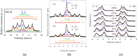
Figure 4. Mössbauer spectroscopy highlighting magnetic aspects of the semiconductor ZnO. (a) shows the distinctive sextet which is observable at room temperature and could be mistaken for structured ferromagnetic behaviour. (b) shows further measurements on the sextet where it was shown that the observed magnetism was due to slowly relaxing paramagnetism; (c) reveals the production of precipitates due to the clustering of Fe atoms at higher concentrations. Reproduced from [24, 26 and 27]. Copyright, AIP Publishing LLC.
Download figure:
Standard image High-resolution imagePerturbed angular correlation
PAC experiments require probe atoms which decay by a γ–γ cascade via an isomeric nuclear state. By measuring the two γ-quanta (γ1, γ2) in coincidence, an anisotropic angular distribution of the γ2 radiation is observed, and has been a standard technique at ISOLDE since the mid-1970s [28]. The main principles behind PAC are covered by the review of Frauenfelder et al [29] and are also covered in other contributions to this volume. Consequently, they will not be dealt with in detail here, with the exception of those which are most relevant to the solid state programme at ISOLDE. In contrast to MS described above, PAC is insensitive to the Coulomb interaction between the nucleus and the overlapping s-electrons and is not sensitive to the Debye–Waller factor. However, it enjoys the considerable advantage that PAC measurements are possible at temperatures up to and beyond the melting point of materials under study, which offers considerable flexibility in the choice of experiments. PAC allows the measurement of the local EFG and the magnetic field that a probe nucleus experiences when embedded in matter, independent of its physical state, i.e., solids, liquid, amorphous materials and molecules can be studied with PAC.
As 57Co is to MS, so is 111In to PAC: commercially available and widely used around the world. At ISOLDE, the programme focuses on other isotopes which are uniquely produced at ISOLDE. The two main isomers in this regard are 111mCd and 199Hg. These short-lived isomers (42 min and 49 min, respectively) account for about 80% of the PAC programme across both SSP and biophysics. In addition, several other isotopes such as 115Cd, 117Cd, and 111Ag have been employed in the past number of years to investigate various phenomena in nitride semiconductors [30].
At ISOLDE there exist several species of PAC spectrometers. These comprise 'traditional' analogue γ–γ setups comprising 4- and 6-detectors, such as has been described in earlier work by Butz [31]. Such a setup uses 12 or 30 coincidence spectra, respectively, which are combined to build the R(t) anisotropy ration function, i.e., the observable containing all the information regarding the coupling of the nuclear moments with the hyperfine magnetic and EFG. More recently, a concerted programme has been undertaken to digitize these analogue setups to take advantage of the increase in computational and electronic capability since the design of the original PAC setups in the early 1970s. Such setups are routinely used for experiments in both 4- and 6-detector configurations [32–34]. In addition, BaF2 detectors are now being replaced by LaBr3 and CeBr3, allowing for a considerable increase in the energy resolution, with good time resolution, and the number of isotopes which can be exploited for PAC.
Uniquely at ISOLDE there is also the possibility of employing β–γ and ec–γ PAC. A conversion electron—emitted in competition with the gamma ray of a certain transition of the decay cascade—can be used and correlated with another gamma ray or conversion electron from a different cascade transition. This opens up the possibility of employing eC–γ, γ–eC, eC1–eC2 PAC transitions to complement normal γ–γ PAC by extending the number of available probe nuclei, such as 73As/Ge, 77Br/Se, 80mBr/Br, 197 mHg Hg−1, 119mSn/Sn, 127Ba/Cs). Conversion electron PAC was extensively used at the University of Bonn using the Kleinheinz–Siegbahn spectrometer [35] which was later upgraded and installed at ISOLDE [36]. The eC–γ PAC spectrometer consists of an array of two magnetic lenses of the Siegbahn type for detection of conversion electrons [37] and two BaF2, scintillators for gamma detection, arranged in a plane as a standard 4-detector γ−γ PAC machine: a schematic and photo of the current setup is shown in figure 5. The samples are placed inside a vacuum chamber at the centre of the detectors, with the implanted side facing both magnetic lenses [36]. In the present setup samples can be measured as a function of temperature from 30 K up to 900 K. Once mounted on-line at ISOLDE, the tube placed between L1 and L2 (shown in figure 5) allows the implantation of short-lived isotopes into the sample. Conversion electrons emitted from the radioactive probes are focused into plastic scintillators, which are coupled to light guides and photomultipliers. At the centre of the magnets are lead cylinders shielding the scintillators from undesired gamma radiation. The corresponding coincident gamma rays are detected by BaF2 scintillation detectors opposed to the magnetic lenses as detailed in [36].
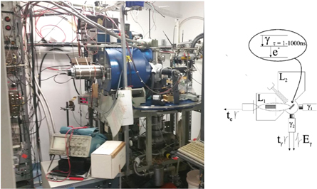
Figure 5. (left) Photo of the ec–γ PAC spectrometer and (right) a schema of the setup. L1, L2 represent the magnetic lenses placed 90° to each other, τ is the half-life of the intermediate state; te—electron timing signal (anode PM), the electron energy is defined by the magnetic field on the lens; tγ—gamma timing signal (anode PM); Eγ—gamma energy signal (dynode PM).
Download figure:
Standard image High-resolution imageExamples of probe nuclei, where only conversion electron PAC can work, are the cases of 73As/Ge (80.3 d) and 119mSn/Sn (293 d). The 73As/Ge electron capture nuclear transmutation provides a unique case of a semiconductor PAC probe. Via its 100% decay to a first 66.7 keV long-lived (0.5 s) state on 73Ge, allowing the full recuperation of the electronic shells. The decay is followed first by a 53 keV M2 gamma ray, then a fully converted E2 transition of 13.3 keV. In this case, it is necessary to use γ–eC coincidences to measure the PAC perturbation function. The 2.86 μs half-life of the intermediate 13.3 keV state provides high resolution identifying very low EFGs or magnetic fields [38]. The isomeric 119mSn/Sn decay requires the use of eC–γ coincidence PAC experiments due to the very high conversion coefficient of the first 65 keV M4 transition. This permits the study of hyperfine interactions which combine PAC with Mössbauer experiments on the same sample, which may be particularly interesting for temperature dependence measurements as the quality of the PAC signal is unaffected by temperature.
A unique feature of eC–γ PAC experiments, which is impossible with γ–e and γ–γ PAC cascades, is the ability to induce excited electron holes at the probe's atomic shells, prior to the beginning of a measurement. This allows one to follow subsequent electronic recombination. The observation window will be limited by experimental reasons to the time resolution of the experiment, typically of 1 ns. The observation of transient fields, depends not only on the host electron mobility and carrier concentration but also on the relationship of the probe-impurity-host, especially from the existence of long-lived local electronic excited states which can be probed in this way. For nuclei where both e–γ PAC and γ–γ PAC can be performed, such as 111 mCd/Cd−1, 199 mHg/Hg, 80mBr/Br, 181Hf/Ta, 127Cs/Ba, 100Rh/100Ru) these studies provide unique and unequivocal identification of carrier mobilities and lifetimes of electronic excited states at the probe atom [39].
An example of the information that can be derived from PAC experiments concerns phase transitions in multiferroic materials, where the coupling of charge and magnetism give rise to many phenomenological aspects. Pr1−xCaxMnO3 has an orthorhombic distorted perovskite structure and belongs to the class of multiferroic oxides, i.e., it shows a combination of ferroelectric and magnetic behaviour, which in this case is associated with the occurrence of Mn3+/Mn4+ valence charge order in the material. The PAC probe 111m Cd (48.5 min) was implanted into different Pr1−xCaxMnO3 compounds, where it is incorporated on Ca sites [40]. The EFG experienced by the probe atoms was then measured as a function of temperature figures 6(d)–(f) across the charge order (CO) phase transition that was established from the magnetic susceptibility figures 6(a)–(c). At low temperatures, in the CO regime, where the samples are ferroelectric or antiferroelectric, a slight temperature dependence of the main component Vzz of the EFG is observed, which decreases slowly with the increasing temperature until a prominent discontinuity is reached and a sharp increasing jump in Vzz occurs at a temperature TEDO—electric dipole ordering temperature—close to, but clearly below the charge order temperature TCO, followed again by a less sharp decrease. The soft temperature dependence of the EFG below TEDO was attributed to the onset of electrical dipole fluctuations at the probe site and TEDO itself is, hence, interpreted as the temperature where electrical dipole order is lost completely, which surprisingly occurs clearly below the temperature TCO where Mn3+/Mn4+ valence charge order itself is disappearing. In conclusion, the PAC measurements gave clear evidence for a new phase transition occurring below the charge order transition in Pr1−xCaxMnO3 and it was interpreted in terms of a paraelectric to (anti)ferroelectric first-order phase transition related to electric dipole ordering [41].

Figure 6. The application of PAC to multiferroic materials. The top part of the spectra show the temperature dependence of the inverse magnetic susceptibility for Pr1−xCaxMnO3 samples with x = 0.35 (a), x = 0.40 (b), and x = 0.85 (c). The bottom row shows the temperature dependence of the electrical field gradient Vzz seen by the radioactive 111mCd nucleus and corresponding fits below the charge order transition using the Landau theory of phase transitions for x = 0.35 (a), x = 0.40 (b), and x = 0.85 (c). Reprinted figure with permission from [41]. Copyright (2008) by the American Physical Society.
Download figure:
Standard image High-resolution imageRadiotracer techniques
Radiotracer techniques are the most flexible of the applied methods which are employed at ISOLDE. Here, the main focus is on utilizing the half-life or measuring characteristic gamma rays of the isotope which has been implanted. As such, the choice of isotopes is not constrained by specific decay properties and a wide variety of isotopes can be utilized.
Radiotracer diffusion
As mentioned previously, radiotracer diffusion is the oldest application of radioactivity in the field of SSP. Understanding the diffusion of impurities within a material is of crucial importance for the technological application of a material such as a semiconductor where the influence of e.g. transition metals in Si can greatly affect device performance [42], especially with the ever-decreasing size of devices. In addition, the behaviour of how the host elements self-diffuse in the crystalline lattice is of considerable importance. Although there are various other methods for determination of diffusion coefficients in materials such as secondary ion mass spectroscopy [43], radiotracer techniques allow for a very direct measurement of the diffusion profile which is strongly indicative of the diffusion mechanism of the species of interest. For specific applications such as highly diluted systems, self-diffusion and, in particular, studies of amorphous materials, radioactive tracers are especially useful. The increase in sensitivity—due to the ease of detecting radioactive decay—also allows for a clearer interpretation of data than is the case for non-tracer methods.
The experimental method for radiotracer diffusion is quite straightforward and is illustrated in figure 7. The desired isotope is implanted into the material being investigated. The sample is then heat-treated to allow for the diffusion process to take place. The sample is then sectioned, typically using a mechanical polishing rig, or by sputtering, and a gamma spectrum is recorded. By repeating the final two steps a profile of activity through the sample is built up from which a diffusion profile can be readily constructed. The first diffusion studies at ISOLDE were performed by Mehrer in Si [44] and subsequent studies also focused on elemental Si in its amorphous form. Au was found to diffuse in an anomalous manner; the diffusion of interstitial Au in a–Si was significantly retarded by the presence of intrinsic defects, presumably immobile vacancy-type defects which were responsible for trapping the Au atoms [45].

Figure 7. Typical experimental procedure for radiotracer diffusion. Samples are implanted at ISOLDE, annealed to repair radiation damage—and allow diffusion to take place. Samples are then sectioned and the polished activity is measured. Repeated numerous times, this allows a diffusion profile to be produced.
Download figure:
Standard image High-resolution imageMore recently, the focus has been on the diffusion processes in compound semiconductors such as CdTe. The pioneering work of Wolf et al [46] established the crucial effect between charged dopant atoms and the internal electric field in a material. In this case, if an inhomogeneous distribution of charged defects is present, an internal electric field is generated acting on any charged particle present in the semiconductor. An internal electric field can also be generated exclusively by intrinsic defects if they act as donors and acceptors and are inhomogeneously distributed. This has been found to give rise to the so-called 'uphill' diffusion profile which is nicely illustrated in figure 8(a). Here the profiles are shown for a range of radiotracers such as 111Ag, 67Cu, 193Au, and 24Na measured in CdTe crystals after implantation and subsequent diffusion under external Cd vapour pressure [47]. CdTe crystals are initially Te-rich but upon diffusion under a Cd atmosphere the surface regions become Cd rich due to the in-diffusion of interstitial Cdi. Since intrinsic CdTe point defects such as Cdi and Cd vacancies, VCd, form shallow donor and acceptor levels in the band gap, upon diffusion under Cd atmosphere pn-junctions are established on both sides of the crystal. This is a consequence of the fact that n-type regions with Cd-excess develop near both surfaces while a p-type region with Te-excess remains in the centre of the samples. When in thermal equilibrium with the host crystal, the fast interstitial donor impurities will mirror the profile of the electric potential across the crystal, in the present cases, by increasing the concentration in the Te rich region.
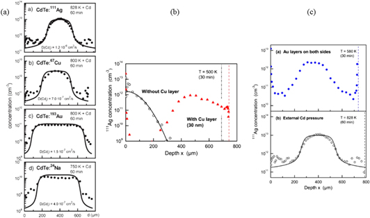
Figure 8. (a) Illustration of 'uphill' diffusion in CdTe following implantation of radioactive isotopes at ISOLDE (a); (b) shows the effect of metallic layers on the diffusion of 111Ag in CdTe; (c) shows the effect of Au layers on diffusion and also an over-pressure of Cd. [47] John Wiley & Sons. © 2010 WILEY-VCH Verlag GmbH & Co. KGaA, Weinheim. Reprinted with permission from [48]. Copyright (2012), AIP Publishing LLC.
Download figure:
Standard image High-resolution imageSubsequent studies have extended this anomalous diffusion behaviour to the role that metal contacts play with regard to the diffusion of impurities in semiconductors. The application of a thin metal Cu layer has the effect of producing the same uphill diffusion profile seen previously, and is due to the production of Cd self-interstitials at the metal/semiconductor interface [48]. This is very clearly illustrated in figure 8(b) where the control experiment before the application of the metal layer displays a monotously decreasing profile, while with the Cu layer the uphill profile is seen. In figure 8(c) the effect of twin Au metal layers is compared to annealing in a Cd rich atmosphere. The similar behaviour indicates that the uphill diffusion originates from the presence of Cd interstitials. The consequences of this work are considerable, the metal/semiconductor interface is an indispensable constituent for semiconductor devices. Understanding the influence of metal contacts for compound semiconductors will be required before these materials supplant elemental materials such as Si in the future.
The most recent developments in the diffusion programme have focused on the implementation of a new online chamber, which will allow for the study of the diffusion of short-lived isotopes in materials. This is shown in figure 9 and allows for implantation, annealing, sectioning and gamma measurement in situ. Rather than mechanical sectioning, this employs an Ar ion gun to remove the surface of the implanted material. This will greatly expand the possibilities of the diffusion programme at ISOLDE. Initial experiments with feldspar materials have been extremely promising where the properties of K diffusion have been measured [49]. In the coming years, a programme to understand the role of transition metals in technologically important materials such as CuInGaSe solar cells—one of the most efficient solar cell materials—will be followed where the unique possibilities offered at ISOLDE will be employed to understand the role of Cu diffusion in these materials, for which no current data yet exist.
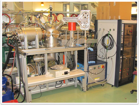
Figure 9. The newly commissioned online diffusion chamber which will allow diffusion studies of isotopes with half-lives in the minutes domain.
Download figure:
Standard image High-resolution imagePhotoluminescence (PL) spectroscopy
PL is one of the most widely used spectroscopies for the characterization of semiconductors. It has been the subject of several reviews and a detailed overview of its capabilities can be found in Lightowlers et al [50]. The principle behind PL is quite simple. Using laser light (which typically emits above the band gap of the material under study), a semiconductor is illuminated. This excites transitions within the material which recombine often at local impurities. This recombination is analyzed using a spectrometer and from this an optical spectrum characteristic of the material is produced. The main power of PL lies in the very high spectral resolution which is achievable and the rich detail which can be extracted from the spectra. A typical schematic of a setup is shown in figure 10. The laser energy produces a non-equilibrium concentration of free electrons and holes which begin to diffuse through the material. Electrons and holes may combine to form free excitons, some or all of which may be captured at donors or acceptors thereby producing bound excitons. Electrons and holes may combine directly with acceptors or donors, respectively, and a donor electron may recombine with an acceptor hole. Defects and impurities may occupy excited states by trapping electrons or holes. The recombination of electron–hole pairs and the relaxation back to their ground states of excited defects and impurities govern the nature of the PL spectrum produced. Most of these transitions are quite distinct and from the spectrum which is produced a detailed picture of the impurities present in the material can be drawn.
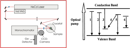
Figure 10. Schematic of a typical PL system: a laser is shone onto a sample held in a cryostat. Luminescence is collected by a spectrometer and analysed using a multichannel detector. In addition the various luminescence recombination processes are described on the right: 1—free exciton (FE or X); 2—bound exciton (BE, AX or DX); 3—electron to acceptor (e, A); 4—donor to acceptor (D, A or DAP); 5—hole to donor (h, D); 6—impurity or defect internal transitions.
Download figure:
Standard image High-resolution imageExcitons typically have quite low binding energies—of the order of 1–10 meV—although they can be higher in some wide band gap semiconductors. This requires that the best results in PL are obtained at sample temperatures <10 K and the bulk of the studies are carried out at liquid helium temperatures. PL is not intrinsically a quantative technique. Although the intensity of a spectrum does depend on the concentration of impurities present in a material, the various competing processes which produce the luminescence may be more efficient for some transitions than others with some transitions dominating the spectrum even while the concentration of the responsible defect centres may be considerably lower [51]. However, the main limitation on PL is its chemical blindness. Although certain instances exist for which stable isotope effects allow the identification of impurities, these are usually only observable for light impurities such as Li, see e.g. [52], the vast majority of spectra do not yield this information and chemical attribution needs to be inferred rather than measured, often through careful diffusion and/or implantation measurements.
The application of radioactivity to PL is a very clear way to remove this chemical blindness. The observation of either decay or growth related to introduced radioactivity allows for an unambiguous chemical identification of chemical species in the material. This was first realized in the mid-1960s with pioneering work by Broser et al [53] who measured Cu in ZnS. However, due to a lack of relevant radioactive isotopes the technique did not advance until the application of radiotracers for PL began to be pursued at ISOLDE. Initially confined to long-lived isotopes (>2 d), samples were prepared at ISOLDE and then shipped to home institutes where the PL measurements were pursued. This allowed for some notable results, including the identification of all Cd peaks in GaAs [54] but was limited due to the half-life constraints on which isotopes could be applied. The installation of a dedicated PL lab on-site at ISOLDE allowed these constraints to be overcome, and isotopes with half-lives of 1–2 h became standard probes for PL. In addition to broadening the range of isotopes which could be applied to this technique, shorter half-lives also means that a typical sequence of measurements can be carried out in 1–2 d (one usually measures the decay sequence over 5–6 half-lives), which puts less demands on keeping the system stable during this sequence. The laboratory at ISOLDE now consists of two multichannel detectors: an InGaAs array for infrared measurements and a CCD3000 for the visible and near UV range. A new analysing spectrometer was installed in 2016 and allows the full spectral range to be accessed without any experimental re-configuration. A closed-cycle two-stage He cryostat allows samples to be held at 4.5 K during the course of the measurement. Excitation is typically provided from the 325 nm laser line of a 80 mW HeCd laser. The most recent results have focused on the wide band gap semiconductor ZnO. The observation of room temperature lasing in ZnO [55] sparked considerable interest in the optoelectronic properties of this material. However, many of the fundamental properties of the material were unknown, including the chemical identity of many of the most prominent impurities which give rise to typical PL spectra. Radiotracer PL allowed the identification of many of the donor impurities which are present in ZnO. A full summary is shown in figure 11. Radiotracer work allowed for the identification of both singly and doubly ionised donors originating from Ga and In [56] after implantation of 72Zn. In addition, the first deep double donor—originating from Ge—was clearly identified following the decay of 73As [57]. Radiotracer PL also allowed the first observation of Sb being optically active in ZnO, apparently occupying a Zn site in contrast to predictions which indicate that this impurity should occupy an O-site [58].
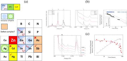
Figure 11. Overview of summary of the work on radiotracer PL carried out at ISOLDE. Donor impurities in both neutral and charged form have been successfully identified (a). (b) shows the clear identification of In as giving rise to both the I9 and I2 optical features; (c) shows the first observation of a optically active Sb in ZnO. Reprinted with permission from [58]. Copyright (2013), AIP Publishing LLC.
Download figure:
Standard image High-resolution imageRadiotracer PL was also applied to resolve some open questions in isotopically pure 28Si. This is an exciting material which is composed entirely of 28Si atoms. In contrast to standard Si, this material has allowed for a full re-evaluation on the nature of impurities and defects in Si due to the drastic reduction in spectral line width made possible due to the elimination of inhomogeneous isotope broadening. The inhomogeneous isotope broadening arises from the dependence of the Si band gap energy at low temperature on the average Si mass, coupled with the statistical fluctuations in the number of the three stable isotopes of Si within the effective volume of a given impurity or bound exciton state [59]. Of particular interest was the realization that many well-studied defect systems—especially those involving transition metals—were composed of complexes of 4–5 atoms rather than 1–2 as previously supposed. The decay to 197Au allowed the completion of this systematic study clearly identifying multi-atom complexes in line with previously studied systems involving Cu, Au and Li. In addition, the decay to 197Au and 197Pt allowed for more multi-atom centres to be identified. These results are summarized in numerous papers [60, 61] and have opened a considerable challenge to existing theory which remains open. Since this work, 28Si has found a unique application in the field of quantum computing and is one of the most promising materials for the realization of next generation devices. It currently holds the record for the longest coherence time in a solid state material [62].
Emission channelling
Emission channelling is a technique which is almost uniquely employed at ISOLDE, mostly due to the need to have large numbers of radioactive ion beams to investigate materials. At ISOLDE it is one of the most successful solid state methods and has been used to determine the lattice location of impurities in crystalline materials. It has been a mainstay of experiments at ISOLDE since 1985, evolving as detectors have improved to allow for more capabilities in terms of count rate and in the types of isotopes which can be studied using the technique. In emission channelling, the yield of charged particles, which are emitted from radioactive impurity atoms which have been implanted into the material, is measured for various high symmetry directions. This enables the location of impurity atoms within the crystal to a very high precision <1 Å. During decay, the nuclei emit charged particles i.e. α, β+/− and conversion electrons. As they travel through the crystal they experience either channelling or blocking effects. Along the principle crystalline axes, this yield is quite anisotropic and is dependent on the preferred lattice site of the impurity atom [63]. One of the clear advantages of emission channelling over other channelling techniques such as Rutherford backscattering is that any element—lighter or heavier than the host matrix—can be used without sensitivity loss, since only the existence of a radioactive isotope decaying with charged particles is required. Furthermore—in common with most techniques employing radioactive probes—the implantation doses are typically quite low <1013 cm−3, preventing amorphization of the lattice. A comprehensive early overview of work done at ISOLDE can be found detailing the role of Li in a variety of semiconductors [64] and also a summary of the work through the 1990s was given by Wahl [65].
The emission channeling collaboration at ISOLDE has been fortunate to profit from the synergies arising from being based at CERN In the late 1990s, a new form of position-sensitive detector was produced by CERN's silicon strip detector group [66]. Although originally envisaged to be of used for high energy physics and x-ray imaging, it was soon realized that these detectors should also be capable of detecting electrons, even though there was a compromise in performance due to the large entry windows and slow counting speeds. This was first tested in 1997 with the successful commissioning of a 3 × 3 cm2; 22 × 22 pixel detector [67].
The experimental demands for an emission channeling setup are relatively modest: a sample is mounted on a goniometer in a high vacuum chamber which is equipped with a heating device so as to perform annealing sequences. A great advantage of using the position-sensitive detectors mentioned above is that the angular accuracy restraints are reduced: as the sample is not moved during data recording, the angular accuracy of the goniometer is no longer crucial. This allows for less precise goniometers to be employed. Typical components of an emission channeling system are shown in figure 12.

Figure 12. Typical components of an emission channelling system. The most crucial being the position-sensitive detector and the goniometer.
Download figure:
Standard image High-resolution imageFor many years there was an inherent restriction on the choice of isotopes which could be employed in emission channeling experiments. For electron emitting isotopes—due to count rate level and noise related limitations of the detection systems themselves, it was impossible to use isotopes with half-lives below 6 h, as the count rate could not exceed 200 c/s [67, [68]. This was a frustration as there were many useful isotopes which could not be utilized as the short-lived decay would overload the detector.
At CERN a new generation of fast Si detectors has been developed which allows for up to 4000 c/s, and which can be used to measure isotopes with a more intense short-lived decay. This has allowed the development of a new online chamber which is capable of measuring isotopes with half-lives typically of the order of 1–2 h and in certain cases down to 10 s of seconds. This chamber is shown schematically in figure 13. This new online chamber has greatly expanded the possibilities of the emission channeling programme at ISOLDE and allows for the study impurities such as short-lived transition metals—potentially important for future spintronic materials—and also elements such as Mg, crucial in the doping of nitride semiconductors. Examples of some of the short-lived isotopes which have been used in recent times are: 11Be(t1/2 = 14 s); 27Mg (9.5 min), 56Mn (2.6 h) and 61Co (1.6 h). A full description of the new chamber can be found in a recent review article [69].

Figure 13. Schematic of the new online emission channelling setup at ISOLDE. Reprinted with permission from [69]. Copyright (2013), AIP Publishing LLC.
Download figure:
Standard image High-resolution imageIn practice, emission channeling measurements are typically recorded for 4 high symmetry directions and comparison is then made to theoretical calculations assuming certain lattice directions. The theoretical framework has been developed by Hofsaess and Lindner—the Manybeam program—[63] and was subsequently updated by Wahl [70]. This program calculates the angle-dependent emission channeling yields for any position in the lattice along any crystallographic direction. The starting-point is naturally the crystallographic structure of the host material. The three-dimensional structure is determined experimentally and from this the Manybeam formalism uses the two-dimensional projections with respect to the channeling axes. In addition, consideration is taken of the vibration amplitude of the crystal atoms, both of the host and the impurities. The output of the Manybeam calculations, for a given material, channeling axis and impurity isotope, is a two-dimensional emission pattern for each impurity lattice site and rms displacement. These patterns are smoothed using a Gaussian with σ ∼ 0.1° to account for the contribution of the 1 mm beam spot to the experimental angular resolution. In addition, the size and shape of the detector pads is accounted for by averaging the simulated yield which falls within an angular range of one pixel. This produces a two-dimensional pattern which is then used to simulate the experimental data.
Recent results from the emission channeling programme at ISOLDE have focused on the wide band semiconductors GaN and ZnO, in addition to group IV materials such as Si and Ge. The promise of ZnO as a host material for spintronics and its potential application in optoelectronics resulted in an immense effort to better understand this material, and especially with regard to the behaviour and nature of the main impurities [25]. In particular, the difficulty of producing p-type ZnO was studied with immense effort. The challenge of doping wide band gap materials is well known, with several self-compensation effects such as the creation of amphoteric impurities limiting the range of the Fermi level in thermal equilibrium [71]. At ISOLDE, emission channeling studied the case of As in ZnO, which—as a group V element—was suggested by numerous groups as a possible p-type dopant in ZnO by occupying the O-site [72]. Results from emission channeling gave the first clear evidence that As does not occupy the O site in ZnO, but due to the large mismatch in atomic radii (2.22 A for As3−; 1.38 A for O2−) the implanted As atoms occupied Zn sites rather than O. Upon annealing, it was found that the As continued to occupy Zn sites with a fraction located at a possible interstitial position. Although a small percentage could occupy the O-site, it was found to be insufficient for any useful p-type doping [73].
Recent experiments utilizing short-lived 27Mg beams have allowed for more precise studies of this crucial impurity in nitride materials. Although GaN can be made p-type through the introduction of Mg, efficient p-type doping is only achieved after electrical activation procedures, required to overcome the influence of H in these materials [74]. Another nitride material—AlN—has an extremely wide band gap of 6.01 eV and correspondingly has proved to be considerably more difficult to dope p-type. The importance of being able to clearly identify the lattice locations of impurities in materials was demonstrated by recent results using the online chamber described above. In particular, although Mg has been proposed as a p-type dopant in AlN, there were considerable inconsistencies among the community regarding its location in the lattice. The proposed locations ranged from substitutional Mg on an Al site to a highly deformed Mg–N complex, resulting in quite a displacement from the Ga site, to a less deformed Mg–N complex [75, 76]. Emission channeling is unique in being able to resolve these questions about the location of impurities in such materials. Following implantation of 27Mg into AlN it was found that the majority of the Mg atoms substituted for Al but a considerable fraction (33%) were found to occupy interstitial positions in the lattice, see figure 14. Above 600 °C the interstitial position was converted to substitutional Al with an activation energy in the range 1.1–1.7 eV. In addition, the displacements from the ideal Al location were smaller than predicted by some theoretical models [77].

Figure 14. Emission channeling following implantation of 27Mg in AlN, allowing for a greater understanding of the role of Mg in these nitride materials. Reprinted with permission from [77]. Copyright (2013), AIP Publishing LLC. The patterns show a 2D representation of the relative emission anisotropy from the implanted crystal. Blue represents the highest yield and the patterns are normalized to the random direction, which has no channeling effects. On the left the pattern pairs show the comparison between the best simulation fit and the experimental measurement. On the right the patterns show the theoretical spectrums for Octahedral interstitial site and the Al substitutional site. A linear combination of these is used to build the best fit to the experiment.
Download figure:
Standard image High-resolution image
A final example illustrates the importance of this technique in the field of magnetic semiconductors. (Ga, Mn)As is the prototypical dilute magnetic semiconductor [78] and is widely studied for the insights which can be gained about the behaviour of magnetic impurities within this matrix. The location of Mn is crucial to the magnetic behaviour of this class of materials: the majority of Mn impurities substitute for Ga while a minority occupy interstitial sites. Mns provides the localized magnetic moment and an itinerant hole for mediating the magnetic coupling. Interstitial Mn on the other hand has two additional compensating effects: coupling magnetically to Mns and compensating Mns acceptors: it is the interstitial Mn which determines the hole concentration, the Fermi level and also the effective Mns concentration [79]. In spite of the crucial role that interstitial Mn plays in (Ga, Mn)As, many aspects of its behaviour were poorly understood. In particular, the precise interstitial location in the lattice was unknown, and several inconsistent reports existed in the literature. Using a 56Mn beam from ISOLDE, emission channeling was able to pinpoint the precise location of the interstitial in (Ga, Mn)As, finding it to be the tetrahedral with 4 nearest As neighbours. The other possible site in the lattice—tetrahedrally coordinated with 4 Ga neighbours—was not found to be present, clarifying the long-standing dispute on the nature of interstitial Mn [80].
Perspectives for SSP at ISOLDE
This review has only allowed for a flavour of the SSP programme at ISOLDE. In particular, recent years have seen a considerable expansion in the types of materials being studied using radioactivity at ISOLDE. Although semiconductors still constitute about 50% of the materials under investigation, the new generation of low dimensional materials are also very much to the fore. This presents an opportunity but also a challenge to the community. The discovery of graphene in 2004 [81] ignited the field of low dimensional materials and led to the discovery of numerous others such as MoS which also display remarkable properties [82]. No less remarkable has been the scientific activity around these materials, which has led to thousands of papers being produced per year.
The solid state programme at ISOLDE has managed to remain relevant. One of the attractions of combining radioactivity with SSP is the ability to answer questions which are otherwise difficult or impossible to resolve. In particular, local effects can be probed using hyperfine interactions—using probes in a dilute manner, i.e. without interfering with the host materials. A programme understanding the surface properties of Hg ad-atoms on graphene is underway. Furthermore, topological insulators are being studied using a variety of methods from PAC to emission channeling in an effort to characterize the local interactions which underlie the basis of the topological interaction [83]. In addition, next generation solar cells—based on CuInGaSe2—are being investigated using Cu radiotracers. The behaviour of transition metals in such materials has a drastic effect on the overall performance [84]; and radiotracer methods allow the cleanest means of understanding diffusion processes in such materials.
In parallel to this, developments in ab initio codes such as WIEN2k [85] have allowed for a greater understanding of the processes being measured, especially for techniques such as PAC where the interpretation of data can be quite challenging. In addition, the continued development of new beams with increased levels of purity allow for constant opportunities for new applications to areas beyond nuclear physics. In spite of the pace of materials science—which can far outstrip the planning times required for nuclear or particle physics—the programme of SSP has remained relevant and continues to address challenging topics using the unique diversity of radioactive ion beams available to users at ISOLDE.
Acknowledgments
It is a pleasure to acknowledge the support of all the technical teams at ISOLDE for their continued work over the years in delivering high quality beams to the user community in solid state physics.
We gratefully acknowledge many years of support given to the maintenance and upgrade of the solid state physics laboratories and provision of large scale equipment by the Federal Ministry of Education and Research (BMBF) through different grants, including 05K13TSA and 05K16PGA, from Fundação para a Ciência e a Tecnologia (FCT) project CERN-FIS-NUC-0004-2015 and Research Foundation Flanders (FWO) in collaboration with the University of Leuven (KU Leuven). ASF acknowledges the PhD grants support by FCT (SFRH/BD/84743/2012) and KU Leuven. ED-B and ARGC acknowledge FCT-PhD grants (SFRH/BD/95865/2013 and SFRH/BD/86386/2012.