
Abstract
Radiation susceptibility of electronic devices is commonly studied as a function of radiation energetics and device physics. Often overlooked is the presence or magnitude of the electrical field, which we hypothesize to play an influential role in low energy radiation. Accordingly, we present a comprehensive study of low-energy proton irradiation on gallium nitride high electron mobility transistors (HEMTs), turning the transistor ON or OFF during irradiation. Commercially available GaN HEMTs were exposed to 300 keV proton irradiation at fluences varying from 3.76 × 10¹² to 3.76 × 1014 cm2, and the electrical performance was evaluated in terms of forward saturation current, transconductance, and threshold voltage. The results demonstrate that the presence of an electrical field makes it more susceptible to proton irradiation. The decrease of 12.4% in forward saturation and 19% in transconductance at the lowest fluence in ON mode suggests that both carrier density and mobility are reduced after irradiation. Additionally, a positive shift in threshold voltage (0.32 V and 0.09 V in ON and OFF mode, respectively) indicates the generation of acceptor-like traps due to proton bombardment. high-resolution transmission electron microscopy and energy dispersive x-ray spectroscopy analysis reveal significant defects introduction and atom intermixing near AlGaN/GaN interfaces and within the GaN layer after the highest irradiation dose employed in this study. According to in-situ Raman spectroscopy, defects caused by irradiation can lead to a rise in self-heating and a considerable increase in (∼750 times) thermoelastic stress in the GaN layer during device operation. The findings indicate device engineering or electrical biasing protocol must be employed to compensate for radiation-induced defects formed during proton irradiation to improve device durability and reliability.
Export citation and abstract BibTeX RIS

Original content from this work may be used under the terms of the Creative Commons Attribution 4.0 license. Any further distribution of this work must maintain attribution to the author(s) and the title of the work, journal citation and DOI.
1. Introduction
To meet the demands of high-power, high-temperature, and high-frequency applications, there is a growing trend towards using AlGaN/GaN high electron mobility transistors (HEMTs), particularly in defense and military applications such as radar, countermeasures, high-altitude aircraft, sensors, onboard imaging systems for satellites, data communication and guided weaponry, and spacecraft [1]. These devices offer tremendous potential but are also vulnerable to radiation damage from various sources such as neutrons, protons, electrons, and heavier particles. Protons found in space present the greatest hazard to devices due to their abundance of energies between 10 MeV and 100 MeV (90% of all charged particles in this range). While electromagnetic radiation and electrons can be shielded against by the walls of a spacecraft, protons and heavier nuclei can penetrate thick shielding and electronics packaging. However, shielding reduces the energy of the most prevalent protons found in space before they reach underlying electronics. Hence, for our investigation into the effects of proton irradiation damage, we will focus on the lower end of the energy spectrum. Low-energy protons near low earth orbit can harm space-based instruments and impact their functionality. This includes x-ray telescopes like Chandra [2] and XMM-Newton [3], which are suffering from exposure to soft protons, leading to damage to CCD detectors and loss of exposure time. Soft protons with energies ranging from tens of keV up to a few MeV mostly populate the solar wind and magnetosphere of the Earth. Therefore, understanding the effects of proton radiation on GaN HEMTs is crucial for developing radiation-hardened electronics for use in high-radiation environments.
GaN HEMTs show exceptional radiation tolerance due to the high threshold energy required for atomic displacement in GaN [4] and the formation of a two-dimensional electron gas (2DEG) in a confined cross-section. They also show a high dynamic annealing rate, which minimizes the effects of irradiation-induced defects [5–7]. The performance of GaN HEMTs is limited by high power density, thermomechanical stress, and high channel temperature and radiation can further exacerbate their performance [4, 8]. Degradation due to radiation in GaN is typically inflicted by the excitations of the electron clouds more than displacement damage (DD) [9]. This raises a very important question: can the electrical field in a biased GaN device influence its susceptibility? Most studies of radiation effects on GaN HEMT performance only consider radiation effects on devices in the OFF state, neglecting operational stressors, such as those listed above. Therefore, it is necessary to examine the combined impact of environmental and operational stressors on GaN HEMTs.
Preliminary studies on the effects of radiation on GaN technology indicate that it is highly robust against radiation and requires significant exposure before any degradation [10]. Numerous studies have documented the impact of proton irradiation or implantation, with differing energies, on AlGaN/GaN HEMTs [11–16]. The literature contains studies of proton-induced degradation in GaN HEMTs as a function of energy [17, 18], fluence [11, 12, 19, 20], gate length [12], fabrication process [21], substrate (Si, SiC, Al2O3) [22], isolation methods [23], surface passivation [24], electrical stress [25], bias state [18, 26–28], etc. The energy level used in various studies ranges from 100 keV to 105 MeV, with a minimum fluence of 1 × 10⁹ ions cm−2 and a maximum fluence of 1 × 10¹⁶ ions cm−2. Typically, most studies favor an energy level between 1 MeV to 2 MeV because this range exhibits a higher non-ionizing energy loss (NIEL) compared to higher energy protons. This NIEL is strongly correlated with the amount of DD that occurs in devices. Several studies have investigated the impact of irradiation on the transport properties of GaN HEMTs at various bias conditions.
While some studies have suggested that the presence of an electric field does not affect incoming ion radiation [18], others have shown dissimilar behavior between ON and OFF conditions [27, 29–32]. To evaluate the influence of irradiation on HEMTs, ionizing sources such as x-rays and 60Co have been employed under various bias conditions. One study reported variations in electrical characteristics during gamma irradiation as a function of device structure and bias settings, such as high gate and drain voltage [32]. Another study demonstrated that GaN HEMTs exhibit less susceptibility to 10 keV x-ray irradiation in the ON-state, with the excellent recovery of functionality after 350 krad total ionizing dose (TID). The behavior of these HEMTs in the ON-state was found to be better than in the OFF-state due to the influence of both vertical and horizontal electric field components, which minimize the effects of radiation on the dynamics of trapped charges. The effects of proton and x-ray irradiation, as well as hot carrier stress, on AlGaN/GaN HEMTs in two different processes were also studied, and both TID and DD effects were observed [27]. The study found that the magnitude of the effects varied significantly with applied bias during exposure, and a single, worst-case bias condition cannot be defined for all varieties of AlGaN/GaN HEMTs. Chen et al investigated the combined effects of 1.8 MeV proton irradiation and hot carrier stress on GaN HEMTs [28]. Devices irradiated in the semi-ON condition with 1.8 MeV proton showed more significant threshold voltage shifts and transconductance degradation than those subjected to high field stress alone or under grounded or OFF bias conditions. Relatively low energy proton beams impact on GaN HEMT has been studied without considering presence of electrical field during irradiation [14]. The underlying physical mechanism that controls GaN HEMT reliability is still unclear due to the simultaneous interactions between high vertical electric fields, mechanical stress, temperature and impinging energetic ions inside the device structure. Moreover, degradation induced thermo-mechanical stress is often overlooked in post irradiated device analysis.
It is important to note that the majority of the OFF condition studies in the literature used grounded state. Grounding the pins of devices during radiation is helpful for several reasons. Firstly, it helps maintain stability by providing a reference voltage level, crucial during radiation exposure as it can induce fluctuating electrical charges in the device. Secondly, grounding offers protection by safely discharging any excess charge induced by radiation, preventing potential damage from charge buildup. Charge buildup can also affect the incoming proton ions and may cause non uniform irradiation dose in the devices. There needs to be more systematic research on low-energy ion irradiation that considers the operating state of devices (ON or OFF state) during irradiation, which can significantly influence their reliability and tolerance to incoming irradiation [29]. In our prior investigation [33], we employed high-energy Au4+ ions at 2.8 MeV to explore the ON and OFF states of the identical GaN HEMT structure utilized in this study. This study aims to fill the existing research gap of low energy and high fluence proton irradiation on GaN HEMTs with in-situ biasing. In this study, we employ 300 keV protons where peak DD occurs near the end of range of the ion and the range is largely within GaN buffer layer. Our findings offer a thorough insight into device degradation resulting from the synergistic impact of bias conditions and increased fluence levels. This intricate interplay culminates in the eventual failure of the device.
2. Method
A commercially available multi-finger HEMT manufactured by Wolfspeed (CGH6008D), as shown in figure 1(a), that operates up to 6 W power at 18 GHz frequency and 40 V bias was employed in this work. The layer structure (figure 1(b)) reported by the manufacturer consists of a ≈ 20 nm Al0.22Ga0.78N barrier, a ≈ 1 nm-thick AlN interlayer, 1.4 μm-thick GaN buffer, and 100 μm-thick 4H–SiC substrate. The gate length is Lg = 0.25 μm. Devices are fabricated by growing heterostructures on 100 mm diameter semi-insulating 4H silicon carbide substrates using metal-organic chemical vapor deposition in a high-volume reactor and conventional microfabrication processes. Ohmic contacts are formed directly on the top AlGaN layer using Ti/Al/Ni/Au, while Schottky metal gate electrodes are formed by recessing through a first SiN dielectric to the AlGaN and then depositing Ni/Pt/Au metallization. The gate electrode is laterally extended with gate metallization to reshape and redistribute the strong peak electric fields at the drain-side edge. A source-connected second field plate (FP2) is also fabricated after the second passivation layer to shape the electric field further [34].

Figure 1. (a) Schematic of bulk GaN HEMT die wire bonded to an AlN ceramic chip carrier (b) schematic (not to scale) of the cross-section of GaN HEMT.
Download figure:
Standard image High-resolution imageIn-situ irradiation experiments are performed in the Ion Beam Laboratory at Sandia National Laboratories. An NEC 3 MV Pelletron accelerator is used, which is capable of accelerating ions extracted from most gases, including protons (H+). A custom vacuum chamber with various cable feedthroughs (e.g. BNC, SMA) for electronic part irradiations at different bias conditions was employed in this work. In this study, two devices were subjected to irradiation using 300 keV proton at a flux of 1.8 × 10¹⁰ ions (cm2s)−1 with or without an internal electrical field (ON or OFF mode). Two GaN devices were wire bonded to separate ceramic chips, which were then connected to external Keithley 2400 SMUs. The SMUs supplied voltage during the ON mode and facilitated in-situ measurement after irradiation in either the ON or OFF mode operations. During the ON mode, the devices were operated at VDS = 2 V and VGS = −2 V (VGS = −3.2 V is the pinched off voltage) within the radiation chamber. ON mode biasing may seem very small considering the device's typical applications. There are a couple of reasons for choosing this condition. The absence of packaging in our device, coupled with irradiation conducted in a vacuum chamber for extended periods (up to 2 h) to achieve high fluence, introduces the possibility of the device's temperature surpassing normal operating conditions. This temperature elevation could impact the wire bonding contact to the device. The specific bias conditions, VGS = −2 V and VDS = 2 V, serve as sweet spot for inducing both thermal and electrical stress in the devices. In the OFF state, all device pins were intentionally grounded [6, 7, 11, 17, 21, 28, 35–37]. This configuration was chosen to establish a uniform reference potential and ensure consistency during irradiation. In-situ ion irradiation was performed on both ON and OFF mode devices at three different fluence levels, namely 3.76 × 10¹¹, 3.76 × 10¹², and 3.76 × 10¹³ ions cm−2. All irradiations were performed at a normal incidence, and all experiments were performed at room temperature.
According to SRIM, the 300 keV proton range is around 2.2 μm (figure 2(a)), and the vacancy/damage peak occurs within the GaN layer. Ion Distribution and Quick calculation of damage option which uses quick statistical estimates based on the Kinchin–Pease formalism and default displacement energy for each element is selected to calculate depth-dependent vacancies produced by incident ion and recoils. As expected, it is shown in figure 2(b) that the concentration of vacancies generated in the HEMT device stack increases with fluence.

Figure 2. (a) Range of 300 keV proton ion and stopping power of electronic and nuclear interactions predicted by SRIM. (b) Vacancy density generated as a function of proton fluence and depth within the device structure.
Download figure:
Standard image High-resolution imageMicro-Raman spectroscopy measurements were performed using a WITec 300a Raman spectrometer with an excitation wavelength of 532 nm, 2 s integration time, and 30 accumulations. An 1800 l mm−1 grating was used along with a 100 × (NA = 0.9) objective lens. The laser spot diameter was ∼700 nm. Electron transparent specimens were prepared through the in-situ lift-out method using the FEI Scios-2 DualBeam focused ion beam (FIB) system, varying the ion beam current from 21 nA to 72 pA to minimize FIB damage during final thinning. transmission electron microscopy (TEM) and energy dispersive x-ray spectroscopy (EDS) analysis were performed in a 300 kV Tecnai G2 F30 S-TWIN operated in scanning TEM high-angle annular dark field (STEM HAADF) with a resolution of 0.17 nm.
3. Results and discussion
At VGS = 0 V, figure 3(a) highlights the trend of IDS versus VDS where the degradation rate of ON mode devices is higher compared to OFF mode devices. Even at the lowest dose of 3.76 × 10¹² ions cm−2, the forward saturation current exhibits a decreasing trend. Specifically, for ON mode devices, IDS drops by 12.4% at the lowest dose and further declines to 19.2% at the second highest dose level. However, OFF mode devices exhibit more radiation hardness, initially experiencing a 5.5% decrease in IDS, followed by a 16.6% decline. At fluence 3.76 × 10¹⁴ ions cm−2, ON mode devices exhibit five orders of magnitude drop in IDS, whereas OFF mode devices show only three orders of magnitude. Point defects induced by proton irradiation can negatively impact the sheet carrier mobility by carrier trapping and scattering, and the trapping leads to a decrease in carrier density. In addition, the output current curve exhibits a reduced initial slope when the drain bias is low.

Figure 3. (a) In-situ I–V characteristics of GaN HEMT at VGS = 0 V for ON and OFF mode devices as a function of fluence. This is a normally ON device and current can flow between the drain and source with no potential applied to the gate. The inset shows I–V curve in log scale as the current is very low after 3.76 × 10¹² ions cm−2 fluence. (b) Forward current degradation at various gate voltages for OFF mode devices as a function of fluence.
Download figure:
Standard image High-resolution imageIf the channel electric field in AlGaN/GaN HEMT devices is below the critical electric field, the reduction in the initial slope of the output curve and the saturation current are indicative of a decrease in both the density and mobility of the 2DEG [38]. The higher level of degradation in the ON-state may be due to filed-assisted defect migration which reduces the effect of dynamic annealing.
Figure 3(b) shows decrease in IDS for OFF mode devices as a function of gate voltage. As illustrated in figures 4(a) and (b), the decline in peak transconductance suggests a reduction in mobility since the transconductance (Gm) is directly proportional to mobility. In the ON state, there was a decrease in Gm from 212 mS to 171 mS or around 19% at the initial fluence of 3.76 × 10¹² ions cm−2. However, in the OFF mode, Gm initially decreased by 5.66% and then further reduced by 23.6% at the subsequent fluence of 3.76 × 10¹³ ions cm−2. At the final fluence of 3.76 × 10¹⁴ ions cm−2, the channel mobility became effectively zero for both ON and OFF mode devices. The reasons for these degradations may be due to the combined effects of carrier trapping and mobility degradation, enhanced by some level of mixing between the compositions at the AlGaN/GaN interfaces or scattering of carriers caused by the vacancies formed near the channel [11, 13]. ON mode device cannot generate meaningful transfer curve after 3.76 × 10¹² ions cm−2 due to the damage induced by combined high field stress and irradiation at the same time. Due to the linear increase of critical voltage with gate length, the gate length of our device, which is relatively thicker, is more susceptible to degradation caused by tensile strain induced by electric fields [39].

Figure 4. (a) Transfer characteristics and transconductance (a) ON and (b) OFF mode devices at VDS = 1 V.
Download figure:
Standard image High-resolution imageThere is also a difference in threshold voltage between ON and OFF mode devices. There appears to be a 0.32 V positive shift in voltage when in ON mode, compared to only a 0.09 V increase in OFF mode, when both modes are exposed to the same 3.76 × 10¹² ions cm−2 fluence. Positive shift indicates the creation of acceptor-like traps, such as Ga vacancies, by proton bombardment, which is widely reported [14, 40]. As the irradiation dose increases, more DD is generated around the AlGaN/GaN interface. This leads to a reduction in carrier concentration and mobility [41], and a greater positive shift of 0.39 V is observed at the fluence of 3.76 × 10¹⁴ ions cm−2 during OFF state. To calculate sheet carrier density (ns) and sheet carrier mobility (μ), we use two equations derived from charge control model [42]:
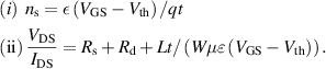
In this equation,  represents the dielectric constant of AlGaN, VGS represents the gate source voltage, where −1 V is used for the calculation, Vth represents the threshold voltage derived from IDS vs. VGS curve, q represents the electronic charge, t represents the thickness of the AlGaN barrier layer, RS and RD represent the source and drain access resistances, respectively, and W and L represent the gate width and the length, respectively. The ns and μ of pristine devices are measured to be 1.36 × 1013 cm−2 and 1823 cm2 (V·s)−1, respectively. After exposing the devices to a fluence of 3.76 × 10¹² ions cm−2, the ON mode device experiences a 10.4% reduction, and the OFF-mode device experiences a 19.4% reduction in μ. Both devices experience a 7% and 2% reduction in ns, respectively. OFF mode device further degrades by 52% and 8.5% in μ and ns respectively after 3.76 × 10¹³ ions cm−2 dose. The device in OFF-mode ceases to function after being exposed to the highest dose of 3.76 × 10¹⁴ ions cm−2.
Figures 5(a) and (b) show forward and reverse gate I–V characteristics of GaN HEMTs as a function of bias conditions and fluence. The decrease in forward current and increase in leakage current suggests that the control of the gate over the channel has weakened with an increase in fluence, specifically in ON mode operation. We employed Cheung's approach [43] to measure the series resistance to discern the impact on ON versus OFF states (table 1). The increase in series resistance (Rs) in the GaN HEMT with rising irradiation dose indicates a reduction in the product of mobility and free carrier concentration. This decline in mobility results from the introduction of defect centers acting as scattering points for charge carriers. Concurrently, the presence of deep traps associated with point defect DD reduces the free carrier concentration. These deep traps capture free carriers in the crystal lattice, leading to a decreased carrier density. The escalating density of radiation-induced defect centers, directly proportional to fluence, intensifies carrier removal, ultimately contributing to the observed rise in Rs and a subsequent reduction in forward current in the GaN HEMT in ON mode devices. The gate forward current changes towards different directions after proton irradiation at ON and OFF states. This variation can be attributed to variations in the series resistance. Our analysis revealed a significantly higher series resistance value in the OFF state after proton irradiation. Another contributing factor may be the substantial shift in turn-on voltage for ON-state devices after irradiation. Typically, Schottky barrier diodes exhibit a lower forward voltage drop compared to conventional diodes. However, ON mode devices deviate from ideal Schottky diode characteristics, which is evident in a higher ideality factor and an almost zero turn-on voltage. Beyond a fluence of 3.76 × 10¹² ions cm−2, ON mode devices exhibit a zero turn-on voltage as if there is no barrier at the junction, which is not possible. This underscores the increased vulnerability of ON mode devices due to the simultaneous presence of an electric field and self-heating in the device. During ON mode operation, the creation of a leakage path between the gate and buffer layer [44], caused by the combined effect of irradiation and gate bias stress, results in a significant six-order magnitude increase in reverse current. The barrier height (φbn) reduced, and the ideality factor (n) increased during both ON and OFF mode operation which are calculated based on thermionic emission equation [45]. This suggests that both the thermal emission current and the tunneling current were enhanced. Proton irradiation has the potential to generate defects in the AlGaN layer, causing the trapping of positive charges. This phenomenon amplifies trap-assisted tunneling effects where carriers overcome potential barriers by tunneling through energy states associated with the introduced defects. This phenomenon ultimately results in a higher leakage current. Moreover, the scanning TEM (STEM) images presented in figures 7(b) and (c) reveal a greater dislocation density in ON-mode devices compared to OFF-mode devices. Elevated dislocation densities can contribute to increased leakage in GaN-based HEMTs [46]. The large decrease in the barrier height of the ON mode device is also an indicator of a large increase in leakage current compared to OFF state devices. In comparison to the ON state, the OFF mode device exhibits less degradation in leakage current due to a relatively less drastic change in barrier height and dislocation density (figure 7(c)). An interesting observation is noted at the highest fluence, where a decrease in leakage current occurs unexpectedly. This unexpected stability in IGS at lower fluence and improvement in gate leakage at higher fluence can be attributed to the reduction in gate area resulting from void formation. The void formation mechanism, facilitated by Ni/Au inter-diffusion through vacancy exchange (the Kirkendall effect), involves radiation-induced vacancies assisting Ni diffusion up to the Au layer in the GaN HEMT gate terminal [47]. Additionally, an increase in oxygen at the AlGaN surface after irradiation has been reported, creating a potential barrier for electrons, and reducing gate leakage current. It is worth noting that similar trends were not observed in ON mode devices, suggesting that the presence of an electric field may rearrange defect distribution, leading to different electrical behavior compared to the OFF state device.

Figure 5. Degradation of Schottky gate forward and reverse I–V characteristics as a function of operation mode, (a) ON and (b) OFF, and fluence.
Download figure:
Standard image High-resolution imageTable 1. Sheet carrier density and mobility, threshold voltage, ideality factor and SBH (Schottky barrier height) as function of proton fluence of Ni/Pt/Au Schottky contact in AlGaN/GaN HEMT. Gate area is 1.2 mm × 0.25 µm. The data is missing in certain radiation conditions since no meaningful transfer curve could be generated due to device degradation.
| Pristine | 3.76 × 10¹² ions cm−2 | 3.76 × 10¹³ ions cm−2 | 3.76 × 10¹⁴ ions cm−2 | ||||
|---|---|---|---|---|---|---|---|
| ON | OFF | ON | OFF | ON | OFF | ||
| Sheet carrier density, ns (cm−2) | 1.36  13
13
| 1.26  13
13
| 1.33  13
13
| — | 1.24  13
13
| — | — |
| Sheet carrier mobility, μ (cm2 (V s)−1) | 1823 | 1633 | 1476 | — | 874 | — | — |
| Threshold voltage (Vth) | −2.57 | −2.25 | −2.48 | — | −2.18 | — | — |
| Series Resistance, Rs (Ω) | 2.41 | 2.91 | 9.02 | 28.52 | 20.86 | 421.6 | 535.5 |
| Ideality factor (n) | 1.57 | 5.27 | 1.573 | 6.91 | 1.557 | 4.81 | 2.786 |
| Barrier height, φbn (eV) | 0.96 | 0.35 | 0.94 | 0.27 | 0.927 | 0.36 | 0.787 |
To probe the physical mechanisms driving device degradation, we conducted high-resolution TEM (HRTEM) analysis near the AlGaN/GaN interface for both ON and OFF mode devices. Based on SRIM (Stopping and Range of Ions in Matter) measurements, we determined that 300 kV protons do not fully penetrate the GaN HEMT device structure. Consequently, all H+ ions remain within the GaN layer, potentially acting as trap states. The energetic H+ ions displace Al, Ga, and N atoms, and the recoil energy from these displaced atoms results in a knock-on effect, causing intermixing around the AlGaN/GaN interface where the 2DEG layer is generated. SRIM simulations indicate that the Al, Ga, and N profiles in the AlGaN barrier layer are broadened by approximately 5 nm, which contributes to interfacial roughening and performance degradation of the irradiated HEMT [48]. Figures 6(a) and (b) demonstrate this radiation-induced atomic intermixing by comparing HRTEM images of pristine and OFF mode ion-irradiated samples, respectively. In the pristine condition, the AlGaN/GaN interface appears abrupt, as seen in figure 6(a), which is crucial for maintaining a piezoelectric field at the interface. The piezoelectric effect is necessary for achieving high electron mobility and sheet carrier density in HEMTs [43]. However, after 3.76 × 10¹⁴ ions cm−2 proton irradiation, both ON and OFF mode devices exhibit less abrupt AlGaN/GaN interfaces due to interfacial roughening and intermixing, as seen in figure 6(b). The disorder observed at the crystalline interface indicates the presence of point defects that can scatter carriers or act as acceptors, such as Al vacancies, within the 2DEG layer, thereby degrading the electrical performance [11]. Geometrical phase analysis (GPA) was employed to map the strain at a nanoscale precision using HRTEM images of pristine and irradiated samples shown in figure 6(a). GPA maps are shown in figure 6(b). This method identifies parts of the lattice that exhibit deviations from the equilibrium lattice compared to the regular lattice in the AlGaN or GaN layers. We observed atomic defects in both pristine and irradiated interfaces. However, after irradiation, the AlGaN–GaN interface experiences strain relaxation and exhibits a higher defect concentration. After irradiation, the GaN layers experience significant dislocation, indicated by the presence of blue and red pairs in the GPA map.

Figure 6. High-resolution TEM image of the GaN/AlGaN interface of (a) pristine and (b) ion irradiated of 3.76  1014 ions cm−2 fluence of OFF mode devices. The interface is less abrupt after irradiation. The geometrical phase analysis (GPA) analysis of GaN HEMT's HRTEM (high resolution transmission electron microscopy) of pristine and ion irradiated with AlGaN/GaN interfaces are shown to the right side of HRTEM images. The intensity color bar represents strain value in percent (the value range of the scale bar is different for each image).
Download figure:
Standard image High-resolution imageLow magnification HAADF (High-angle annular dark-field) imaging reveals formation of dislocation in GaN layer after irradiation in both ON and OFF state devices as shown in figures 7(b) and (c). Interestingly, a higher concentration of dislocations is observed in the region between the gate and drain terminals, indicating a localized effect of the irradiation due to larger electrical field stress between these regions. Furthermore, the ON state device exhibits a noticeably higher concentration of dislocations compared to the OFF-state device. Metal from the drain contact has also diffused into the GaN layer as depicted in figure 7(c) by a yellow box. This indicates significant temperature rise during ON condition combined with proton irradiation of 3.76 × 10¹⁴ ions cm−2. High energy particle strikes create point defects that can agglomerate into extended defects like dislocation loops in materials. When a proton ion traverses through a material, it can also induce ionization by displacing electrons from their positions within the target material. As a result, electrons absorb a fraction of the energy and transition to higher energy states. Subsequently, when these electrons eventually return to lower energy states, the excess energy is emitted often as thermal energy, transferring to neighboring molecules. This process leads to the generation of thermal energy within the surrounding materials. Thermal stress during ON state further promotes dislocation formation and similar defect structure concentrations to increase in GaN layer and degrades device performance.

Figure 7. HAADF images of (a) pristine (b) OFF and (c) ON state devices. ON and OFF devices are irradiated with a fluence of 3.76 × 10¹⁴ ions cm−2. The dislocation appears as white lines in the GaN layer. The yellow box shows the diffusion of drain terminal metal into GaN layer.
Download figure:
Standard image High-resolution imageFigures 8(a) and (b) display the EDS box scan, conducted perpendicular to the AlGaN/GaN interface, revealing radiation-induced atomic intermixing and disorder. In figure 8(a), we observed broadening of the Al profile (∼3 nm) extending into the GaN layer after irradiation. This broadening of Al is expected to be accompanied by a similar broadening of Ga and N. However, due to the proximity of the AlGaN layer to the GaN layer, we were unable to resolve the broadening of Ga and N individually. Nevertheless, it is anticipated that this broadening would contribute to interfacial roughening and the degradation of electrical characteristics in the irradiated HEMT [48]. The impact of H ions on the device leads to atoms experiencing significant recoil energies, causing them to be dislodged from their original lattice sites. This initiates a chain reaction of further collisions, resulting in additional atomic intermixing. The 'Detailed Calculation with full Damage Cascades' model option in SR also predicted the broadening of elements in the AlGaN layer and the infiltration of Si3N4's N atoms into the AlGaN layer. Both phenomena have the potential to significantly alter the properties of AlGaN, leading to a decrease in transport properties.

Figure 8. (a) EDS box scan through a cross-section of the HEMT before and after the highest dose of H+ radiation in this study. (b) HAADF image of the GaN/AlGaN interface after the highest fluence of H+ radiation. The yellow box is where the box scan is performed to get the Al profile. (c) An overlay EDS image near the interface.
Download figure:
Standard image High-resolution imageRaman scattering spectra are collected at room temperature for comparison between the pristine and H ion-irradiated samples from the region indicated in figure 9(a). The Raman spectra collected from pristine devices operating in both ON and OFF modes exhibited no notable differences. During the experiment, the z(-, -)z ¯ back scattering geometry was utilized to observe the E2 (High) and A1 (LO) modes of GaN. There is no significant shift observed in the peak positions (not shown here). However, the only observable change is an increase in the full width at half maximum (FWHM) of the A1(LO) mode from 6.7 cm−1 to 7.1 cm−1 after exposure to a dose of 3.76 × 10¹⁴ ions cm−2. The FWHM broadening of the A1(LO) mode suggests reduced crystal quality and a decrease in phonon lifetime due to scattering by defects created from proton irradiation at room temperature.

Figure 9. (a) Optical images of the commercial AlGaN/GaN HEMTs wire bonded device with the inset showing a closer look of the measurement location in the channel. The bright dot above the channel indicates the position of the laser spot used for measurement. (b) Typical Raman spectra of the pristine sample indicating E2 (high) and A1 (LO) peaks. The inset shows the output drain current and drain voltage characteristics at pinched off state (Vg = −4 V) and ON state (Vg = −1 V) used during Raman measurement. (c) and (d) Comparison of operating temperature (ΔT) and bi-axial thermoelastic stress (σ) at two different device's dissipated power levels measured in the channel region of pristine and 3.76 × 10¹² ions cm−2 irradiated devices.
Download figure:
Standard image High-resolution image
In-situ micro-Raman spectroscopy, with the sample biased during measurement, was utilized to determine operating temperature (ΔT) and bi-axial thermoelastic stress (σ) simultaneously, using the peak shifts of E2 (high) and A1 (LO) phonon modes. Figure 9(a) shows a wire bonded sample under the Raman microscope and the inset shows the measurement location which is on the drain side close to the gate terminal. GaN devices inherently exhibit significant intrinsic or residual strain resulting from lattice mismatch and layer contraction during cooling from deposition to room temperature, even in unbiased conditions. In addition to the residual strain, high-voltage operation generates thermoelastic stress as electrons, accelerated under a strong electric field, transfer energy into phonons, which have slower energy transport. This energy localization near the gate region leads to significant joule heating and stress induction due to the thermal expansion coefficient (CTE) mismatch. Radiation damage further exacerbates this situation by altering stress distribution and thermal transport phenomena [8, 49]. By treating the pinch-off state, VGS < Vth (threshold voltage), as a reference and considering the approximate equality of the vertical electric field in both the pinched off state and ON state, the electric field parameter can be decoupled. Thus, utilizing the E2 (high) and A1 (LO) modes alone is sufficient to measure ΔT and σ as two unknowns. Extracting the parameters from peak shifts are obtained from the following matrix (details of this method can be found in [50, 51])
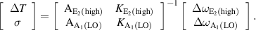
The temperature coefficient A and biaxial stress coefficient K used in the analysis were obtained from literature sources [50–52] where they were measured and compared using various methods such as XRD, Raman, photoluminescence (PL), and ab initio (DFT). The reported values exhibit an agreement within 10% accuracy or better. In the experimental setup, the pinched off state is defined as Vg = −4 V, while the ON state corresponds to Vg = −1 V for pristine sample and −0.5 V for 3.76 × 10¹² ions cm−2 irradiated sample to match dissipated power. In the Raman spectra displayed in figure 9(b), we can observe the peaks of interest. The inset of the figure showcases two operating conditions that aid in determining unknown parameters.
The findings indicate that the irradiated sample experiences higher temperatures due to self-heating compared to the non-irradiated sample, and this effect is amplified with higher operating power as shown in figure 8(c). This temperature escalation can be attributed to the reduction in the thermal conductivity of the GaN layer, stemming from phonon scattering caused by defects induced by the irradiation process. The irradiated sample exhibits a significantly larger increase in σ (approximately 0.3 GPa compressive) at an operating power of 1.3 W, representing a remarkable 750-fold increase compared to the pristine condition, as seen in figure 8(d). These results provide compelling evidence of device degradation resulting from strain modification caused by ion irradiation. Moreover, the presence of high in-plane stress during device operation has the potential to alter the interaction between energetic ions and the material, exacerbating the deterioration of the devices' mechanical and thermal properties. Devices operating in the ON mode are more vulnerable to irradiation damage due to the substantial increase in temperature they experience. This elevated temperature, combined with the thermal stress resulting from the simultaneous exposure to irradiation and operational stresses, renders them more susceptible to damage.
The long-term reliability of post-irradiated electronics in GaN HEMTs poses a challenge due to limited understanding of the processes involved in defect nucleation and propagation under applied and inherent stress in these devices. To ensure the wide range of applications for GaN HEMTs, it is crucial to conduct a more comprehensive investigation that delves into the underlying physics of damage caused by radiation and various localized stressors. This investigation would encompass diverse operating conditions such as ON, semi-ON, and pinched off states, as well as considerations of temperature and electrically pre-stressed conditions. By gaining a deeper understanding of these factors, a more robust framework for ensuring device reliability can be established.
4. Conclusion
In summary, we have thoroughly examined the effects of 300 keV H+ radiation on AlGaN/GaN HEMTs. This investigation encompassed various radiation doses and considered two distinct operating conditions: ON and OFF states. Increasing proton fluence led to a significant degradation in device performance. For ON mode devices, IDS decreased by 12.4% at the lowest dose and further declined to 19.2% at the second highest dose level. OFF mode devices showed more radiation hardness, with an initial IDS decrease of 5.5%, followed by a 16.6% decline at the lowest dose. This IDS reduction was attributed to carrier trapping and scattering caused by proton irradiation. The degradation in mobility (μ) was proportional to the reduction in transconductance (Gm) for both ON and OFF modes. At the highest fluence, channel mobility reached zero, rendering the devices non-functional. After irradiation, the Schottky gate's I–V characteristics revealed a substantial increase in leakage current, with a six-order-of-magnitude rise in the ON state and a one-order-of-magnitude increase in the OFF state. Additionally, the barrier height (φbn) decreased significantly, by 62.5% in the ON mode and only 18% in the OFF mode. HRTEM analysis revealed atomic intermixing and strain relaxation at the AlGaN/GaN interface after irradiation, leading to a higher defect concentration in both ON and OFF mode devices. GPA demonstrated strain mapping at the nanoscale, showing significant dislocation in the GaN layer, particularly in the region between the gate and drain terminals. The localized effect of irradiation was attributed to increased electrical field stress in these regions. EDS analysis confirmed atomic intermixing and broadening of Al by ∼3 nm in the AlGaN layer after irradiation, contributing to interfacial roughening and device degradation. In-situ Raman scattering spectra revealed significant rise in self-heating, amounting to a 59% increase, and a remarkable increase of 750% in thermoelastic stress after lowest proton fluence irradiated devices indicating device vulnerability to operate at high power in harsh radiation environment. ON mode devices are more susceptible to irradiation damage due to significant temperature rise and associated thermal stress generated from combined irradiation and operational stresses.
Acknowledgments
The authors would like to thank Mr. George Burns (Sandia National Lab) for his assistance. This work was funded by the Defense Threat Reduction Agency (DTRA) as part of the Interaction of Ionizing Radiation with Matter University Research Alliance (IIRM-URA) under Contract Number HDTRA1-20-2-0002. Aman Haque also acknowledges support from the US National Science Foundation (ECCS # 2015795). The content of the information does not necessarily reflect the position or the policy of the federal government, and no official endorsement should be inferred. This work was performed, in part, at the Center for Integrated Nanotechnologies, an Office of Science User Facility operated for the U.S. Department of Energy (DOE) Office of Science. Sandia National Laboratories is a multi-mission laboratory managed and operated by National Technology & Engineering Solutions of Sandia, LLC, a wholly owned subsidiary of Honeywell International, Inc., for the U.S. DOE's National Nuclear Security Administration under Contract DE-NA-0003525. The views expressed in the article do not necessarily represent the views of the U.S. DOE or the United States Government.
Data availability statement
The data that support the findings of this study are available upon reasonable request from the authors.