

Abstract
Conductivity is a fundamental property of materials; in particular the precise quantification of electrical sheet resistance is essential for the development of electronic thin-film devices. Conventionally, resistive probes are used to perform the corresponding measurements. However, non-invasive methods are more desirable as they minimize the required sample preparation, as well as geometrical influences. Existing non-contact conductivity measurements mostly rely on the transmission of electromagnetic waves through conductive thin-films. Hence, they only characterize translucent samples at high frequencies. We present an alternative technique based on the attenuation of low frequency 10 kHz electric fields. The approach is used to quantify the field-effect induced conductivity variation of a flexible indium-gallium-zinc-oxide semiconductor film. A custom-built high-impedance electrometer is used to capacitively measure the attenuation of an alternating electric field passing through the film. The obtained data is discussed and related to the absolute conductivity with the aid of two bespoke models describing the impedance mismatch between the sample and its surroundings. The sheet conductivity is modulated and measured from 660 nS to 116 µS
 while conventional DC current/voltage measurements serve as a reference. Both methods show a high degree of correlation to the reference measurements. Unlike techniques based on light, the low frequency signal used here resembles quasi-static characteristics, and enables the direct measurement of DC parameters.
Export citation and abstract BibTeX RIS
1. Introduction
Recent developments in thin-film technology and novel electronic materials including oxide-, 2D-, organic-, or nanowire-based semiconductors have enabled the realization of alternative electronic devices such as flexible, transparent, high-speed and large area systems [1–3]. Traditionally, the electrical properties of such semiconductor layers, most importantly their sheet resistance, is characterized using current/voltage measurements employing resistive contacts between the measurement apparatus and the sample under test. This is a well-established technique; nevertheless, there are certain issues which require further attention. First, sheet resistance measurements require exact knowledge of the lateral dimensions, and control of current spreading effects inside the layer under test. Hence, often measurements and approximations based on van-der-Pauw geometries with 4 contacts are used [4]. Second, resistive contacts are often not easily employable in combination with novel materials, as they can cause Schottky barriers, large contact resistances, or galvanic reactions, which can influence the measurement results significantly [5]. Additionally, the fabrication of resistive contacts small enough to probe certain samples, such as graphene flakes, is complex and can damage the surface of the sample under test [6, 7]. In this context, non-contact electrical characterization methods offer an alternative solution to prevent damage to the sample, without the need for significant sample preparation. Common non-contact techniques to quantify physical properties such as the specific resistance of conductive films include: scanning electron microscopy [8, 9], scanning tunneling microscopy [10], conductive atomic force microscopy [11], and electro-orientation spectroscopy [12]. Additionally, non-invasive conductance measurements based on the reflection and absorption of electromagnetic waves in thin conductors gained considerable attention [13, 14]. In 1956, Tinkham reported the first characterization technique based on infrared transmission [15] where it was described that the attenuation of light in conductive films is not related to the penetration depth (i.e. skin-depth) of the conductive film, but linked to the impedance mismatch between the sample and the surrounding. In equation (1) published by Tinkham, the power transmission ratio TP through a substrate with and without conductive coating is modeled by [15]:
where Y is the admittance of a conductive film under test, n is the refractive index of the substrate, and Z0 is the impedance of free space (i.e. the surrounding air). This value is 377 Ω [16]. The electrical properties of the conductive film can be determined if the substrate is transparent and its refractive index is known at the measurement wavelength. Recently, a similar method based on Terahertz radiation to measure the sheet resistance of Ag nanowire films on polymer substrates was developed [17]. Furthermore, microwaves can be used to measure the conductivity of graphene layers [18]. However, in addition to the sample thickness limitations, these methods are only capable of directly measuring high frequency performance parameters, and not low frequency and DC parameters necessary for the comprehensive characterization of conductive materials. To overcome these limitations, we present an alternative partially non-contact method to measure conductivity. The presented approach relies on monitoring the attenuation of electric (not electromagnetic) fields caused by a conductive thin-film. In contrast to electromagnetic radiation, this alternative method allows the use of lower frequencies to directly measure quasi DC parameters. This is particularly important for novel non-crystalline materials such as InGaZnO and organic semiconductors, where charge trapping and de-trapping occurs at frequencies in the mega Hertz regime [19]. Furthermore, the use of low frequency electric fields expands the range of possible substrates to any nonconductive material. The method relies on the direct measurement of electric potentials with micrometer spatial resolution using a virtually ideal non-contact electrometer in conjunction with a physical model to extract the specific sheet resistance of the characterized film. The presented method is verified by quantifying the conductance of an amorphous indium-gallium-zinc-oxide (IGZO) thin film [20] while the conductance is varied over multiple orders of magnitude by a field effect.
2. Experimental details
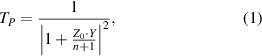
The measurement principle is illustrated in figure 1(a). A sinusoidal excitation voltage with amplitude of 1 Vp is applied to a metallic contact (labeled as field emitter) to generate an electric field. This electric field is then measured using a capacitively coupled high input impedance, electrometer. By placing a conductive thin-film between the emitter and the electrometer, it is possible to measure the attenuation of the electric potential caused by the thin-film. This attenuation varies with the sheet conductivity of the thin-film under test. To validate this technique, an additional DC bias voltage (VBias ) is also applied to the field emitter. The VBias modulates the carrier density and thus the resistance of the semiconductor field under test due to field effect. This bias voltage is affected by the sinusoidal excitation voltage, however this effect is averaged out over many cycles of the excitation signal. The excitation signal is applied by a GW-instek AFG-2225 arbitrary function generator outputting a constant, sinusoidal signal with a frequency of 10 kHz.

Figure 1. (a) Illustration of the described conductivity characterization technique based on the attenuation of a low frequency AC electric field through a (semi)conductive thin-film, and the contactless electric potential measurement using a high input impedance electrometer. (b) Structure and layer thicknesses of the sample showing the thin-film semiconductor under test, an insulated metal layer acting as bias contact and field emitter, as well as two reference resistive contacts to validate the described non-invasive measurements. The electrometer tip was raster scanned 50 µm above the sample surface. (c) Optical micrograph of the sample.
Download figure:
Standard image High-resolution imageThe core of the electrometer is a custom-built voltage buffer employing a positive feedback topology to achieve an input capacitance of  300 fF and input resistance of
  300 GΩ. This unusually high input impedance was experimentally confirmed by measuring the cut-off frequency of a high pass filter formed by a calibrated coupling capacitor and the input impedance of the electrometer. Utilizing a 1.2 pF coupling capacitor results in a lower cut of frequency of 0.4 Hz. This translates to an input resistance of 331.6 GΩ. Consequently, the electrometer can be considered as a nearly ideal voltmeter [21] where electric potentials with frequencies down to the millihertz regime can be measured non-invasively without disturbing the electric field under test. The input capacitance of the electrometer Cin
can also be quantified using the calibrated 1.2 pF coupling capacitor. As the DC gain of the sensor is known and the coupling capacitor forms a capacitive voltage divider with the input capacitance of the electrometer, any voltage gain loss can be attributed to the presence of Cin
. Using the capacitive voltage divider equation, the calculated input capacitance in this case is approximately 300 fF. The measured noise floor of the electrometer is 3.5 nV/
300 GΩ. This unusually high input impedance was experimentally confirmed by measuring the cut-off frequency of a high pass filter formed by a calibrated coupling capacitor and the input impedance of the electrometer. Utilizing a 1.2 pF coupling capacitor results in a lower cut of frequency of 0.4 Hz. This translates to an input resistance of 331.6 GΩ. Consequently, the electrometer can be considered as a nearly ideal voltmeter [21] where electric potentials with frequencies down to the millihertz regime can be measured non-invasively without disturbing the electric field under test. The input capacitance of the electrometer Cin
can also be quantified using the calibrated 1.2 pF coupling capacitor. As the DC gain of the sensor is known and the coupling capacitor forms a capacitive voltage divider with the input capacitance of the electrometer, any voltage gain loss can be attributed to the presence of Cin
. Using the capacitive voltage divider equation, the calculated input capacitance in this case is approximately 300 fF. The measured noise floor of the electrometer is 3.5 nV/ with a 1/f corner frequency of 10 Hz. More details on the measurement principle and the underlying system design can be found elsewhere [22]. This voltage buffer consists of a matched pair of N-type JFETs in cascode configuration to reduce the input capacitance and the input bias current. Additionally, positive feedback techniques are used to neutralise the stray input capacitances arising from the vicinity of the sensing probe to any ground path, and active guarding is deployed to screen the sensing probe from external noise sources. The output from the buffer is then amplified with a voltage gain of 20 V V−1 before it is filtered by two 4th order Butterworth band pass filters. The filtered signal can then be further amplified and is digitised using a NI USB6210 data acquisition device.
To map the local variation of electric potential, the electrometer is mounted on a three axis positioning system with 6 µm increment in all axes. The positioning system is a repurposed PCB milling machine modified to be a computer controlled xyz positioning system driven by open loop stepper motors. The sensing area of the electrometer is 5 µm in diameter. A similar system was previously used to quantify local DC voltage variations [23], and to acquire high fidelity maps of electric potentials [24]. The electrometer is raster scanned at a constant height of 50 µm above the conductive thin-film. To acquire a single data point, the probe was kept stationary for 5 ms and then moved by 6.2 µm at a constant speed of 6 mm s−1 to the next location. The 50 µm probe to sample separation results in a coupling capacitance of ≈4 aF between the electrometer's sensing probe and the sample. The small coupling capacitance along with the ultra-high input impedance of the electrometer ensures that no conduction current is drawn from the field and thus the sample under test is not influenced by the measurement. A change in distance between the sample and the electrometer probe would only influence the coupling capacitance between them. As the distance increases, this coupling gets weaker and hence the amplitude of the measured signal is reduced. However, the transmission ratio is not directly influenced by the absolute measured amplitude. Therefore, while it is important to keep the sample to probe separation constant, its absolute value is less relevant. It is worth noting that the increase in the sample to probe separation results in lower spatial resolution when imaging the local variation in sheet resistance. Measurement of bent substrates is possible as long as the geometry of the sample does not change. This can be achieved by dynamically adjusting the z-axis of the positioning system to keep the sample to probe separation constant or by compensating for the variation in distance mathematically when post processing the data.
All measurements were performed by investigating the sheet resistance of a semiconducting film, acting as a conducive sample with variable conductivity. The structure of the sample is shown in figure 1(b). To simplify the setup and to modulate the semiconductor conductivity, the emitter and the thin-film under test were integrated into one structure. The sample used here is made from a semiconductor layer, two resistive contacts to perform conventional measurements as reference, and an underlying insulated metal contact acting as the field emitter and bias contact. The field emitter is fabricated in close proximity to the semiconductor film under test. This allows for the alteration of the properties of the semiconductor film using the field effect by applying different DC bias voltages to the metal–insulator-semiconductor stack. The test sample was manufactured using standard thin-film technology in combination with UV lithography. The sample fabrication process started by cleaning the substrate (50 µm thick insulating polyimide) with IPA, acetone and a subsequent ozone plasma treatment. The use of polymer substrate here illustrates that flexible and partially opaque materials can also be characterized without being directly influenced by the presented technique (the use of e.g. glass or insulated Silicon wafers would be equally possible). The metallic field emitter/biasing contact was fabricated by the evaporation and structuring of 35 nm Cr. This layer was insulated by 25 nm of atomic layer deposited Al2O3. Next, a 15 nm thick semiconducting amorphous InGaZnO film was deposited. This layer was RF sputtered using a pure Ar atmosphere and a ceramic InGaZnO4 target. The semiconductor and the insulator layers were structured using wet etching. Finally, two resistive reference contacts were deposited on the semiconductor film using evaporated Ti (10 nm) and Au (60 nm). An optical micrograph of a fully processed sample is shown in figure 1(c).
3. Results
Initially, the electrical properties of the semiconductor film were obtained by means of conventional I/V measurement using a Wenworth probe station in conjunction with a Keysight B1500 semiconductor parameter analyzer. This measurement serves as a reference to cross-correlate the presented technique. The measurement configuration is shown in figure 2(a) and the results for various DC bias voltages are shown in figure 2(b). The DC bias voltage is varied from −2 V to 4 V. For this biasing voltage interval, the n-type semiconducting IGZO film shifts from depletion to enhancement mode. Hence, the specific conductance of the semiconductor film is altered by several orders of magnitude. The measurement shows the expected modulation of the specific semiconductor current from ≈1 µA m−1 to ≈15 mA m−1. Furthermore, a DC voltage sweep between the two top resistive contacts (figure 2(d)) shows a mostly linear behavior, and thus confirms the Ohmic nature of the resistive reference contacts. At the same time, an increase of the resistance (decrease of the slope) is visible for larger DC voltages; this indicates a saturation behavior in the semiconductor film. The interaction between the bottom emitter/bias contact and the semiconductor film under test is also investigated. The capacitance between the semiconductor and the bottom emitter contacts is measured while the top resistive contacts are at 0 V potential (shown in 2(c)). The capacitance increases from 0.2 to 2.7 mF m−2 as VBias
is increased. This occurs as the semiconductor becomes more conductive and forms a parallel plate capacitor with the bottom emitter contact while the sandwiched Al2O3 is acting as dielectric layer. Additionally, a decrease in capacitance is observed for higher measurement frequencies. This effect is caused by trap states which cannot be occupied and de-occupied at high frequencies [25] and emphasizes the need for characterizing such samples using low frequencies ( 100 kHz) to avoid charge trapping. Finally, the leakage current measurement shown in figure 2(e) confirms the high quality of the employed Al2O3 insulator layer. As shown, the measured current is virtually independent of the applied bias voltages and stays below 0.1 A m−2. This corresponds to an absolute current of
  4 nA. Both measurements confirm that the coupling between the bottom emitter/bias contact and the semiconductor film is purely capacitive, where the maximum mutual capacitance is 3.4 mF m−2. At the excitation frequency of 10 kHz, this corresponds to a coupling impedance of 4.7 mΩ m2.
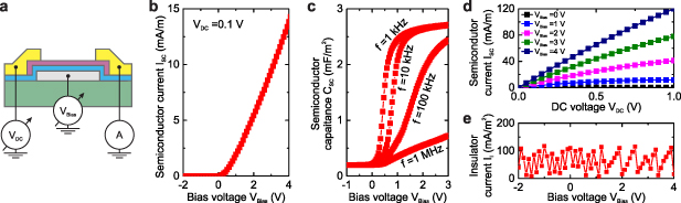
Figure 2. (a) Reference measurements for different bias voltages applied to the emitter/bias contact obtained using a conventional parameter analyzer. A DC potential difference of 0.1 V is applied between the top resistive contacts. (b) Resulting current–voltage characteristics. (c) Semiconductor capacitance measurements for various frequencies, acquired while both resistive contacts are grounded. (d) I/V characteristics measured while sweeping the DC voltage applied between the top resistive contacts. (e) Leakage current through the insulating Al2O3 layer for various VBias .
Download figure:
Standard image High-resolution imageThe measured maps of the local electric potential, attenuated by the semiconductor layer under test, obtained using the presented non-contact characterization technique are shown in figure 3(a). The amplitude of the AC excitation voltage applied to the emitter/bias contact is kept constant at 1 V and the amplitude of the top resistive contacts is set to 0 V. Similar to the reference measurements, VBias is incremented from −2 V to 4 V to vary the semiconductor conductivity via the field effect. Due to the capacitive nature of the measurement, the DC bias voltage is not sensed by the electrometer. Individual potential maps each containing 40 000 data points were recorded. The acquisition of each map took approximately 285 s. This is significantly longer than the virtually instantaneous conventional measurement of DC parameters. However, it has to be mentioned that the presented method also yields additional spatial information. Furthermore, for illustration purposes the scanned area was significantly larger than required. As shown in figure 3(a), the measured AC amplitude on top of the semiconductor film changes from nearly 1 V for VBias = −2 V (semiconductor acting as insulator), to 0.15 V at VBias = +4 V (semiconductor acting as a conductor). The resulting transmittance of the IGZO film versus various applied VBias voltages is plotted in figure 3(b). These values are obtained by averaging 540 individual data points acquired above the surface of the semiconductor film for each bias point as indicated in figure 3(a) (bottom right). The error bars represent the standard deviation.
Figure 3. (a) 2D images of local electrical potential variation acquired using the described non-contact technique. The measurements shows the reduction of electric potential caused by attenuation of the AC signal when passing through the semiconductor film. The amplitude of the AC excitation voltage is 1 V. The area used to extract the transmission data is shown in the bottom-right panel. A schematic drawing of the sample structure is added to improve clarity. (b) Quantitative data of the electric field transmission through the semiconductor film for different bias voltages, each value is obtained by averaging 540 individual measurement points. The error bars show the standard deviation.
Download figure:
Standard image High-resolution image4. Discussion
As described by Tinkham [15], the measured transmission can be linked to the film conductivity using the impedance mismatch model presented in equation (1). However, when using electric fields, the following assumptions are not fulfilled: (1) the Tinkham model was developed for EM waves and not electric fields; (2) the wavelength of the employed frequency is significantly larger than the lateral dimensions of the test structure; (3) the film under test is not metallic. Nonetheless, the Tinkham model can provide a valid approximation since the AC electric field and EM radiation behave similarly in the near-field, and the distance between the emitter/bias contact and the film under test is significantly smaller than the wavelength of the applied AC electric field. Consequently, the Tinkham equation can be adapted to accommodate the impedances present in the test structure to calculate the sheet resistance of the IGZO film:
Here, the absolute impedance of the semiconductor film (ZSC
) is given by  . For the applied excitation frequency of 10 kHz, ZSC
is 118 kΩ while the semiconductor film is conductive, and 1.65 MΩ when the film is depleted.
. For the applied excitation frequency of 10 kHz, ZSC
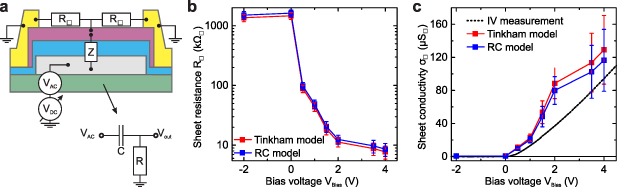
is 118 kΩ while the semiconductor film is conductive, and 1.65 MΩ when the film is depleted.  is the sheet resistance of the film, and n = 1.7 is the refractive index of the atomic layer deposited Al2O3 [26]. By using equation (2), the resulting sheet resistance for various bias voltages, extracted from the data shown in figure 3, is calculated and illustrated in figure 4(b). The graph shows the reduction of
  from 1.5 M
 to 8.6 k
 when the bias voltage is increased from −2 to 4 V.
Figure 4. (a) Illustration of the RC model used to calculate the sheet resistance of the semiconductor film based on the measured attenuation of the electric potential. (b) Sheet resistance of the semiconductor film for different bias voltages, calculated using the RC model and the modified Tinkham equation. (c) Comparison of the film conductivity extracted using both models with the values obtained from a conventional I/V measurement using Ohmic contacts.
Download figure:
Standard image High-resolution image
While the results obtained by the modified Tinkham equation are promising, the extraction of meaningful data without the need to make significant approximations is more desirable. Hence, an alternative lumped element model is also used to process the measured data (illustrated in figure 4(a)). The model relies on the impedance network formed by the capacitive coupling between the bottom electrode and the semiconductor film, as well as the resistance of the IGZO layer. This network provides a direct AC path to ground, which attenuates the electric field measured by the electrometer. This model considers the semiconductor to emit the measured electric field while being actuated by the capacitively coupled metallic emitter contact. The semiconductor layer and the emitter contact form a 1st order high pass filter. Thus the attenuation of the electric field can also be calculated using the network shown in the inset of figure 4(a). Similar to the adapted Tinkham model, the RC network model once again illustrates the premise that the observed signal attenuation is the direct result of impedance mismatch and not the absorption of the signal by the semiconductor film. The output voltage of the equivalent circuit formed by the capacitance of the semiconductor film CSC and the sheet resistance of the film is described by the following equation:
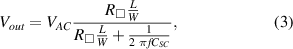
where VAC
is the applied AC excitation voltage. The absolute values of ZSC
is 1.3 × 10⁻¹⁰ F when the carrier density in the semiconductor film is high, and 9.6 × 10⁻¹² F when the film is depleted. The absolute resistance of the semiconductor is calculated using its sheet resistance  , its length L and its width W. The resulting
  calculated from this RC model is also plotted and compared to the results of the modified Tinkham model in figure 4(b). As shown,
  reduces from 1.3 M
 to 7.7 k
 when the bias voltage is increased from −2 to 4 V.
Finally, figure 4(c) compares the results obtained from the presented non-invasive characterization technique to the reference I/V measurements. Although the presented results cannot compete with the accuracy of resistive high-resolution measurements, both the RC and the modified Tinkham models are clearly correlated with the conventional I/V measurements. However, the measurement error of the presented non-contact technique can be tolerated if the added advantages such as the spatial map of electric potential are the relevant factor. It can also be concluded that the RC model is more accurate than the modified Tinkham model in this case. For negative bias voltages, the reference conductivity measurement is 50 times smaller than the conductivity extracted from the transmission measurements. This is due to the high levels of background noise associated with the electric field measurements, which was performed without any shielding in a electrically noisy environment. However, the obtained value for the turn on voltage of this semiconductor film from all three measurement techniques (i.e. 0 V) is in very good agreement. Compared to optical methods, the correlation between conventional and the presented non-contact conductivity measurements is slightly worse. Specifically, terahertz light measurements are able to determine the sheet resistance with  95% accuracy, but at the same time require complex calculations based on the Drude-Smith model to extrapolate the DC parameters from terahertz frequency measurements [17]. Furthermore, it is expected that placing the system in a fully shielded environment can further improve the signal quality by reducing the signal to noise ratio.
5. Conclusion
We have presented a non-contact technique to measure conductivity by measuring the attenuation level of an AC electric field transmitted through a conductive film. Two independent models based on the impedance mismatch between the conductive film and its surroundings were presented. Both models resulted in quantitative conductivity values for the investigated IGZO semiconductor film, which have high correlation to reference measurements obtained from the conventional I/V characterization measurements. The versatility of this approach was demonstrated by monitoring the modulation of the semiconductor film conductivity by multiple orders of magnitude using field effect transistor like structures. The presented method provides a new approach towards the unobtrusive and non-invasive characterization of novel electronic materials and functional thin films. If a suitable positioning system is used, the contactless nature of the present method can also have benefits for highly specialized applications such as the electrical characterization of devices in cryogenic environments by avoiding the creation of stress traditionally occurring at the interface between probe tips and sample with different thermal expansion coefficients [27].
Acknowledgment
This work was partially supported by EPSRC, GCRF, and NIHR, under the Contact No. EP/R013837/1 (SmartSensOtics).
Data availability statement
The data that support the findings of this study are available upon reasonable request from the authors.