

Abstract
The sputtering yield amplification (SYA) is a phenomenon based on doping a sputtering target with atoms of higher atomic mass. This doping changes the depth and the direction of the collision cascade in the target surface promoting a higher ejection of target atoms. In this work, we present a new way of generating the SYA phenomenon without the need of expensive and complex deposition systems. This was accomplished by increasing the working pressure and adding small pieces of W, as dopant element, on the racetrack of a Si target. The physical phenomena necessary to promote the SYA, for our experimental parameters, were analysed in two different deposition chambers and two sizes of sputtering targets. Based on the collisions in the gas phase, a calculation on the number of W atoms returning to the racetrack area was made, considering the number of atoms deposited on the thin films, to determine their effect on the cascade of collisions. In addition, calculations with the simulation of metal transport code were developed to determine the location on the racetrack zone the returning atoms were redeposited. By using reference samples placed on the racetrack of the Si target, we found that the percentage of SYA depends on the number of dopant atoms redeposited as well as the depth distribution these atoms had in the racetrack surface.
Export citation and abstract BibTeX RIS
1. Introduction
Direct Current magnetron sputtering is one of the most popular technique in the coatings industry due to its high deposition rate and versatility [1, 2]. However, despite its advantages the low deposition rate of some materials remains as a drawback [3, 4]. The sputtering process, as defined by Sigmund [5], is a multiple collision process that involves cascades of moving target atoms. These cascades may extend over a considerable region into the target although near its surface and can be separated into two stages. First, the slowing down of the primary ion and all the recoiling atoms that have comparable energies occur; those atoms will determine the spatial extent of the collisions cascade. Afterwards, the creation and slowing down of low-energy recoil atoms that will constitute the majority of atoms set in motion. Hence, the scattering events responsible for ejecting target atoms take place in a specific layer near the surface. Most of the ejected atoms comes from approximately 5 Å within the surface where low energy atoms are dominant.
However, adding heavy atoms at layers near the target surface, the sputtering process may change both the depth and the direction of the cascade of collisions. In 1992, Berg et al [6] investigated the sputtering yield amplification, SYA, by studying the Ar + C + Pt and the Ar + Si + Pt systems. He showed that the Pt atoms are implanted underneath the surface region of the C and Si targets. The collisions between the implanted Pt atoms and Ar ions, C and Si atoms result in the reflection of the lighter atoms. Thus, Pt atoms acted as effective reflection centres pushing the collision cascade to take place closer to the surface region, which helps to increase the number of collision cascades in it. The reflection effect will result in a substantial increase of the sputtering yield of lighter atoms. In the same study, Berg demonstrated that the SYA phenomenon is enhanced at low impurity concentrations. In order to explore the use of SYA, sophisticated and complex deposition systems as well as computer simulations have been developed to understand and apply this phenomenon [7–10].
The existence of C and Si SYA was reported using W atoms in a co-sputtering process [11]. In that work, W atoms redeposition on the target due to elastic collisions in the gas phase (at argon pressure of 4 Pa) was considered as the responsible process for SYA. Lieberman and Lichttenberg [12] suggested that for pressures  4 Pa there is no loss of secondary electrons, but does exist redeposition on the target and walls due to elastic collisions in the gas phase, according to the molecular mean free path equation 1. Whilst pressures
  4 Pa there is low scattering for the sputtered atoms from the target. Equation (1) shows that the mean free path, λ, is inversely proportional to the pressure, higher pressure implies greater dispersion of the sputtered atoms from the target within the deposition chamber
where, R, T, NA, and P are the universal gas constant, absolute temperature, Avogadro´s number and pressure correspondingly. The term  is related to the targets' cross-section of targets swept [12]
Although SYA has been studied extensively, it is not completely understood how the collision cascade is affected by the distribution of heavy atoms on the target surface and if the racetrack size becomes important. In this work, we will shed some light on the number of tungsten atoms needed on the target surface to produce the SYA effect. Also, an approximation of the volume within the target where the cascade of collisions should be redirected towards the surface is provided.
2. Experimental
Analyzed thin films were deposited with the same experimental procedure and parameters used elsewhere [11], where the SYA was studied for C, Ge, Al and Si targets by using W or Ti as dopant element. In the present work, the Si target experiments were revisited. Briefly, a 4'' diameter Si target (with a racetrack area of 23.1 cm2) was used and up to three W inserts were placed over the racetrack. The W inserts had 0.7 cm width, 2.5 cm length and 0.1 thick. The Ar gas flow was 20 sccm, to get a deposition pressure of 4 Pa. A constant supplied power of 20 W was used. The deposition time was 15 min with a target-substrate distance of 5 cm. In these experiments, small pieces from a Si wafer, as reference samples, were placed at two different positions on the racetrack: 90° and 180° with respect the location of the W inserts to analyze the returning W atoms to the racetrack. The surface elemental analysis of the Si pieces was determined by x-ray photoelectron spectroscopy (XPS) and Rutherford backscattering spectrometry (RBS).
Since the SYA does exist for experiments performed with a 4'' Si target, we repeated those experiments using a 2'' diameter Si target (99.99% of purity) in a different deposition chamber. For this target, the racetrack had an area of about 8.0 cm2. The W inserts (99.99% of purity) had sizes of 0.2 cm width, 2.0 cm length and 0.1 cm thick. They were placed one by one over the racetrack pasted with silver colloid ink. The deposition chamber was connected to a turbomolecular pump and two-stage mechanical pump to get a base pressure of 2 × 10⁻⁴ Pa. The deposition time was set to 30 min over glass substrates (2.5 cm wide by 7.5 cm long) which were ultrasonically cleaned with detergent solution, acetone and finally in iso-propanol prior deposition. Thin film deposition were performed at two different gas pressures: 0.9 and 4 Pa with a substrate-target distance of 4.5 cm. The pressure of 4 Pa was chosen because the mean free path of the sputtered target atoms was less than the target-substrate distance and subsequently there will be approximately three collisions between W atoms sputtered from the W inserts and the Ar atoms in the gas phase. Conversely, at 0.9 Pa the mean free path is larger than the target-substrate distance.
Thin films were studied via RBS by means of a 2.1 keV 4He beam from the Pelletron Accelerator at the Instituto de Física, UNAM. The RBS energy spectra were measured using a surface barrier detector set at 168° with respect the normal incidence. The alpha particle beam impinged perpendicularly at six different positions 1 cm apart on the substrate's long axis. The atomic concentrations for each spectrum was obtained using the SIMNRA code in order to know the number of Si and W atoms deposited in every position. Furthermore, the co-sputtering simulation (Co-SS) code [13] was used to calculate the spatial distribution of sputtered material with and without W inserts. In this way, we can determine the resulting sputtering yield as a function of the number of W inserts on the racetrack. The Si sputtering yield value was determined by normalizing the number of Si atoms deposited on the substrate, found by RBS, with the curve simulated via Co-SS as referred in [11]. Furthermore, computer simulations with the simulation of metal transport code, SIMTRA [14] are included to know the location where the W atoms are redeposited on the racetrack and to determine the energy they reached the racetrack surface
During the thin film deposition, the plasma spectrum was monitored in real time via optical emission spectroscopy (OES), through a suitable fused-silica viewport, from the vicinity of the sputter target (10 mm above the racetrack). The emission from the plasma was focused via a bi-convex lens (f = 15 cm) onto an optical fiber coupled to a compact CCD spectrometer (Avantes, AvaSpec2048CL, Dual Spectrograph). Two different detectors were used to obtain a 200–900 nm spectral range. Spectra were taken at a constant acquisition rate of about one spectrum every 1.2 s with an exposure time of 300 ms. In addition to the 0.9 and 4 Pa film depositions, intermediate pressures between these two limits, were only studied via OES to investigate the threshold pressure where Si SYA should occur.
3. Results
3.1. The 4'' Si target experiments
As the present work is based on an already published study on Si SYA [11], we will briefly discuss it prior presenting results from this work. Table 1, shows a summary of those previously reported results. The Co-SS code used 0.63 as Si sputtering yield, as reported in [15] for the experimental discharge voltage. After placing the W inserts, the Si sputtering yield was adjusted to match the resulting thickness (SYCo-Sputt); because the change on the discharge voltage did not fully explained the observed increment of the thin film thickness. The SYA is reported as a percentage increment with respect the pure Si target. The W sputtering yield was also determined to be 0.70.
Table 1. Silicon sputtering yield (SYSi) when only the change in the discharge voltage is taken into consideration. The Si sputtering yield (SYCo-Sputt) as a function of the number of W inserts as determined by the Co-SS code. The sputtering yield amplification (SYA) is also shown. (Adapted from [11]).
| Co-sputtering condition | SYSi (Vapplied) | SYCo-Sputt | SYA (%) |
|---|---|---|---|
| Si | 0.63 (740) | — | — |
| Si + 1 W | 0.63 (752) | 0.73 | 15.9 |
| Si + 2 W | 0.64 (758) | 0.91 | 42.2 |
| Si + 3 W | 0.63 (732) | 1.10 | 74.6 |
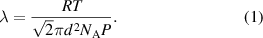
Once the target atoms are ejected in the sputtering process, they will have elastic collisions in the gas phase with the atoms from the working gas; the number of these collisions depends on the pressure. Besides, due to these collisions there will be deposition of those atoms over the walls of the deposition chamber. However, a significant amount of the total flux of ejected material will be redeposit on the target itself. To measure the W at.% deposited on the target, silicon reference samples were placed at the centre of the target racetrack at 90° and 180° with respect the location of the W inserts, see figure 1(a) inset. These samples were subject to a bombardment of 2 keV Ar ions to perform a XPS depth profile analysis, which is shown in figure 1(a). This graph shows this analysis for thin films deposited at a pressure of 4 Pa with 1 (blank squares), 2 (blank circles) and 3 (blank triangles) W inserts.
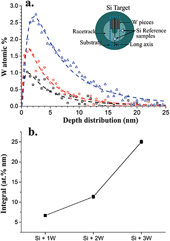
Figure 1. Si reference samples XPS depth profiles and their LogNormal distribution fits. Panel (a) shows how the W at.% increased as the number of W inserts. The inset indicates the location of the Si reference samples relative to the W inserts and the substrate. Panel (b) shows area under the LogNormal distribution fitted to the experimental data to estimate the amount of W atoms deposited on the Si racetrack surface.
Download figure:
Standard image High-resolution imageAccording to the XPS depth profiles, during the sputtering process W atoms were both redeposited and somehow buried on the target racetrack surface from the above plasma. However, due to their relative low impinging energy (see below) is very unlikely these atoms penetrate deeper than to about few nanometres (see figure 2). Hence, W atoms found at deeper locations may appear because of a knock-on process via collisions with Ar ions produced while sputtering. These ions are accelerated towards the cathode due to the applied voltage and may elastically collide with the redeposited W atoms burying them. According to our deposition parameters, these ions possibly reached the target surface at an energy of up to about 700 eV as shown in table 1. Besides during XPS measurements, the obtained depth profiles could be changed as a result of the 2 keV Ar ions impingement, especially the distribution tail.

Figure 2. SRIM simulations of the penetration of W atoms on a Si layer as a function of its energy. A deeper penetration on the Si layer requires more energy from the normal incident W atom.
Download figure:
Standard image High-resolution imageThe depth distribution of the W at.%, follows a Lognormal distribution (dashed lines in figure 1) with R2 values of 0.97, 0.99 and 0.98 for 1, 2 and 3 W inserts correspondingly; similar to an ion implantation profile as published by Ashworth et al [16]. With these experimental results there is no way to distinguish which part of the distribution is produced by either of the mechanisms described above. These graphs show that the W at.% increases as a function of the number W inserts. After they have reached their maximum value the distribution of W atoms begins to asymptotically descend with the depth. Nevertheless, using one or two W inserts result in an alike location of the maximum W at.% (about 1.2 nm); while for the three W inserts experiment this maximum is shifted to a depth of about 2.2 nm. This could be related to the total amount of W atoms redeposited over the Si target, which is estimated by the area under the distribution curve and is plotted in figure 1(b). The amount of redeposited W atoms did not increase linearly with the W inserts, but follows the same behaviour with the number of W atoms redeposited on the Si reference samples measured by RBS (see table 2). Moreover, the distribution of redeposited W atoms throughout the racetrack was approximately constant; according to the RBS measurements, the difference of the material deposited between the Si reference samples at 90° and 180° was lower than 2%.
Table 2. Atoms deposited at the substrate, at the target and as determined by the Calculation model for the 4'' diameter Si target and a deposition pressure of 4 Pa. RBS: Rutherford Backscattering measurement.
| 4'' target, P = 4 Pa, deposition time: 15 min (W atoms) | |||
|---|---|---|---|
| Co-Sputtering condition | RBS substrate | RBS Si reference samples [11] | Calculation (this work) |
| Si + 1 W | 2.1 × 10¹⁴ | 3.5 × 10¹⁴ | 3.4 × 10¹⁴ |
| Si + 2 W | 5.5 × 10¹⁴ | 5.0 × 10¹⁴ | 8.8 × 10¹⁴ |
| Si + 3 W | 1.0 × 10¹⁵ | 8.5 × 10¹⁴ | 1.6 × 10¹⁵ |
Figure 2 shows a SRIM [17] simulation of the depth W atoms can reach in a Si target as a function of its energy, at normal incidence. The graph gives an idea of the necessary energy that W atoms need to penetrate in the surface of a Si target. As can be seen, the depth distribution plotted in figure 1 is a combination of several mechanisms and becomes important to explain the observed Si SYA in the following sections.
3.1.1. A simple calculation of the number of W atoms returning to the 4'' target surface based on elastic collisions into the gas phase.
The number of W atoms arriving to the substrate from the 4'' diameter target was determined by means of the SIMNRA code using as input data the RBS experimental conditions. These results show that 2.1 × 10¹⁴ atoms cm−2s, 5.5 × 10¹⁴ atoms cm−2s and 1.0 × 10¹⁵ atoms cm−2 s were deposited on the substrate for one, two and three W inserts (see table 2). Sputtered atoms, which are ejected in a specific angular distribution [13], will suffer few collisions with Ar atoms at the gas phase on its way towards the substrate. Thus, the total sputtered flux can follow a linear combination of six possible directions (± x, ± y, ± z) after every collision. Bearing this in mind, the substrate and the target are in opposite positions and the z-axis is the distance between them. In this way, atoms that follow the trajectories (0, 0, 1) and (0, 0, −1) make their way to the substrate or returning to the target, respectively.
At a system pressure of 4 Pa the W atoms will have approximately three elastic collisions in their first 5 cm (the target-substrate distance) of its trajectory. For example, for one W insert, we can multiply the number of deposited atoms on the substrate, 2.1 × 10¹⁴ atoms cm−2s times 63 to estimate the total flux sputtered from the W insert. The resulting number is 4.6 × 10¹⁶ W atoms s−1 at the gas phase. With the total flux, we can calculate the returning W atoms on the target. Roughly, 1/6 of the sputtered atoms will continue the path towards the substrate (0, 0, 1) and, conversely, 1/6 of the atoms might arrive to the target (0, 0, −1) after their first collision. Atoms scattered in other directions, different from (0, 0 ± 1), can arrive to the target after their first collision as well, but their contribution to the calculation is negligible, because they would need another collision to make it. Consequently, for the experiment with one W insert, 8.0 × 10¹⁵ W atoms s−1 may return to the target via elastic collisions and might be able to be deposited throughout the racetrack. Then there should be about 3.4 × 10¹⁴ W atoms cm−2 s redeposited homogeneously on the racetrack surface area (23.1 cm2).
Repeating this procedure for two and three W inserts, the redeposited W atoms were 8.8 × 10¹⁴ atoms cm−2s and 1.6 × 10¹⁵ atoms cm−2s, correspondingly. These returning atoms towards the target correspond to roughly 17% of the total W sputtered flux. Those numbers are within the same order of magnitude of the RBS analysis made on the Si reference samples added to the racetrack, being these 3.5 × 10¹⁴ atoms cm−2s, 5.0 × 10¹⁴ atoms cm−2s and 8.5 × 10¹⁴ atoms cm−2 s, for one, two and three W inserts, correspondingly. With these conditions the Si SYA achieved for one, two and three W inserts were 15%, 42% and 74%. These results are summarized in table 2.
3.2. The 2'' Si target experiments
Figures 3 and 4 show the Si and W thickness distribution on the long-axis substrates due to the sputtered atoms from the Si target and the W inserts at two different pressures: 4 Pa (figure 3) and 0.9 Pa (figure 4). Figure 3 indicate the Si SYA calculated via Co-SS code (solid lines), from the RBS measurements which estimated an increment in the ejection of Si atoms (filled symbols), for one, two and three W inserts. Comparing the Si thin film grown without W inserts, the obtained amplification was 103%, 124% and 114% for 1, 2 and 3 W inserts correspondingly. For comparison, figure 3 also includes a simulation developed with the SIMTRA code using as input parameters the size and shape of the deposition chamber and substrate, 4 Pa, and considering 3 × 10⁶ particles. This curve, as the Co-SS simulations, was normalized to the Si RBS data.
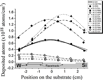
Figure 3. Silicon and Tungsten atoms deposited over the substrate long axis as a function of the W inserts (1, 2 or 3) estimated by RBS for a 2'' Si target and at a pressure of 4 Pa. The Si sputtering yield is determined via Co-SS simulations (Sim). A SIMTRA simulation curve is added to ilustrate the agreement with the Si Co-SS curve.
Download figure:
Standard image High-resolution image
Figure 4. Silicon and Tungsten atoms deposited over the substrate long axis as a function of the W inserts (1, 2 or 3) estimated by RBS for a 2'' Si target and at a pressure of 0.9 Pa. The Si sputtering yield is determined via Co-SS simulations (Sim). The circular geometry of the racetrack allows placing the W inserts in any zone without affecting the measurements.
Download figure:
Standard image High-resolution imageThe shift in the maximum of Si atoms in figure 3 corresponds to the larger ejection of the Si side of the racetrack for one and two inserts, this shift will be discussed in section 4.2. For three inserts two phenomena occurred: Si atoms have a symmetric deposition with respect to the centre of the substrate; and there is a decrement of the SYA with respect to the two W inserts experiment. These can be explained because of a saturation of W atoms on the Si racetrack surface, which affected the Si atoms ejection as well as its distribution on the substrate. The saturation effect reported elsewhere [8, 9] is due to the in- excess amount of doping atoms on the target surface, it usually appears when the concentration of the doping material is between 2.5 and 5.0 at.% of the target, depending on the studied material. After saturation occurs there still is SYA, however, it begins to decrease. These in-excess dopant atoms are rapidly ejected and, therefore, cannot affect the collision cascade, so they become part of the total ejected flux.This effect can also be observed in the OES results (see section 3.2.1). On the other hand, the low system pressure, at 0.9 Pa, (see figure 4) produced a much modest amplification, 10%, 10% and 13%, for one, two and three W inserts, correspondingly, indicating that the pressure is an important parameter to have W atoms redeposited on the racetrack and, consequently, to observe SYA. Those results are summarized in table 3.
Table 3. Silicon sputtering yield (SYSi) for the 2'' target experiment when only the change in the discharge voltage is taken into consideration. The Si sputtering yield (SYCo-Sputt) as a function of the number of W inserts as determined by the Co-SS code. Comparing these, the SYA was determined.
| System pressure (Pa) | Co-sputtering condition | SYSi (Vapplied) | SYCo-Sputt | SYA (%) |
|---|---|---|---|---|
| 4.0 | Si | 0.39 (402) | — | — |
| Si + 1 W | 0.37 (378) | 0.75 | 103 | |
| Si + 2 W | 0.38 (390) | 0.85 | 124 | |
| Si + 3 W | 0.35 (363) | 0.75 | 114 | |
| 0.9 | Si | 0.48 (517) | — | — |
| Si + 1 W | 0.47 (507) | 0.53 | 10 | |
| Si + 2 W | 0.47 (507) | 0.53 | 10 | |
| Si + 3 W | 0.47 (507) | 0.54 | 13 |
3.2.1. OES analysis for different system pressure.
To investigate the effect of the system pressure on the SYA phenomenon, the 2'' diameter target with up to three W inserts was sputtered at different pressures. Figure 5(a) shows the emission intensity of a Si I transition emitting at 251.61 nm while figure 5(b) shows a W I transition at 400.87 nm as function of the amount of W inserts. For all pressures, the emission from the Si I transition increased when one W insert was placed at the racetrack, however this emission increment was more noticeable at pressures above 2 Pa. At pressures below this value, the increment was only 32%; while at 2 Pa this increment was 84% and for 4 Pa the Si emission was sharply enhanced by 115%. With two W inserts the Si emission keeps increasing; however, while at low pressures the increment is approximately linear; at P ⩾ 2 Pa, appears to be nonlinear. Further increasing the number of W inserts to three pieces, no matter the system pressure, there is a negative effect on the emission enhancement of Si and it diminishes. This emission decay can be attributed to a W saturation effect mentioned above; then, the emission of Si atoms decreases and again, it becomes more important at high pressures. On the other hand, the emission of W (see figure 5(b)) remains approximately constant at pressures equal or below 2 Pa, where there are not significant differences between 0.9 and 1.3 Pa. The higher the pressure, the higher the emission enhancement comparing the emission of Si + 1 W and Si + 2 W. The two inserts condition seems to behave as a threshold condition for the saturation of W atoms at the target surface. Hence, there is not a significant W emission enhancement when another insert is placed on the racetrack. As a result, the observed W emission might be produced by not only sputtered atoms from the W inserts, but from redeposited W atoms as well, which were also sputtered. The variation of the discharge voltage (see figure 5(c)) with the pressure and amount of W pieces (a reduction of up to 10%) might not significantly change the plasma conditions, so the observed behaviour of both W and Si emission could be mostly explained by the number of sputtered atoms from the target only. Therefore, the Si and W emission can be correlated with the amount of Si atoms deposited on the substrate. While the Si emission increases 115%, 170% and 118% at 4 Pa; the maximum of the Si distribution on the substrate increased by 103%, 124% and 114% for 1 W, 2 W and 3 W conditions respectively.
Figure 5. Optical emission spectroscopy results for different system pressures as a function of the W inserts. (a) Emission intensity of the Si I transition emitting at 251.61 nm. (b) Emission intensity of the W I transition emitting at 400.87 nm and (c) discharge voltage.
Download figure:
Standard image High-resolution image4. Discussion
4.1. Effective volume of sputtering
The cascade of collisions at the target is affected by the addition of heavy atoms on the surface. Few heavy atoms produce the SYA phenomenon, an excessive number of them produce the saturation effect. However, the appearance of SYA suggests that a percentage of amplification depends on two mechanisms: the number of heavy atoms and the depth they reach into the target surface. It has been demonstrated that increasing the atomic mass of the dopant element not always change significantly the sputtering yield [9]. Sigmund [5] described three sputtering regimes, which depend on the Ar ion energy incidence: Knock-on, linear cascade and the spike regime. In the latter the number of recoil atoms is proportional to the energy deposited per unit volume and the cascade of collisions is thought to be nonlinear [18, 19]. Magnetron sputtering is usually within the linear cascade regime. However, by adding heavy atoms the number of sputtered atoms has a nonlinear behaviour. Then the sputtering yield will be a function on the percentage of the heavy atoms, how these are distributed over the target surface, and the energy of the impinging Ar ions.
For the 4'' Si target, Si reference samples were analysed by XPS to observe the redeposition of W atoms. The depth distribution of those atoms depended on the amount of the redeposited atoms, as shown by the Lognormal fittings in figure 1. There is a slight shift in the position of the maximum W at.% value with the number of W inserts, alike for one and two, close to 1.2 nm, and 2.2 nm for three inserts. Perhaps the sputtering process might promote this shift, although it is not clear the cause of it. Nevertheless, there was a larger area under the depth distribution of the W atoms with the number of inserts. During the sputtering process at the target surface, multiple collisions between the Si atoms with buried W atoms would exist, being this the cause of the SYA phenomenon. Thus, the length of the collisions cascade might increase, but this increment could be along the longitudinal direction (parallel) to the surface, and closer to the racetrack surface. The racetrack area along with the depth distribution generates an effective volume of sputtering. In this volume, the direction of the cascade of collisions is not only redirected towards the target surface due to collisions between Si-W atoms but also it is expanded longitudinally over the racetrack area; hence, more energy is being concentrated per unit volume, promoting a higher ejection of target atoms.
For one W insert on the racetrack, at 4 Pa, about 3.4 × 10¹⁴ W atoms were redeposited and buried with a specific and well defined Lognormal depth distribution. The maximum W at.% value was at 1.2 nm and then disappeared at a depth of about 17 nm, see figure 1(a). The cascade of collisions might be redirected towards the target surface from this depth distribution times the racetrack area (around 23.1 cm2). As a result, this effective volume of sputtering produced an enhancement of 15% in the Si sputtering yield. Moreover, increasing the number of W atoms and therefore their depth distribution into the racetrack surface the effective volume of sputtering increases improving the Si sputtering yield to 42% and 74%.
4.2. SIMTRA software simulations
Elastic collisions in the gas phase does exist, once the sputtered atoms leave the target, and the number of collisions depends on the working pressure. To further investigate, SIMTRA simulations were performed, so information on the redeposition location of W atoms over the racetrack surface as well as the energy can be obtained. These simulations were performed using as input data our experimental parameters: pressures from 0.9 to 4 Pa, size and shape of substrate and the deposition chambers, including the target-substrate distance, for the 2'' and the 4'' Si and W targets experiments, and considering 3.0 × 10⁶ sputtered atoms.
For sputtered Si and W atoms at 0.9 Pa, results show that energies of atoms bouncing back to the target were 2.2 and 2.7 eV respectively; while at 4 Pa these energies become 1.2 and 0.6 eV. The lower the pressure the higher the returning atoms energy. However, these results imply that both W and Si atoms reach the target at so low energy that they cannot sputter other Si atoms. On the contrary, they can only be redeposited on the target surface and unable to penetrate as inferred from results shown in figure 2. The simulation determined that for the experiment made at 4 Pa with the 4'' Si target about 15% of the total flux of sputtered W atoms would return to the target, whilst at 0.9 Pa would only return an almost negligible amount of 0.2%. However, even a little percentage of dopant atoms are able to change the cascade of collisions as shown in table 3.
Table 4 shows the fraction of the racetrack surface covered by the W inserts as well as the number of W atoms redeposited estimated with our simple calculation. Although the calculation of the redeposited atoms is very similar or in the same order of magnitude for both experiments, 2'' and 4'' Si targets at 4 Pa; the W atoms saturation effect was observed in the 2'' Si target only. This saturation could be due to the length of the mean free path, which is approximately 1.6 cm at 4 Pa, and the racetrack size. Figure 6 shows a comparison between the cross section of both racetracks; the 2'' target had a racetrack limited by two circles with radii 0.7 and 1.75 cm (figure 6(a)); whilst the 4'' target had a racetrack limited by the circles with radii of 0.7 and 2.8 cm (figure 6(b)). On the one hand, W atoms sputtered from the 2'' target racetrack would be able to return to the other side of the racetrack as a result of having one collision in the gas phase, only if it happens within the region where the 1.6 cm radii semicircles, drawn from the racetrack centre, intercept. This region is depicted by the striped area in figure 6(a). On the other hand, the 4'' target with their respective 1.6 cm semicircles have such an area far from the racetrack centre.
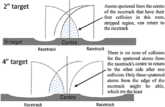
Figure 6. Schematic of the 2'' and 4'' target cross sections indicating the mean free path at a pressure of 4 Pa. The stripped zone where after one collision a sputtered atom is able to return to the racetrack's oposite side.
Download figure:
Standard image High-resolution imageTable 4. Relation between the W inserts and the racetrack area for both experiments, using the 2'' and 4'' Si targets. The redeposited W atoms as determined in section 3.1.1 is also shown.
| 4'' target (15 min) | 2'' target (30 min) | |||
|---|---|---|---|---|
| Co-sputtering condition | AW/ARt (%) | W atoms redeposited | AW/ ARt (%) | W atoms redeposited |
| Si + 1 W | 6.4 | 3.4 × 10¹⁴ | 2.5 | 2.4 × 10¹⁴ |
| Si + 2 W | 13.1 | 8.8 × 10¹⁴ | 5.2 | 4.2 × 10¹⁴ |
| Si + 3 W | 21.5 | 1.6 × 10¹⁵ | 7.8 | 6.3 × 10¹⁴ |
The shift in the maximum amount of deposited of Si atoms, towards the Si racetrack side (see figure 3) can be explained by the schematic model of semicircles. There is a SYA effect on the Si racetrack side, due to the few W atoms able to reach that region of the racetrack, which promotes a greater emission of Si atoms. Conversely, there is an extreme saturation effect of W atoms in the closest region where the W inserts were placed, which reduces the ejection of Si atoms.
SIMTRA simulation analysis of the redeposited atoms distribution confirms this idea. These simulations were performed with a grid of 2 mm by 2 mm squares to obtain enough spatial resolution of the redeposited atoms over the target relative to the 3.0 × 10⁶, which were used as input value in the simulations. Figure 7 shows the distribution of redeposited atoms on the target surface of 2'' and 4'' pure Si targets (a) and (b) and W targets (c) and (d). As may be expected, lighter atoms return at a higher proportion than the heavier ones; also, returning atoms are homogenously distributed in the angular direction. The radial direction shows a decrement of redeposited atoms as farther away from the target centre; however, within the racetrack region (area between dashed circumferences), the redeposition appears to be relatively homogenous. Moreover, figure 7(c) shows that the redeposition of W atoms on the racetrack area of the 2'' target, at 4 Pa, is higher than the 4'' target (figure 7(d)). This in-excess redeposition owing to the length of the mean free path, along with the racetrack size, may be the origin of the saturation observed with three W inserts over the 2'' target.
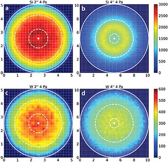
Figure 7. Redeposit of W and Si atoms on the racetrack area for 2'' and 4'' targets as obtained via SIMTRA simulations considering an input of 3.0 × 10⁶ particles. The colour scale indicates the number of atoms redeposited per grid point.
Download figure:
Standard image High-resolution imageFigure 8 shows the density of particles redeposited per unit area over the racetrack surface as a function of the system pressure, calculated from the simulations presented in figure 7. As it may be expected, a higher system pressure means more collisions in the gas phase, i.e. more atomic scattering in all direction inside the deposition chamber but mainly means a higher redeposition on the racetrack surface since the first collision occurs closer to it. This graph corroborates a higher density of W atoms on the 2'' target racetrack with respect the 4'' one, since these returning W atoms are redeposited in a reduced area.

Figure 8. SIMTRA simulation of the redeposited particles density on the 2'' and 4'' W racetracks as a function of the system pressure. The density is slightly higher for the 2'' target since the W atoms are redeposited on a reduced area.
Download figure:
Standard image High-resolution image
5. Conclusions
The SYA effect on Si targets with up to three W inserts placed on the racetrack for two deposition systems and two target diameters was studied. On the one hand, for a 4'' Si target the redeposition of W atoms on the racetrack surface was analysed via XPS. Results imply that the amount of W atoms affects the cascade of collisions in the sputtering process. Consequently, an effective volume of sputtering was generated which led to a linear amplification. On the other hand, results for a 2'' Si target suggested a saturation effect of W atoms on the racetrack surface with three W inserts. Moreover, the OES analysis corroborated the amplification itself as well as the saturation effect. These results are attributed to the mean free path, size and area of the racetrack. Our calculation, based on the collisions into the gas phase, gives a good approximation of the redeposited W atoms, which was corroborated by simulating the sputtering process via the SIMTRA code.
Acknowledgments
This work was supported by the National Council of Science, and Technology of Mexico, CONACyT (CB-2015-255156). Some of the equipment and laboratory facilities were provided by the National Laboratory of Nanofabrication (NANOFAB) and partially supported by PAPIIT-UNAM Grant Nos. IN112918 and IG101220. Julio Cruz acknowledges his postdoctoral fellowship from CONACyT.
Data availability statement
The data that support the findings of this study are available upon reasonable request from the authors.