

Abstract
Phase-change memory (PCM) is an emerging non-volatile memory technology that has recently been commercialized as storage-class memory in a computer system. PCM is also being explored for non-von Neumann computing such as in-memory computing and neuromorphic computing. Although the device physics related to the operation of PCM have been widely studied since its discovery in the 1960s, there are still several open questions relating to their electrical, thermal, and structural dynamics. In this article, we provide an overview of the current understanding of the main PCM device physics that underlie the read and write operations. We present both experimental characterization of the various properties investigated in nanoscale PCM devices as well as physics-based modeling efforts. Finally, we provide an outlook on some remaining open questions and possible future research directions.
Export citation and abstract BibTeX RIS

Original content from this work may be used under the terms of the Creative Commons Attribution 4.0 license. Any further distribution of this work must maintain attribution to the author(s) and the title of the work, journal citation and DOI.
1. Introduction
Phase-change memory (PCM) is a key enabling technology for non-volatile electrical data storage at the nanometer scale. A PCM device consists of a small active volume of phase-change material sandwiched between two electrodes. In PCM, data is stored by using the electrical resistance contrast between a high-conductive crystalline phase and a low-conductive amorphous phase of the phase-change material. The phase-change material can be switched from low to high conductive state, and vice-versa, through applying electrical current pulses. The stored data can be retrieved by measuring the electrical resistance of the PCM device. An appealing attribute of PCM is that the stored data is retained for a very long time (typically 10 years at room temperature), but is written in only a few nanoseconds. This property could enable PCM to be used for non-volatile storage such as Flash and hard-disk drives, while operating almost as fast as high-performance volatile memory such as DRAM.
Another particularly interesting emerging application for PCM is non-von Neumann computing. In this computing paradigm, the memory devices are not only used to store data but also to perform some computational tasks. By having a memory device that can compute, one eliminates the need of transferring data back and forth between the computing (CPU) and memory (DRAM) units that are physically separated in conventional computers. This physical separation and associated data transfers are arguably one of the main bottlenecks of traditional von Neumann digital computers, as a memory access typically consumes 100 to 1000 times more energy than a CPU operation [1].
As a pure memory technology, the potential of PCM has been demonstrated in a wide range of works in the past 10 years and the main remaining challenges are arguably related to cost, product-level fabrication and high-level integration in a computing system [2]. The successful launch of Intel Optane in 2018, a non-volatile memory based on PCM that can be used to enhance the existing memory-storage system, demonstrates the viability of PCM to be used as a digital memory in a standard computing system. Because of this, a detailed understanding of the underlying physical mechanisms and state dynamics of PCM is important for finding out how the technology can be further optimized. Such an understanding would also be helpful to find out how PCM properties can best be used for emerging non-von Neumann computing applications. Despite the fact that the memory effect in phase-change materials was discovered over 50 years ago, there are several open questions relating to electrical transport, the crystallization mechanism, relaxation effects, and inherent stochasticity in PCM, all of which are central to its operating principle.
In this article, we provide an overview of the current understanding of the PCM device physics that underlie the WRITE and READ operations. In section 2, we present a historical overview of PCM along with its basic operation principles and potential applications. In section 3, we cover the device physics related to the WRITE operation, including thermal characteristics, crystallization mechanism, threshold switching, and inherent WRITE stochasticity. In section 4, we cover the mechanisms that play a role in the READ operation, including the temperature and voltage dependence of electrical transport, resistance drift, and noise.
2. Essentials of phase-change memory
2.1. Historical overview
PCM exploits the behavior of so-called phase-change materials that can be switched reversibly between amorphous and crystalline phases of different electrical resistivity. The amorphous phase tends to have high electrical resistivity, while the crystalline phase exhibits a low resistivity, sometimes three or four orders of magnitude lower. This large resistance contrast is used to store information in PCM (the high-resistance state can represent a logical '0' while the low-resistance state can represent a logical '1'). Thus, a PCM device essentially consists of a layer of phase-change material sandwiched between two metal electrodes (see figure 1).

Figure 1. Operation principle of PCM. The mushroom-type PCM device displayed consists of a layer of phase-change material sandwitched between a top electrode (TE) and a narrower bottom electrode (BE). A long low current pulse (SET) is applied to bring the PCM device to the low-resistance crystalline state. A short high current pulse (RESET) is applied to bring the PCM device to the high-resistance amorphous state.
Download figure:
Standard image High-resolution imageIn the mid-1950s, the semiconducting properties of chalcogenide-based glasses were discovered by Kolomiets and Goryunova at the Ioffe Physical-Technical Institute [3]. In 1968, Ovshinsky of Energy Conversion Devices observed a fast reversible switching effect in the Si12Te48As30Ge10 (STAG) composition [4]. He also observed, for the first time, a memory effect when slightly changing the STAG material composition, whereby the retention of the low-resistance state obtained after switching was maintained even in the absence of voltage [4]. Ovshinsky noted possible commercial applications of using these materials as the active region of electronic switches and memory cells [5]. Already in 1970, a 256-bit array of amorphous semiconductor memory cells was developed by Neale, Nelson and Moore [6].
Further attempts to develop reliable PCM cells from the 1970s up to the early 2000s encountered significant difficulties due to device degradation and instability of operation. Thus, the interest in making electrical memory cells with phase-change materials gradually decreased. However, since the 1990s, phase-change materials became widely used in optical memory devices and still currently serve as the information storage medium in CDs, DVDs and Blu-Ray disks [7]. In optical memory, the phase-change material is heated with a laser source and it is the contrast in optical reflectivity between the amorphous and crystalline phases that is used to store information.
The research results and success of optical storage with phase-change materials led to a renewed interest in PCM in the early 2000s. Companies such as Intel, Samsung, STMicroelectronics and SKHynix licensed the technology from Ovonyx (who owned the proprietary PCM technology originally invented by Ovshinsky; it was acquired by Micron in 2012) and started building their own PCM chips of various sizes, up to 8 Gb [8]. The first PCM product consisting of 128-Mbit memories in a 90-nm process was introduced in 2008 by Numonyx [9], a memory company launched by Intel and STMicroelectronics that was acquired by Micron in 2010 [10]. A 45-nm 1-Gbit PCM chip, supplied to Nokia for inclusion in mobile phones, was introduced by Micron in 2012 but withdrawn in 2014 [10]. The latest key technological development in PCM was the announcement of 3D Xpoint memory by Intel and Micron in July 2015. It is widely believed that a phase-change alloy is used as the storage part of the memory element [11]. This technology was first released in 2018 under the brand Intel Optane and is currently available as a low-latency low-capacity non-volatile memory (16 − 64GB) [12].
2.2. Basic operation principles
A fundamental property of a memory device is that it must allow the storage and retrieval of data. PCM records data by causing a phase-change material inside the memory device to switch from a crystalline (ordered) phase to an amorphous (disordered) phase and vice-versa. This transformation is accompanied by a strong change of electrical and optical properties. The amorphous phase has a high resistivity and low optical reflectivity, whereas the crystalline phase has a low resistivity and a high optical reflectivity. The contrast in optical properties of phase-change materials has been widely employed to enable optical data storage devices such as DVDs and Blu-Ray discs. For electrical data storage with PCM, however, it is the contrast in resistivity between the two phases that is used to store information. Thus, a WRITE operation in PCM involves switching between the amorphous and crystalline states via the application of an electrical pulse. A READ operation typically involves reading the electrical resistance of the PCM device, which then allows to know whether it is in the amorphous (high-resistance, logical '0') or crystalline (low-resistance, logical '1') state.
After the discovery of the memory effect, it soon became clear that it is associated with a material transition from an amorphous phase to a crystalline phase [5]. The amorphous phase is a thermodynamically unstable glass but the crystallization time at room temperature is very long. However, when heating the amorphous material to a high enough temperature, but below the melting temperature, it will rapidly crystallize. To transform the material back to the amorphous phase, it needs to be heated above its melting temperature and then rapidly cooled down. This rapid cooldown will 'freeze' the atomic structure in a disordered state. In PCM, the heat is produced by the passage of an electric current through the phase-change material (Joule heating effect). The electrical pulse used to switch the device to the high-resistance amorphous state is referred to as RESET pulse, and the pulse used to switch the device back to the low-resistance crystalline state is referred to as SET pulse (see figure 1).
A ternary phase diagram of the most commonly used phase-change alloys for both PCM and optical storage is shown in figure 2. In contrast to the strong glass-forming chalcogenide-based alloys used in the 1970s such as STAG, commonly used alloys nowadays lie along the GeTe–Sb2Te3 line, which show much faster recrystallization [7]. A phase-change material from this family frequently used in commercial products for both optical storage and PCM is Ge2Sb2Te5 (GST). A second family of doped Sb2Te alloys, such as Ag5In5Sb60Te30 (AIST), is also often used for optical storage.

Figure 2. Most commonly used phase-change materials for PCM and optical storage. Reprinted by permission from Springer Nature: Nature Materials [7], Copyright (2007).
Download figure:
Standard image High-resolution imageDifferent types of memory cell designs are possible in order to build PCM devices based on such alloys. A typical PCM cell is designed such that the volume of phase-change material that must be melted and quenched to the amorphous state to completely block the current path through the device is minimized. This way, the current needed to WRITE the device is minimized, making the memory cell more efficient. PCM cell structures generally tend to fall into two categories: contact-minimized cells, which control the cross-section by the size of one of the electrodes, and volume-minimized or confined cells, which minimize the volume of phase-change material itself within the cell. The most common contact-minimized cell design is the 'mushroom' cell depicted in figure 1, in which the bottom electrode contact (often denoted 'heater') is the smallest element in the cell. It is well-known that confined cells generally achieve lower WRITE currents than contact-minimized cells for a given cross-sectional area. Therefore, significant research efforts have explored a variety of such cell structures. A common design is the 'pillar' cell where a stack of phase-change material and top electrode material is patterned into sublithographic islands on a large bottom electrode [13]. Another similar design is the 'pore' cell where a sublithographic hole is formed in an insulating material on top of the bottom electrode which is filled with phase-change material [13]. A different confined cell approach is the 'bridge' cell, which consists of a narrow line of ultra-thin phase-change material bridging two electrodes [14]. Other extensions of these concepts include the µ-trench cell and dash confined cell [13]. Another orthogonal type of memory cell design is interfacial PCM (iPCM), which uses a superlattice phase-change material stack formed by alternating two crystalline layers with different composition [15]. It has been postulated that this superlattice stack switches between high resistance and low resistance states without melting the material [16].
The key requirements for a PCM device to be used for electrical data storage is high endurance (typically > 108 SET/RESET cycles before failure), low RESET current (≤200 µA highly desirable), fast SET speed (≤100 ns), high retention (typically 10 years at 85 °C, but there are different requirements for embedded memories), good scalability (< 45 nm node) and low intra- and inter-cell variability. While a single PCM device can be designed to easily meet one of the above constraints, the challenge is to build an array of devices that meets all of the above requirements. Individual PCM devices have demonstrated > 1012 endurance cycles, < 10 µA RESET current, ∼25 ns SET speed, projected 10 years retention at 210 °C and sub-20 nm node scalability [2, 17–20]. We refer the reader to recent reviews for the most recent advances in PCM technology [2, 21, 22].
A PCM device has a rich body of dynamics that result from an intricate feedback interconnection of electrical, thermal, and structural dynamics. A block diagram that illustrates the currently established device physics associated with a PCM device is shown in figure 3. Electrical transport exhibits a strong voltage and temperature dependence. The output current I is influenced by the applied voltage V, the amorphous thickness ua, which is used a measure of the size of the amorphous region, the temperature distribution within the device T, which is a function of three-dimensional coordinates, and the state of relaxation of the amorphous phase denoted Σ. The thermal system comprises all nanoscale thermal transport properties of the PCM device as well as significant thermoelectric effects [23]. The temperature distribution T in a PCM device is influenced by the electrical input power IV, the amorphous thickness ua and the ambient temperature  . Lastly, structural dynamics encompass what relates to crystallization/amorphization dynamics as well as structural relaxation. Crystallization is influenced by the amorphous thickness ua, the temperature T, the time t and the state of relaxation Σ (through the viscosity). The state of relaxation Σ is mostly influenced by time t and temperature T with some possible dependence on ua (a different ua implies a different glass, which may lead to different relaxation properties).
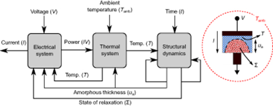
Figure 3. Block diagram of interconnections between electrical, thermal, and structural dynamics in a PCM device.
Download figure:
Standard image High-resolution image2.3. Applications of phase-change memory
2.3.1. Memory technology.
The memory hierarchy of conventional computing architectures is designed to bridge the performance gap between the fast central processing units (CPU) and the slower memory and storage technologies. A technology classified as storage is non-volatile (i.e. the stored data will be retained when the power supply is turned off) and low-cost, but has much slower access times than the CPU operations (figure 4). Storage technologies include NOR and NAND Flash, magnetic hard-drive disks (HDDs) and tape. Memory technologies on the other hand are volatile (the data is lost when the power supply is turned off) and more expensive than storage, but have much smaller access times. Memory technologies include the static random access memory (SRAM) used in the CPU caches and off-chip dynamic random access memory (DRAM).

Figure 4. Access times for various memory and storage technologies. Small amounts of expensive high-performance volatile memory sit near the CPU whereas vast amounts of low-cost yet slow storage are used to stock data. Currently there exists a gap in access times of about three orders of magnitude between memory and storage, which could potentially be filled by a so-called 'storage class memory'.
Download figure:
Standard image High-resolution imageThe use of PCM as potential DRAM replacement, as part of the main memory system, has been investigated in a wide variety of works for more than 10 years as of now [24–27]. At the time when the first investigations were performed (around 2009), DRAM had fallen behind NAND Flash and standard CMOS logic technologies in terms of scaling to the 45 nm technology node and preparation for the 32 nm node [13]. However, PCM had already been demonstrated to scale down to the 20 nm node [28]. Hence, PCM could compete well in terms of forward scaling for increasing main memory density and capacity due to challenges in making DRAM capacitors small and yet being able to store charge reliably. Those various studies conclude that if PCM can be produced at a higher density than DRAM, various architectural reorganizations of the main memory system could make PCM a viable alternative to DRAM in spite of the lower latency and finite endurance. Moreover, the non-volatility of PCM could be exploited in the main memory and would avoid the need to rewrite after each read access, which is unavoidable with DRAM [13]. However, at the time of writing, DDR4 DRAM technology has been scaled down to the 10 nm-class node, which denotes a process technology node somewhere between 10 and 19 nanometers [29]. Due to those recent advances in integrating DRAM into smaller nodes, it is currently unclear whether PCM will be able to displace such a stable and reliable technology.
Another potential application of PCM as a conventional memory technology is its use as so-called storage class memory (SCM) [30]. As seen in figure 4, there is currently a gap of three orders of magnitude between the access times of DRAM and of Flash. SCM aims at bridging this performance/cost gap between memory and storage, which could be made possible with PCM. SCM would blur the traditional boundaries between storage and memory by combining the benefits of a solid-state memory, such as high performance and robustness, with the archival capabilities and low cost of conventional hard-disk magnetic storage [13]. One variant of SCM could act as a fast solid-state drive (SSD) with better native endurance and write access times than the Flash-based SSDs. Access times in the order of 1 µs would be acceptable, but low cost via high density would be most important [13]. Another variant could have access times in the order of 100 ns with low-power and cost constraints. This would be fast enough to enable it to be connected to the usual memory controller [13]. SCM would likely not be as fast as DRAM, but its non-volatility could greatly reduce the amount of DRAM required to maintain a high bandwidth. In this way, the power consumption and hopefully the cost of the overall system would be reduced [13].
Besides using PCM as a standalone memory in a conventional computer system, another important emerging application domain for PCM is as embedded memory [31, 32]. Recent demonstrations include the integration of 6MB PCM in an automotive grade microcontroller chip [33]. Here, the advantage of PCM is that it can be integrated in the back end of the line, unlike the conventional Flash memory cells, which enables easier integration in advanced CMOS nodes [32]. PCM also offers superior write flexibility and speed with respect to Flash, and is well positioned with respect to other resistive memory devices in applications that require an extended temperature range (up to 150 °C) [32].
2.3.2. Non-von Neumann computing.
An additional key emerging application area for resistive memory devices such as PCM is that of non-von Neumann computing [34, 35]. In this novel computing paradigm, memory elements are not only used to store information but also execute computational tasks with collocated memory and processing at considerable speeds. For this, a low-power, multi-state, programmable and non-volatile nanoscale memory device is needed. Resistive memory devices (or memristive devices) that remember the history of the current that previously flowed through them, are promising candidates for this application. Memristive devices include PCM but also other emerging non-volatile memories such as resistive random access memory (RRAM), conductive bridge random access memory (CBRAM), or magnetic random access memory (MRAM) [36]. A significant implication of this concept is that the clear-cut distinction between memory and computing is blurred, which may lead to entirely new computational models and algorithms that would take advantage of non-von Neumann architectures.
Two non-von Neumann computing paradigms using memristive devices have recently emerged. In one approach, memristive devices are used for implementing neuromorphic computing systems. The aim is to perform machine learning tasks using a neural network system whereby the neurons and/or synapses composing the neural network are implemented with memristive devices. Another fascinating paradigm is that of in-memory computing, whereby the physical attributes and state dynamics of memristive devices are used for analog computing or to perform logic operations, without being tied to a neural network framework.
The feasibility to program single PCM devices to a wide range of different states (inherent to the working principle of PCM) is promising for non-von Neumann computing applications and has in fact been exploited in all experimental demonstrations using PCM to date [37–41]. Another key property of PCM is that the amorphous region can be progressively crystallized by applying repetitive electrical pulses [41, 42]. This accumulation property (in fact, the PCM integrates the electric current flowing through it) is essential for emulating synaptic dynamics [40, 43] and can also be used to implement some arithmetic operations [42, 44, 45]. Besides conventional electrical PCM devices, photonic PCM devices [46] which can be written and read optically, are being explored for all-photonic chip-scale information processing. Such a memory device has been recently employed for the analog multiplication of an incoming optical signal by a scalar value encoded in the state of the device [47]. Those promising characteristics indicate that PCM could potentially play a key role as the central element in a non-von Neumann computing system [48, 49].
3. Write operation
3.1. Thermal characteristics
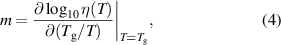
The operation of a PCM device is highly influenced by the temperature distribution achieved in the phase-change material when applying an electrical pulse to the device. In a typical mushroom-type PCM device (as depicted in figure 5), finite-element simulations indicate that the maximum temperature is reached very close to the bottom electrode [50–52]. This is due to the significant asymmetry between the dimensions of the top and bottom electrodes. The substantially smaller bottom electrode and hence higher current density ensure that most of the electric power is dissipated within the phase-change material close to the bottom electrode. This causes a rise in temperature, which will be balanced by the heat transport away from the device. By averaging over all possible heat pathways through materials with very different thermal conductivities and geometric contributions, an average thermal resistance  for the heat transported away can be defined.

Figure 5. Finite-element simulation indicating the temperature distribution in a mushroom-type PCM device upon application of a voltage pulse with power,  . The temperature close to the bottom electrode is referred to as the hotspot temperature,
  . The heat loss (indicated in green) can be modeled with an equivalent thermal resistance,
  , that captures the thermal resistance of all possible heat pathways. The PCM device is operated within ambient temperature,
  . Reproduced from [53]. CC BY 4.0.
Download figure:
Standard image High-resolution imageIf  is the 'hotspot' temperature corresponding to the region just above the bottom electrode in the device, as also shown by Boniardi et al [54], it is possible to write

where  is the input power and
  the ambient temperature. One particularly interesting point when applying increasing input power
  to a PCM device is the onset of the 'plugging' of the bottom electrode with amorphous phase change material. At this point, the first measurable increase in the resistance of the device will occur, and
  will be approximately equal to the melting temperature of the phase-change material. For this particular point,
  can be seen as a measure of the programming efficiency of the PCM device. That is, the higher
  , the lower the power needed to melt the phase-change material and therefore the more efficient the PCM device. Values of
  in nanoscale PCM can be higher than 1.5 K/µW [53].
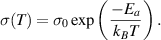
Because of the inhomogeneous temperature distribution, small dimensions, and high temperatures reached during SET and RESET in PCM, large temperature gradients will occur in the device. Those gradients lead to significant thermoelectric effects that will generate (or remove) heat in addition to Joule heating [23, 55–57]. The Thomson effect occurs when both a current density J and a temperature gradient ∇T are present in the device. The heat per unit volume predicted by the Thomson effect is  , where S is the Seebeck coefficient. This term represents the generation (or removal) of heat due to a current that passes through a gradient of the Seebeck coefficient resulting from a temperature gradient. A steady-state heat balance equation that incorporates this term can be thus written as
where κ is the thermal conductivity and σ the electrical conductivity of the phase-change material.  represents the heat transported away from the phase-change material. The first term is Fourier's heat conduction law, and the second term is the Joule heating.
The main impact of the thermoelectric Thomson effect on the operation of a PCM device is that the location of the hotspot will be shifted towards the anode (positive) contact [55]. The Seebeck coefficient in most phase-change materials such as Ge2Sb2Te5 is positive (the conduction is p-type) and has a negative temperature dependence, leading to a negative Thomson coefficient  . Therefore, if J is in the direction of the temperature gradient from the top electrode to the hotspot, the Thomson effect will generate additional heat that will push the hotspot away from the bottom electrode and expand the amorphous region [23, 56]. This results in less power required to achieve the onset of plugging when the polarity of the voltage drop is positive at the top electrode with respect to the bottom electrode. When the anode is the bottom electrode, the Thomson effect heat drain will push the hotspot further down into the bottom electrode, which will increase the plugging power because some of the input power will be dissipated within the electrode instead of the phase-change material. Discontinuities in the Seebeck coefficient at the interfaces with the phase-change material (especially the bottom electrode interface) will also generate (or remove) additional thermoelectric heat (Peltier effect) [23, 57]. The differences resulting from thermoelectric effects in the input power required to achieve the onset of plugging between positive and negative polarity can be more than 10% [56].
3.2. SET/RESET operation
The principles of crystallization and amorphization underlying the WRITE operation of PCM are illustrated in figure 6. In order to amorphize the phase-change material inside the PCM device (RESET), a high voltage or current pulse with sharp edges is applied. The resulting power dissipation must be high enough such that, through Joule heating, the temperature within the PCM device reaches values above the melting temperature,  , of the phase-change material. The induced melting erases any periodic atomic arrangement that was previously created. Once the phase-change material is molten, it must rapidly be cooled down (or quenched) in order to 'freeze' the atomic structure into a disordered state. If the regime of fast crystallization (see figure 6) is rapidly bypassed by fast quenching, the atomic mobility at temperatures below this regime becomes so small that the atoms cannot rearrange and find their most energetically favorable configuration during cooldown, and are thus frozen into a non-equilibrium (or 'glassy') amorphous state. This process is commonly referred to as glass transition and leads to the creation of the amorphous (high-resistance or RESET) state. The amorphization process can be as fast as a few tens of picoseconds, thanks to the fast melting kinetics of PCM [59], with the phase-change material typically molten at temperatures greater than ∼1000 K [60].

Figure 6. Principles of a WRITE operation in PCM. A RESET brings the PCM device to a high-resistance state via amorphization of the phase-change material by heating above the melting temperature  and subsequent rapid cooling of the material. A SET brings the PCM device to a low-resistance state via crystallization of a previously amorphous region. The size of the amorphous region can be modulated by changing the pulse power amplitude. Based on [58].
Download figure:
Standard image High-resolution imageIn order to switch from the amorphous to the crystalline state (SET), a voltage or current pulse is applied to bring the temperature within the PCM device to a temperature inside the regime of fast crystallization. Moreover, the length of the pulse has to be long enough so that complete crystallization of any previously created amorphous region occurs. This process leads to the creation of a crystalline (low-resistance or SET) state. The crystallization process typically takes much longer than the amorphization process, around tens to hundreds of nanoseconds, and crystallization is realized at temperatures typically above ∼500 − 600 K but below  [60].
[60].
3.2.1. Crystallization kinetics.
The crystallization speed of PCM depends on the volume of initially amorphous material that is going to be crystallized and the crystallization kinetics of the phase-change material used, which are highly temperature dependent. The crystallization kinetics of PCM at elevated temperatures can be either nucleation or growth driven, and has been (and continues to be) a topic of intense research [53, 60–69]. Nucleation is a stochastic process in which a crystalline nucleus eventually reaches a critical size beyond which it is stable, such that it can grow rather than dissolve. The build-up of the critical size nucleus requires an incubation time. The critical size depends on the temperature and is determined by the bulk free energy difference between amorphous and crystalline phases (reduces the critical size when it increases) and the interfacial energy density between amorphous and crystalline phases (increases the critical size when it increases). Crystal growth occurs when the nucleus reaches the critical size, and is a deterministic process. The crystal growth velocity is highly temperature dependent and determined by the free energy difference between liquid and crystalline phases (increases growth velocity when it increases) and the viscosity (decreases growth velocity when it increases).
In conventional conditions such as those for optical disks, it has been shown that crystallization in AIST is growth-driven (slow nucleation), and in GST it is nucleation-driven (fast nucleation) [60]. However, it has been argued that in nanoscale PCM devices, the role of nucleation may be less important and crystallization may be governed mostly by crystal growth [53, 70]. Unlike crystal growth, there is a temporal dependence on the nucleation rate to reach the steady-state rate (typically characterized by an incubation time) [71]. If the growth rate is sufficiently high for significant growth at the amorphous-crystalline interface (see figure 6) to occur before the incubation time for nucleation is reached, the crystallization will be growth-driven even in nucleation-dominated phase-change materials [72]. This is especially true in nanoscale PCM mushroom cells, where the ratio between the amorphous-crystalline interface area and the volume of the amorphous region is very large. A second argument in favor of the dominance of crystal growth over nucleation in PCM devices is given by Lee et al [70]: the melt-quenched amorphous phase of GST is expected to already contain a large number of quenched-in crystalline nuclei that are developed during the cooling time upon RESET. Therefore, even if new nuclei may develop during the crystallization process, growth of the already existing quenched-in nuclei may likely dominate the total crystallization time.
A widely accepted model describing the temperature dependence of crystal growth is [64]
where  is the atomic radius, λ is the diffusional jump distance,
  is the hydrodynamic radius,
  denotes the Boltzmann constant and T is the temperature. The term in the square brackets captures the thermally activated atomic transfer across the solid-liquid interface. ΔG(T) is the Gibbs energy difference between the liquid and the crystalline phase and serves as the driving force for crystallization. Different expressions for ΔG(T) exist in the literature. In general, ΔG(T) will be larger than 0 for
  (i.e. the crystalline phase is energetically more favorable than the liquid phase), equal to 0 at
  , and smaller than 0 for
  (i.e. the liquid phase is more favorable than the crystalline phase). The expression for ΔG commonly used for phase-change materials is the Thompson–Spaepen approximation, [73] which was also employed by Orava et al [74] and Salinga et al [64]
where  is the heat of fusion.
In equation (2), η(T) denotes the viscosity. It is the physical quantity that limits the crystallization process, counteracting the driving force, and that is coupled to the atomic diffusivity through the Stokes–Einstein equation. As the molten phase-change material is being cooled below the melting temperature (in the so-called super-cooled liquid state), the viscosity steadily increases with cooling, and it becomes increasingly difficult to sample all possible configurations for a given temperature. Eventually, the liquid falls out of internal equilibrium and forms a glass [75]. This process is expected to depend on the cooling rate: at slower cooling rates, the system will remain in internal equilibrium longer than for faster cooling [76–79]. Whether the material is in the glass state or in the super-cooled liquid state will influence the temperature dependence of the viscosity [80]. In the glass state, the viscosity usually shows an Arrhenius-type temperature dependence, i.e. it is proportional to  with activation energy
  . In the super-cooled liquid state, a more or less pronounced deviation from the Arrhenius-like temperature dependence is observed depending on the material. Super-cooled liquids with approximate Arrhenius behavior are called strong, whereas those which strongly deviate from an Arrhenius behavior are called fragile [81]. A common measure of this deviation from the Arrhenius behavior is the so-called fragility m, given by
where  is commonly defined as the temperature at which viscosity equals 1012 Pa-s [82]. Fragilities reported in literature range from 20 for very strong liquids like SiO2, up to over 150 for some very fragile, typically organic, polymers [64, 82].
Many works have attempted to experimentally measure the growth velocity as a function of the temperature in different phase-change materials, both in the amorphous as-deposited state [61, 62, 65, 83], and in the melt-quenched state of memory cells [53, 64, 84]. Investigations of the crystallization process are also being pursued using ab initio molecular dynamics simulations by several groups [85–87]. From equation (2), it is predicted that the growth velocity at low temperatures increases as a function of temperature up to a value at which the crystallization rate is maximum. For temperatures higher than the temperature at which the growth rate is maximum, the growth velocity decreases when increasing the temperature until  , at which the growth velocity becomes 0. Most of the direct experimental measurements have been performed in the low temperature regime, that is when temperature is lower than the temperature of maximum crystallization. An Arrhenius-type temperature dependence has been commonly reported, spanning more than eight orders of magnitude of growth velocity, up to high temperatures typically above 500 K [53, 64, 65, 68, 84]. Indirect experimental measurements made it also possible to infer values of the maximum crystallization temperature, typically between 600 K and 800 K, where the growth velocity can reach values higher than 1 m s−1 [53, 88].
One point that remains debated is whether the wide Arrhenius-type temperature dependence of the growth velocity measured at low temperatures occurs in the glass or super-cooled liquid state. For the former, the resulting fragility values in the super-cooled liquid typically have to be very high (> 100) to explain the experimental data [53, 64, 88]. For the latter, the Arrhenius-type behavior over a wide temperature range has recently been explained as the result of a fragile-to-strong crossover in the super-cooled liquid in order to capture experimental observations [65]. These contradicting interpretations mainly result from the fact that it is quite difficult to obtain a precise measure of the glass transition temperature in phase-change materials. For example, for GST, a wide range of values of the glass transition temperature have been reported between 100 °C and 200 °C [89]. Recent measurements have attempted to resolve this point for GST and a glass transition temperature of 200 °C was experimentally reported by differential scanning calorimetry [89]. This would rather indicate that the wide Arrhenius-type temperature dependence occurs mostly in the glass phase in this material. Further investigations on the role of structural relaxation, which is expected to affect the viscosity [64], are also needed in order to better understand its impact on the crystallization kinetics when operating PCM cells. In fact, structural ordering has been shown to significantly affect crystal growth in metallic glasses [90], and similar effects are expected to be relevant for PCM as well.
When crystallizing PCM using electrical pulses, the temperature distribution in the device (see figure 5) plays a crucial role in the crystallization dynamics [53]. For a different pulse amplitude, a different temperature distribution will be achieved in the device. Therefore, depending on the size of the initial amorphous region and the pulse amplitude, crystallization can occur inside the amorphous region, at the crystalline-amorphous interface, or both. The inhomogeneous temperature distribution therefore imposes some limits on which parts of the amorphous region can crystallize with a given pulse. For example, a low amplitude pulse is likely to crystallize only inside the amorphous region close to the bottom electrode, whereas a high amplitude pulse may crystallize only close to the crystalline-amorphous interface (because the temperatures reached inside the amorphous region may be too close to the melting temperature for which the crystallization rate is very small). A rather straightforward way to ensure total crystallization of the amorphous region is to apply a pulse with a long training edge, such that the temperature at which the crystallization rate is maximum will be achieved all over the amorphous region for some time.
Although most studies have focused on crystal growth in melt-quenched PCM, precisely understanding the role of nucleation in PCM cells would be important as well. Even if it is possible to describe experimental data mostly with a solely growth-based crystallization mechanism, it is not expected that nucleation does not have any influence in all experimental conditions. Especially when applying low-power voltage pulses to crystallize a PCM mushroom-type cell, it is possible that the higher temperatures reached in the middle of the amorphous region could induce nucleation there. An interesting avenue to study the influence of nucleation could be to treat the melt-quenched amorphous dome with some low-energy pulses which would not crystallize it, but would vary the density of crystalline nuclei inside the amorphous region [70]. It has been shown experimentally that such pre-treatment can indeed result in a faster crystallization speed in PCM cells [91].
3.2.2. Multi-level operation.
A key property of a PCM device is that the size of the amorphous region can be altered in an almost completely analog manner by applying suitable electrical pulses. This is a consequence of the inhomogeneous temperature distribution within the PCM device. In the mushroom-type PCM device depicted in figure 6, the highest temperature reached through Joule heating, resulting from an electrical pulse, is typically close to the bottom electrode. Therefore, by applying a RESET pulse that dissipates more power, a bigger amorphous region is created because  is reached further away from the bottom electrode. This bigger amorphous region will result in a higher resistance of the PCM device. By exploiting this property, one can therefore code more than 1 bit of information in a single PCM device because a continuum of resistance states can be achieved, each of which can represent a certain bitstream (e.g. '11', '10' etc.). One can also vary the width of the pulse (for SET) or the length of its trailing edge to program multiple resistance levels. The mapping between PCM resistance and programming power is typically referred to as programming curve. One such typical programming curve obtained with a mushroom-type PCM device initially in the RESET state is shown in figure 7. The left part of the programming curve is unidirectional as it mostly involves an amorphous-to-crystalline phase transition (e.g. it is not possible to have crystalline-to-amorphous phase transition in this part of the curve). The right part of the programming curve is mostly bidirectional, with the melt-quench process dominating the phase transition (e.g. both crystalline-to-amorphous and amorphous-to-crystalline phase transitions can be realized in this part of the curve). Reliable multi-level storage with PCM has been demonstrated for up to 3 bits (8 levels) per memory cell [92].

Figure 7. Low-field resistance as a function of the applied programming power (programming curve) for a PCM device initially in the RESET state. Box pulses of increasing power amplitude with 7.5 ns edges and 200 ns width are applied. In the left part of the programming curve, the initially created amorphous region progressively crystallizes until the low-field resistance reaches a minimum value. In the right part of the programming curve, an amorphous region of increasing size is formed, resulting in an increase of the resistance with increasing programming power.
Download figure:
Standard image High-resolution image3.3. Threshold switching process
In order for the above crystallization/amorphization scheme to be of practical use for electrical data storage using PCM, the ability to rapidly increase the temperature strongly within the device independently of the resistance state is needed. In optical storage, this is easily achieved by heating the phase-change material with a laser source of sufficient power regardless of the state of the material. In PCM, a key property that enables fast substantial power dissipation by the application of a relatively low voltage pulse whose amplitude is mostly independent of the resistance state is a highly non-linear current/voltage (I–V) characteristic. Typical I–V characteristics of the amorphous and crystalline states are represented in figure 8. While the crystalline state has a fairly ohmic behavior at low voltages, the variation of the current with applied voltage in the amorphous state is highly non-linear. In the so-called amorphous OFF state (or subthreshold regime), the current shows an ohmic, exponential, and super-exponential behavior with increasing applied voltage. Beyond a certain voltage  , called threshold switching voltage, the conductivity of the amorphous phase increases rapidly via a feedback-driven mechanism resulting in a negative differential resistance (voltage snapback). If the device current is measured in voltage mode as shown in figure 8, the observed negative differential resistance will typically be that of the load resistor
  used in series with the PCM device to limit the current, because the PCM resistance typically decreases below
  upon threshold switching. When PCM is operated in an array, the negative differential resistance will be controlled by the nonlinear selector device or transistor in series with the PCM. The state reached upon threshold switching is typically called amorphous ON state, because the amorphous phase has not yet crystallized. Once sufficient current passes through the PCM device in the amorphous ON state for a sufficiently long time, memory switching (total crystallization) occurs and the amorphous ON state I–V characteristic merges with that of the crystalline state.

Figure 8. Quasi-static switching I–V characteristic of a PCM device initially in the amorphous state measured in voltage mode (see inset). A triangular voltage ramp is applied to the PCM device in series with a load resistor  kΩ, and the voltage drop across
  is subtracted from the applied voltage to obtain the PCM I–V characteristic. Upon reaching
  , threshold switching occurs and the current quickly increases, leading to a voltage snapback. The measured negative differential resistance is that of
  because the device resistance drops below
  upon threshold switching. Memory switching (total crystallization) occurs when the amorphous ON state I–V characteristic merges with that of the crystalline state. The dashed green line shows the continuation of the I–V characteristic starting from the crystalline state when applying higher voltages, for which the phase-change material gets heated up to high temperatures and eventually melts.
Download figure:
Standard image High-resolution imageThe origin of the threshold switching mechanism in PCM is a long standing debate which is still not resolved despite the fact that the phenomenon was first observed more than 50 years ago by Ovshinsky [93, 94]. A large number of models have been proposed to explain threshold switching in PCM [3], which can be broadly classified as either thermal (i.e. the switching is associated with an electro-thermal instability occurring in the device) [95–101] or purely electronic [50, 102–110].
3.3.1. Thermal models.
Thermally-initiated switching will occur when the temperature increase within the device due to Joule heating induces a significant conductivity increase due to thermal activation of carriers. A positive feedback loop will be established, resulting, as the conductivity increases, in increased power dissipation in the device, which in turn will lead to a further increase of the conductivity. This can trigger the onset of an instability in this highly nonlinear feedback system, leading to a negative-differential I–V characteristic.
This electro-thermal instability was the first mechanism proposed to explain threshold switching in phase-change materials [111]. The condition for thermal breakdown was first formulated by Wagner in 1922 [3, 112]. He considered a dielectric film of thickness L, whose conductivity depends on temperature as
Wagner assumed that the breakdown occurs in a weak region in the form of a thin filament with a cross section S and that heat was only released within the filament. Assuming that the temperature is independent of the coordinates and that the temperature of the region outside the filament is constant and equal to the ambient temperature, the steady-state heat balance equation is written as
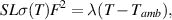
where F is the electric field, λ is the heat exchange coefficient in WK−1, T is the filament temperature and Tamb is the ambient temperature. By solving  for the above equation one obtains the threshold temperature Tth at which the I–V becomes negative differential
where the approximation holds for  . For
. For  , the negative differential behavior is absent. The electric field Fth corresponding to this condition is given by
For non steady-state breakdown, the heat balance equation takes the form
where ρ is the density and C is the specific heat.
When a field-dependence is introduced in the conductivity, i.e. σ(F, T), the model is commonly referred to as electro-thermal because along with the thermal effects, electronic processes leading to a field dependence of the conductivity are considered. Such electro-thermal models have been proposed to explain threshold switching in chalcogenide glasses in the 1970s by Boer [95], Warren [96], Kroll [97] and Shaw [98]. However, they were mostly discarded in the 1980s in favor of an electronic excitation mechanism [104]. Nonetheless, thermally initiated switching was recently reconsidered when dealing with nanoscale PCM devices, in which self-heating effects were shown to play a significant role [101, 113, 114].
3.3.2. Electronic models.
Other purely electronic mechanisms were proposed in the 1970-1980s to explain threshold switching in semiconducting glasses. The most notable ones are the double-injection model by Mott [102] and Henisch [103] and the generation-recombination model of Adler [104]. Most of the experimental work at that time was done on thin films, typically with large thermal time constants, and a debate over the thermal versus electrical origin of threshold switching was settled mostly in favor of the latter [104]. In the past 10 years, those electronic models have been revived and modified to explain data measured in nanometric PCM devices [50, 105]. Moreover, new models have been developed to explain threshold switching via a wide variety of different mechanisms, such as tunneling between trap states [106], energy gain via carrier temperature increase [107, 108], field-induced nucleation [52, 109], or quantum percolation [110].
3.3.2.1. Double-injection model.
One of the first electronic models for the switching effect was the double-injection model proposed independently by Mott [102] and Henisch [103]. They assumed that when a voltage is applied between the electrodes contacting the device, electrons and holes are injected from the cathode and anode respectively. Then, injected carriers recombine in the bulk. At first, electrons recombine close to the cathode and holes close to the anode, creating a negative and positive space-charge at the cathode and anode, respectively. With increased voltage, the space-charge regions grow from the electrodes and neutralize each other when they overlap. This makes the electric field collapse in the center, and the voltage drop then occurs in a narrow region near the contacts. The small thickness of the formed barriers allows electrons and holes to tunnel into the material bulk rather easily. At this point, a quasi-metallic conductivity is obtained because of the large charge density in the bulk and thus the material has switched. An obvious consequence of this model is that the voltage required to hold the switched on-state must be approximately equal to the bandgap and independent of the device thickness [3]. However, there are open questions regarding how the Schottky-type barriers at the electrodes can be maintained [115]. Moreover, because of the space-charge dominated transport process, the threshold switching voltage would be expected to be a function of the square of the thickness (or electrode separation) [116], which is not observed in phase-change devices [117].
3.3.2.2. Generation-recombination model.
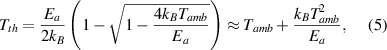
The generation-recombination model of Adler [104] is based on the valence-alternation pair (VAP) defect model that had been proposed for amorphous chalcogenides [118, 119]. In the presence of such defects, carriers will undergo generation and recombination events with different time constants for each of these processes. When the generation rate monotonically increases with the electric field and is proportional to the number of carriers, such as for impact ionization, it was shown that threshold switching can occur under isothermal conditions. To obtain the conductivity at a given electric field, a set of kinetic equations for electrons and holes as well as for the defect centers have to be solved. The total generation rate for electrons and holes consists of the sum of a thermal generation Gtherm and a field-dependent generation G which is assumed to be proportional to the carrier concentration as well as to a monotonically increasing function of the electric field g(F). A simplified solution to this model can be derived in the off-state where the free carrier concentration is much smaller than the concentration of trapping centers and considering only one carrier type (p). The steady-state balance between generation and recombination in a homogeneous system can be written as

where τp is the characteristic hole capture time and  . Because G = pg(F), the solution to this equation is given by
The electric field Fth satisfying the condition  is thus the field at which threshold switching occurs. The same set of kinetic equations can be used to describe the post-switching on-state, in which the concentration of free electrons and holes is now larger than the concentration of trapping centers. Pirovano et al showed good agreement of this model with experimental data on nanoscale PCM cells [105] and further simplified it by assuming that recombination occurs in a single type of defect centers [50], thus extending the validity of the model beyond the VAP hypothesis to any type of system with defect states that act accordingly (in their case donor-like traps). However, the validity of using an impact ionization type of generation mechanism in amorphous semiconductors, where the mean free path is very small, has been questioned [3, 120].
3.3.2.3. Tunneling between trap states.
In the first model by Ielmini [106], it is proposed that Fowler–Nordheim tunneling from deep traps to shallow traps leads to an instability at high-fields, when the tunneling current becomes larger than the thermally activated current. Essentially, a conduction model is used to describe the electron current due to the Poole–Frenkel effect (see section 4.1) from two trap states (shallow and deep), and it is assumed that electrons can tunnel from the deep to the shallow trap state, thus increasing the trapped electron concentration in the shallow trap state. Therefore, the quasi-Fermi level for electrons moves towards the conduction band. Similar to the double-injection model, injection via Fowler–Nordheim tunneling is believed to start from the electrode. The high conductive on-state region (with excess electron concentration in the shallow trap state) eventually fills up the whole active volume of phase-change material. While this model indeed yields a negative-differential I–V characteristic, it predicts that the threshold voltage increases with increasing temperature [106], which is the opposite of what is observed experimentally in phase-change materials. This is because the current due to nonequilibrium carriers in the shallow level needs to be larger than the thermally activated (equilibrium) current in order to produce an instability that can lead to switching.
3.3.2.4. Hot-carrier model.
In the second model by Ielmini [107], later reworked by Jacoboni et al [108], a hydrodynamic-like approach is used. Hereby, a Fermi distribution function incorporating a quasi-Fermi level and a carrier temperature replaces the equilibrium Fermi distribution. The energy-balance equation is solved assuming a relaxation time constant τR for the rate of energy exchange between carrier and lattice. The model also includes the associated equation for the current density (using a Poole–Frenkel description of the electrical conductivity, see section 4.1) and the Poisson equation introduced by Jacoboni et al to take into account the variation of the carrier density along the device, which was not considered in the original work of Ielmini. In this model, the dissipated power σF2 is assumed not to heat the lattice but instead to raise the carrier temperature and shift the quasi-Fermi level away from the equilibrium Fermi level. Thus, the threshold temperature Tth at which switching occurs is identical to that of the thermal instability model (equation (5), assuming coordinate independence and ohmic conduction) [121]. However, this temperature does not correspond to the filament temperature but to the carrier temperature. The main shortcoming of this model at the moment is that it fails to explain the experimentally measured switching delay times, which have been reported in the range of a few nanoseconds up to as much as 1 ms [122]. The carriers heat up with a time constant of τR, which should realistically be in the order of 10−13 s [123]. Assuming such a time constant, the predicted intrinsic delay times would range from a few to tens of ps [124]. A possible explanation for this discrepancy could be that the experimentally observed longer delay times would be dominated by parasitic components of the device and of the control electrical circuit [125]. An additional difficulty is that a rigorous proof of the validity of the hydrodynamic transport theory in amorphous semiconductors is yet to be established.
3.3.2.5. Field-induced nucleation.
The field-induced nucleation model of Karpov [109] considers that the crystallization energy barrier decreases upon application of an electric field, therefore a cylindrical crystal nucleus is formed rather rapidly in a high electric field. Therefore, an electric field can create a crystalline filament that can grow from one electrode to the other in a certain delay time. Once the filament connects the two electrodes the device has switched. If the field is removed, the filament will either disappear or grow depending on whether its radius is smaller or larger than the minimum thermodynamically stable radius. The case where the filament is thermodynamically stable describes memory switching, otherwise the reverse transition to the off-state occurs. The model has been shown to quantitatively describe the temperature and applied voltage dependence of the switching delay time [126]. However, there is some controversy about whether a set of realistic physical parameters in this model can lead to threshold switching at the experimentally measured electric fields [52].
3.3.3. Experimental characterization.
The threshold switching characteristics of a PCM device depend on many parameters. A critical dependency is the variation of the threshold voltage with respect to the programmed resistance state. A representative measurement of the dependence of the threshold switching voltage and current as a function of the current used to RESET the PCM device is shown in figure 9. It can be seen that the threshold voltage monotonically increases with increasing RESET current, hence with increasing size of the amorphous region. The threshold current at which the device switches decreases with increasing RESET current until it stabilizes to a fairly constant value around 10 µA. The threshold voltage has a negative temperature dependence and can decrease by a factor of almost two when the temperature increases from room temperature to 120 °C [101]. The threshold voltage also increases as a function of time, due to structural relaxation of the amorphous phase that is also responsible for the resistance drift phenomenon (see section 4.2). The variation over time can be significant as well; a > 25% increase in threshold voltage can be observed over six orders of magnitude in time at room temperature, and this increase is accelerated as the temperature increases [101]. This has important ramifications for technological applications, because over time the threshold voltage could rise above the maximum voltage that can be supported by the programming circuitry of a PCM chip.
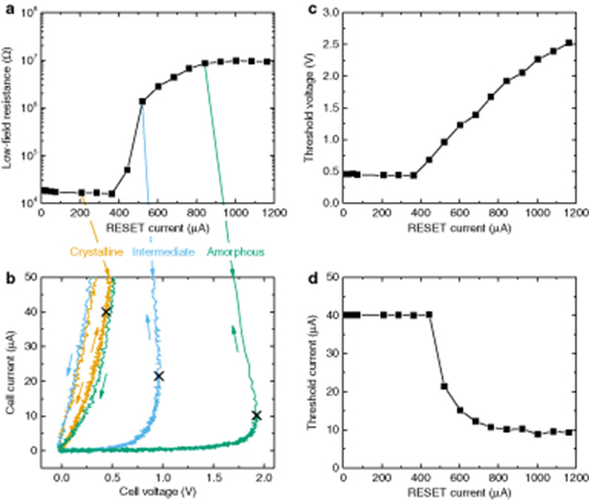
Figure 9. (a) Change in low-field resistance when applying progressively higher RESET currents. (b) Measured I–V characteristics after RESET for three different resistance states of (a). The black crosses denote the point of maximum cell voltage of the I–V characteristics. (c) Threshold switching voltage and (d) current as function of the RESET current. For the crystalline states where no voltage snapback is observed, the threshold voltage is defined as the voltage at which the current reaches a value of 40 µA. Data reproduced from [101].
Download figure:
Standard image High-resolution imageAnother critical aspect of threshold switching is the temporal dynamics occurring in the PCM current and voltage response when a switching pulse is applied to it. One particularly important aspect of these dynamics is the so-called switching 'delay time', that is the time it takes for the device to switch while a voltage pulse is applied. The delay time reduces exponentially with the applied voltage, as commonly observed in many types of resistive memories such as RRAM [93]. Experimentally reported delay times in PCM range from a few nanoseconds up to as much as 1 ms [101, 122]. A representative experimental measurement of the delay time as a function of the applied voltage in nanoscale PCM is shown in figure 10. The delay time measurement was done by applying a box pulse with sharp leading and trailing edges of 7.5 ns. The voltage amplitude of the pulse was varied, and the time delay between the application of the voltage pulse and the sharp rise of current was monitored. The typical exponential dependence on the applied voltage is observed for voltages higher than the 'steady-state' threshold switching voltage (dotted line in the simulation shown in figure 10(a)). At this voltage, the delay time increases asymptotically and the device will not switch for applied voltages somewhat below it. The current traces shown in figure 10(b) indicate that the current increases slowly over the delay time duration until a sharp rise occurs [122]. The long delay time events of more than 1 µs observed experimentally exhibit significant randomness, which suggest that they could be due to fluctuations (either thermal or electrical) or small variations in the initially created RESET state. Such stochastic behavior for long delay times has also been reported in the literature [104, 127–129].

Figure 10. (a) Measured delay time as a function of the applied voltage. (b) Current traces as function of time, obtained for three different applied voltages. The simulations shown along with the experimental data were performed with the thermally-assisted threshold switching model presented in [101]. Data reproduced from [101].
Download figure:
Standard image High-resolution imageThe fact that so far no unique mechanism has been proven to quantitatively capture all commonly observed features of threshold switching across all different materials and devices in a unified way more than 50 years after the phenomenon was first reported in phase-change materials suggests that likely many different mechanisms play a role. Clearly, many studies on chalcogenide devices (mainly thin films) in the past have shown incompatibilities with a solely thermal switching mechanism [104, 128, 129]. Especially in thin films, the question whether a thermal or electronic threshold switching mechanism dominates still remains open. Surprisingly fast switching times (sub-nanoseconds) have recently been observed in thin films of AIST phase-change material [130], which may put into question whether a thermal switching mechanism can explain threshold switching in such devices. However, we note that switching times down to 10–100 ps have been shown to be accounted for by purely thermal processes in nanoscale vanadium sesquioxide devices [131]. Thus, thermal processes can be expected to lead to very fast switching in nanoscale devices, or when switching is filamentary or self-accelerating, both being effects that can significantly reduce thermal switching times. Recent simulations confirming this statement have been performed by Bogoslovskiy and Tsendin [114]. Regarding the electronic models, a thorough quantitative comparison with experimental data of the different approaches, with both static and dynamic measurements, is lacking in order to exclude certain theories. Since all models can qualitatively reproduce some features of threshold switching, only quantitative matching with experimental data across a wide range of temperature and time can help in discriminating between the different approaches. Based on these considerations, we believe that at the present time it is certainly not unreasonable to assume that threshold switching is the combined result of many different physical mechanisms occurring at high fields, some of which could be more prominent in certain device geometries or materials. Depending on the device structures, functional materials, or switching conditions, some mechanisms might be more prominent than others, and understanding how they interact will likely yield significant insight. Further research into decoupling the thermal effects from the purely electronic ones in experiments is likely needed in order to make progress in this direction.
3.4. Write stochasticity
Here, we focus on the stochasticity of the PCM switching process, namely, the threshold switching and the crystallization process. The native switching stochasticity of PCM can be exploited, in particular, for population coding in spiking neural networks [132], or for random number generation for stochastic computing or cryptography [133, 134]. The essential property that is used in all those applications is the fact that, when applying a particular pulse to an array of PCM devices, the devices will switch with a certain probability p (0 ≤ p ≤ 1), and p can be modulated by changing either the pulse amplitude or the pulse width.
3.4.1. Threshold switching stochasticity.
Figure 11(a) shows representative measurements of the stochasticity of the threshold switching delay time on a single PCM device [133]. This delay time represents the time it takes for the current to rise steeply after the application of a voltage pulse. Therefore, the PCM will switch only if the width of the applied voltage pulse is greater than the delay time. In the experiment, after each RESET operation, a voltage pulse with an amplitude slightly above the steady-state threshold switching voltage is applied to the PCM device. It can be seen clearly that each experiment results in a different current trace and thus a different delay time. For a more detailed characterization of this randomness, we obtained delay time measurements 500 times for three pulse amplitudes of 1.8, 1.9 and 2 V. The results are shown in figure 11(b). The delay time random variable was found to roughly follow a log-normal distribution in all three cases. A simulation using the model described in [101] was able to capture the experimentally measured distributions well by introducing a small (0.5%) randomness in the amorphous thickness and activation energy of the device after RESET. It indicates that the stochasticity observed in the threshold switching process can be explained by variations in the atomic configurations of the amorphous phase created upon each RESET process. When using the threshold switching stochasticity in practical applications, one can tune both the pulse width and pulse amplitude to make the device switch with a given probability p.

Figure 11. (a) Experimentally measured current traces for a delay time experiment with a voltage pulse amplitude of 1.8 V repeated 20 times. The PCM device is RESET in between each delay time measurement. (b) Experimental and simulated delay time distributions from 500 measurements for three different applied voltages. Data from [133].
Download figure:
Standard image High-resolution image3.4.2. Memory switching stochasticity.
A second source of stochasticity in the PCM switching process arises from the crystallization process. In the nanoscale mushroom-type PCM device depicted in figure 1, the crystallization mechanism is assumed to be mainly dominated by crystal growth due to the large amorphous-crystalline interface area and small volume of the amorphous region. Moreover, for large enough pulse amplitudes, the temperature distribution reached within the device when a voltage pulse is applied also favors crystal growth at the amorphous-crystalline interface. Although crystal growth is a deterministic process, small variations in the atomic configurations of the amorphous volume created upon RESET can lead to variations in the effective amorphous thickness initially created. This, in turn, leads to a stochastic behavior of the crystallization time of a PCM device. An experiment that measures the stochasticity in the PCM crystallization time is shown in figure 12 [133]. In the experiment, a PCM device is first RESET and then a sequence of SET pulses is applied to the device. The amplitude of the crystallizing pulses is substantially larger than the threshold switching voltage to avoid any delay time stochasticity as well as to provide sufficient current to induce Joule heating and crystal growth. After the application of each crystallizing pulse, the low-field electrical resistance is measured. Experimentally measured traces of the resistance as a function of the number of crystallizing pulses for a constant pulse width of 50 ns are shown in figure 12(a). It can be seen that the resistance decreases incrementally upon the application of the pulses until it reaches its lowest value when the whole amorphous region has crystallized. Moreover, the resistance trajectories are different in each experiment, leading to a randomness in the total number of pulses needed to fully crystallize. In figure 12(b), we report the distributions of the number of pulses needed to crystallize  for different pulse widths. As for threshold switching, a simulation was able to capture the experimentally measured distributions well by introducing a 0.5% randomness in the amorphous thickness, using the model presented in [53] to capture the crystallization dynamics in the PCM device. Based on these distributions, the number of pulses
  can therefore be adapted such that the device will switch with a given probability p for a certain pulse width.
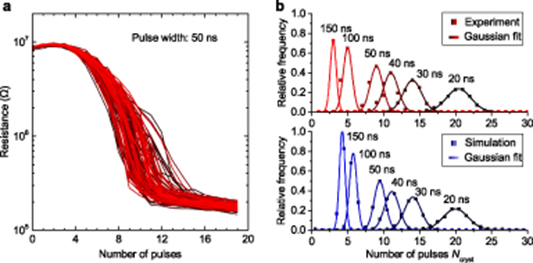
Figure 12. (a) Experimentally measured resistance as a function of the number of crystallization pulses applied for a fixed pulse width of 50 ns. The experiment was repeated 100 times and the device was RESET in between each experiment. (b) Experimental and simulated  distributions from 1000 measurements for six different pulse widths. Data from [133].
Download figure:
Standard image High-resolution image4. Read operation
The READ operation in PCM typically consists of reading the resistance of the PCM device through the application of a low voltage pulse. The READ voltage has to be lower than the threshold switching voltage so that it does not perturb the state of the device. Typical I–V characteristics of three different resistance states are shown in figure 13(a). They indicate that the low-field resistance increases and the slope of log(I) versus V decreases with increasing size of the amorphous region. However, a key challenge for retrieving the stored information is the resistance variations with time and temperature. These resistance variations are caused mostly by the phase-change material in the amorphous phase. Typical low-field resistance measurements for different resistance states at room temperature are shown in figure 13(b). It can be observed that the resistance increases over time, which is typically referred to as resistance drift. Resistance drift makes it difficult to reliably detect the different resistance states of PCM over time. What is also observed are significant fluctuations of the resistance over time for the higher resistance states. This noise, mostly attributed to the amorphous phase, is another key challenge for multi-level storage. In the following sections, the PCM resistance dependence on voltage and temperature, resistance drift, and noise will be described.
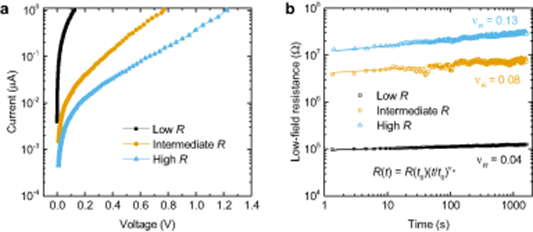
Figure 13. (a) I–V characteristics of three different resistance states (low, intermediate, and high). The low-field resistance increases and the slope of log(I) versus V decreases with increasing size of the amorphous region. (b) Resistance as a function of time for three different resistance states (low, intermediate, and high).
Download figure:
Standard image High-resolution image4.1. Subthreshold electrical transport
4.1.1. Temperature dependence.
In disordered materials, electrical transport occurs either via localized states through quantum-mechanical tunneling or via extended states dominated by trapping and release events (trap-limited band transport or multiple-trapping) [115]. In several amorphous phase-change materials, it has been shown that multiple-trapping can successfully describe the low-field conductivity measurements at temperatures above approximately 200 K, whereas at lower temperatures tunneling in localized states dominates transport [135, 136]. This is mainly motivated by the fact that in most of the commonly used amorphous phase-change materials, the activation energy for conduction at room temperature and above is close to half of the optical bandgap [137, 138]. This activation energy is typically in the range of 0.2 eV to 0.4 eV for amorphous PCM.
In the multiple-trapping picture, the conductivity comes solely from the free electrons and holes at or beyond the mobility edges. Once electrons are excited into the conduction band they can be accelerated by an electric field with a certain mobility µn. In addition, the holes in the valence band can also move with a certain mobility µp. The conductivity is then determined by counting the number of free electrons n and holes p in conduction and valence band respectively that carry the electric charge e.
The numbers of free electrons n and holes p in the bands are given by the Fermi–Dirac statistics. Therefore, the conductivity essentially depends on the position of the Fermi level with respect to the mobility edges.
The difference between conventional band transport and multiple-trapping is that, in the latter case, the position of the Fermi level will be significantly influenced by the presence of the localized states. In disordered materials, small variations in bond length and bond angle to neighboring atoms smear out the band edges and create band tails that decay exponentially into the bandgap. Those band tails are formed of localized states, i.e. the wavefunctions decay exponentially with distance. In addition to the band tails, other localized defects, namely shallow (close to one of the band edges) and deep (close to the middle of the bandgap) Gaussian-shaped trap states may be present in amorphous semiconductors. Shallow traps usually act as donor or acceptor levels, which increase the conductivity of semiconductors. In contrast, deep traps in most cases decrease the conductivity by pinning the Fermi level in the middle of the bandgap and by acting as centers for recombination of electrons and holes. Recent steady-state photoconductivity (SSPC), modulated photoconductivity (MPC) and photothermal deflection spectroscopy (PDS) experiments showed that both band tails and Gaussian trap states are present in amorphous GeTe [139]. From those measurements it was inferred that the conduction band tail is wider than the valence band tail in GeTe, which causes the transport to be dominated by holes at high temperatures. Hole conduction (p-type) was also confirmed by a positive Seebeck coefficient (or thermopower) measured in most amorphous phase-change materials above 200 K [138].
The main consequence of the localized states for multiple-trapping transport is that the position of the Fermi level may change with respect to temperature because the number of bound holes and electrons in localized states will change according to the Fermi occupation function. Therefore, if we describe the conductivity as
where Ea is the activation energy for conduction (the distance between the Fermi level and the mobility edge), Ea may be temperature dependent because of a temperature dependence of the Fermi level. However, for amorphous GeTe it was found that this is not the case because deep traps pin the Fermi level at a constant position of ∼0.3 eV with respect to the valence band edge. This, however, may not apply to all phase-change materials.
A second source of temperature dependence of Ea arises from the temperature dependence of the bandgap Eg. In bulk crystalline semiconductors, this temperature dependence is usually described by the Varshni formula [140]
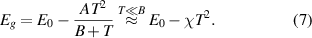
The latter approximation has been shown to describe well the temperature dependence of the optical bandgap in phase-change materials [136, 141]. The temperature dependence of the bandgap in crystalline semiconductors is usually associated with an increase of the interatomic spacing when the amplitude of the atomic vibrations increases with increased thermal energy, and temperature dependent electron-lattice interactions [140].
At low temperatures, it has been shown that the transport mode in some phase-change materials deviates from the trap-limited band transport to hopping transport, where the conduction comes from tunneling in localized states [135]. An approach to derive the conductivity by taking into account the state occupancy is presented in [142], and the hopping contribution to the conductivity is calculated by integrating over the whole set of occupied localized states i:
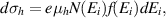
where µh is the hopping mobility, N(E) is the density of states and f(E) the Fermi occupation function. The hopping mobility can be calculated, at low-field conditions, from the Einstein relation [115]

The diffusion coefficient D is proportional to the square of the distance rij between the two hopping sites i and j, the jump probability νij from site i to j and the density of unoccupied states j [115, 142]
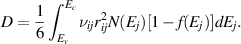
The complete formula for the hopping conductivity is then given by
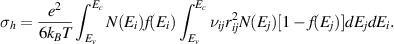
The main task is to then find proper expressions for rij and νij. We refer the reader to the literature for various expressions that have been proposed [142–144].
Typically, hopping mobilities are much lower than band mobilities. Therefore, the number of carriers in states around the Fermi level must be much higher than the number of carriers that are excited into the band, so that hopping transport can outweigh band transport. Hence, hopping transport will be important in materials with a large bandgap, high defect densities and at low temperatures. In common phase-change materials such as GeTe or Ge2Sb2Te5, it is believed that hopping transport takes over band transport at temperatures below approx. 200 K [135, 145, 146], where a single activated behavior cannot describe the low-field conductivity anymore.
4.1.2. Voltage dependence.
A recent review on the current state of knowledge related to subthreshhold conduction in amorphous phase-change materials, that is for applied voltages below the threshold switching voltage, is presented in [147]. Here, we will cover only the multiple-trapping case, that is when the transport occurs via extended states. This transport mode is expected to be valid at temperatures above approximately 200 K in common phase-change materials, and is thus relevant for technological applications where operation at room temperature and above is expected. For field-dependent conduction in hopping transport, we refer the reader to the literature [148–150]. Moreover, we focus only on the Poole–Frenkel effect, which has been the most commonly used mechanism to describe the field dependence of the conductivity in phase-change materials. A discussion on alternative transport mechanisms such as Schottky emission or space-change limited conduction based on experimental results can be found in [151].
To explain the variation of conductivity with the electric field in the multiple-trapping picture for disordered materials, the Poole–Frenkel effect is commonly used [152–154]. The Poole–Frenkel model is based on thermal emission from ionizable defect centers that are assumed to create a Coulomb potential. The ionization energy is then lowered upon the electric field by βF1/2 with  , where F is the applied electric field, e the electronic charge,
  0 the vacuum permittivity and r the relative high-frequency dielectric constant. The conductivity is expected to follow a law (Poole–Frenkel) of the form
When the defect centers are close to each other, so that there is significant overlap between the Coulomb potentials, it has been shown by using a two-center Coulomb potential that the ionization energy lowering upon field is eFs/2 [153]. The conductivity is then expected to follow a law (Poole) of the form
where s is the distance between the two centers. The prefactors  and
and  can have a weak field dependence
  where γ typically varies between −2 to 0. This field-dependence depends on the assumptions made on the mobility (whether it varies with the field or not) and whether spherical emission (3D) or emission only in the direction of the field (1D) is considered [153].
Most of the early work on field dependence of conductivity in phase-change materials focused on as-deposited thin films and Poole–Frenkel type transport was typically observed at high fields [137, 155]. One of the first studies of electrical transport in nanoscale PCM devices was by Ielmini and Zhang where they mostly observed an ohmic regime at low fields and Poole-type behavior at higher fields [106]. They proposed a reinterpretation of Hill's double-center Coulomb potential model [153] for phase-change materials, associating s to an intertrap distance Δz, considering that the double Coulomb potential profile is created by two neighboring donor traps. The electrons are assumed to be excited from the Fermi energy to the band edge and travel a fixed distance Δz in the band before being re-trapped. The currents flowing in and against the electric field direction are added and subtracted, respectively, leading to a sinh dependence of the current as a function of applied voltage.
However, experimental measurements since then clearly showed the existence of three distinct regimes, an ohmic regime, a Poole regime and a Poole–Frenkel regime [156, 157]. The ohmic regime occurs at very low fields and the transition from Poole to Poole–Frenkel conduction occurs at high fields [158]. Moreover, the point at which this transition occurs may vary upon structural relaxation [159]. In the past, this transition from Poole to Poole–Frenkel conduction had been investigated in the general context of disordered materials. In one approach, proposed by Ieda et al, a state of energy δ below the conduction band was introduced in which the electrons are considered as free carriers [154]. Recently, this approach was applied to phase-change materials by Beneventi et al [158]. The resulting derivation gives a simple analytical description of the conductivity in which the transition from Poole to Poole–Frenkel conduction can be tuned by adjusting the parameter δ. However, the physical origin of this state of energy δ below the conduction band remains rather unclear.
Yet another model by Pillonnet et al showed that the Poole to Poole–Frenkel transition could also be deduced from Hill's approach [153] by considering a carrier in a pair of Coulombic wells separated by a distance s [160]. It simply comes from the fact that the peak of the inter-center barrier is not at s/2 anymore at high electric field and the influence of the second center can be neglected. This leads to an energy barrier lowering of βF1/2 as for the single Coulomb potential. Here as well, just like the model of Ielmini and Zhang [106], immediate re-trapping after emission, which leads to a constant travel distance of the charge carriers, was assumed. Le Gallo et al extended this model to adhere to the original multiple-trapping picture, in which the conductivity is calculated based on the transport of carriers via extended states, without limiting the free travel distance to the nearest-neighbor distance [151]. The field dependence of the free carrier density was then captured via 3D Poole–Frenkel emission of carriers from a two-center Coulomb potential. This model was shown to capture experimental data both in as-deposited phase-change material thin films and nanoscale PCM devices over a wide range of temperatures and applied voltages [145, 151]. Subsequently, Kaes et al showed that s should depend on the occupation of the defect states. Thus, a temperature dependence of s arising from the Fermi occupation function is expected [145, 146]. Such a temperature dependence could successfully explain electrical I–V characteristics of different as-deposited phase-change materials both in the dark and under illumination using this model [145, 146]. Experimental measurements of the resistance versus applied voltage of a PCM device in the RESET state at different ambient temperatures along with a simulation using the model of [151] are shown in figure 14.

Figure 14. (a) Resistance of a PCM device in the RESET state as a function of voltage at different ambient temperatures. The device was RESET and annealed at room temperature for 1000 s prior to measurement. (b) Low-field resistance R of the device as a function of the temperature. R follows the Arrhenius-type behavior of equation (6). The simulations in (a) and (b) were done with the model presented in [151]. Reproduced from [151]. © IOP Publishing Ltd. CC BY 3.0.
Download figure:
Standard image High-resolution imageWe also point out that at very high electric fields and low temperatures, thermally assisted tunneling and direct tunneling through the barrier can occur, which will lead to a stronger field dependence of the conductivity than equations (8) and (9). The effect of tunneling in the Poole–Frenkel model was considered in the original work of Hill [153], and subsequently by Vincent et al [161], Martin et al [162] and more recently by Kaes et al [145]. Thermally-assisted tunneling denotes the combined process of excitation by a phonon and subsequent tunneling through the potential barrier. It leads to a field dependence of the conductivity of  where F2 depends on the temperature [161]. At higher fields, direct tunneling through the barrier becomes more probable than thermally-assisted tunneling, and the field-dependence of the conductivity follows the Fowler–Nordheim formula
  [161]. The total emission probability due to thermally-assisted tunneling and direct tunneling from a single defect can be written using the Wentzel-Kramers-Brillouin (WKB) approximation [162]. We note, however, that such models considering tunneling only from a single defect state cannot quantitatively reproduce the experimental I–V characteristics measured on line cells of as-deposited amorphous phase-change materials [145].
While the Poole–Frenkel model appears to describe well the electrical I–V characteristics of phase-change materials, the precise influence of different types of defect states on the transport properties under an applied field should be investigated further. Specifically, while (charged) deep defect states may create Coulomb potentials and would be responsible for Poole–Frenkel-type transport, the role of tail states remains unclear. This role would be especially relevant to assess because tail states are omnipresent in amorphous semiconductors as they simply arise from disorder. Deep defects, on the other hand, are usually related to specific bonding configurations and may thus not be present in all amorphous phase-change materials, especially with the correct charge state that would lead to the Poole–Frenkel effect. Therefore, models such as field-induced delocalization of tail states close to the mobility edge with increased electric field [147] may be relevant to derive and include for a more refined picture of electrical transport in amorphous phase-change materials.
Finally, with respect to device scaling, it would be expected that when the dimension of the amorphous region becomes comparable to the distance between the defect centers s, the Poole–Frenkel approach may not be appropriate anymore. Indeed, in such a case the amorphous region might contain only one (or no) defect state responsible for the Poole–Frenkel effect. Quantum transport approaches would likely be the most accurate tool to study the behavior of highly scaled devices [110]. Scattering effects should be carefully implemented in such simulations because the mean free path in amorphous semiconductors is comparable to the interatomic spacing due to the low mobility [115, 163]. Therefore, in contrast to crystalline semiconductors where ballistic transport usually occurs in highly scaled devices, in amorphous semiconductors diffusive (non-ballistic) transport might be expected even down to the smallest device dimensions.
4.2. Resistance drift
At constant ambient temperature, the low-field resistance of PCM typically exhibits a temporal dependence characterized by

where R(t0) is the resistance measured at time t0. The drift exponent νR, which typically has a value of 0.1 for the RESET state, exhibits significant inter-device and intra-device variability. Resistance drift is caused by the phase-change material in the amorphous phase. Hence, the drift exponent is lower for the SET state (< 0.05), in which the material is mostly in the crystalline phase, but rarely goes down to exactly 0 in melt-quenched PCM (see figure 13(b)). Drift variability across different resistance states and devices is arguably the most significant challenge for multi-level storage in PCM, because it ultimately limits the number of levels that can be stored and reliably retrieved in a memory cell [164]. Resistance drift can also have implications in non-von Neumann computing applications [37, 39]. First, we present a description of structural relaxation in phase-change materials, which is generally believed to be the root cause of resistance drift [165–167]. Next, we present modeling and characterization efforts to describe resistance drift in PCM devices.
4.2.1. Microscopic origin of resistance drift.
Resistance drift in PCM devices has been mostly explained as a consequence of spontaneous structural relaxation of the amorphous phase-change material [159, 165, 166, 168]. This structural relaxation is a direct consequence of the amorphization process described in section 3.2. When the molten phase-change material is quenched rapidly, the atomic configurations are frozen into a highly stressed glass state. Over time, the atomic configuration of this state will relax towards an energetically more favorable 'ideal glass' configuration. The observed increase in resistance has been shown to be a consequence of the atomic rearrangements resulting from this evolution [167, 169–171].
Recent first-principles calculations by Raty et al [167], Gabardi et al [170], and Zipoli et al [171] on the prototypical phase-change material GeTe provide significant insights into the microscopic picture of structural relaxation and the nature of the 'ideal glass'. Even more recently, the geometric and electronic structures of the localized states in the band gap of Ge2Sb2Te5 involved in the resistance drift process have also been analyzed [172]. In the crystalline phase of GeTe, both Ge and Te atoms are threefold coordinated. In [173], and later in more details in [171], it was found that most of the structures responsible for localized states in the band gap consist of groups of Ge atoms close to each other in which the coordination of at least one Ge atom differs from that of the crystalline phase. With some differences due to the criteria used to assign bonds, Gabardi et al [170] reported that drift results from the removal of chains of Ge-Ge homopolar bonds producing a widening of the band gap and a reduction of Urbach tails. Additional types of defects are made of four-fold tetrahedral coordinated Ge atoms and cubes not properly aligned. It has been shown that resistance drift is associated with a consumption of these defects towards lower-energy structures having chemical order and coordination numbers similar to that of the crystalline phase, and to a removal of stretched bonds in the amorphous network [171].
The role of stretched and compressed bonds is analyzed in figure 15 by plotting the correlation between conductivity and distribution of Ge-Te bond lengths. The histograms of normalized bond polarizations and bond distances show that an increase of resistance is linked to the topology of a-GeTe tending towards less stretched Ge-Te bonds with a distance of approximately 2.8 Å and bond polarization of 0.35. Structures with a higher number of these ordered bonds are less conductive.

Figure 15. Histograms of the bond polarizations of all the Ge-Te bonds versus the bond distance. Sixty-five structures, obtained via classical simulations and analyzed via first-principles calculations, are divided in five groups (GR) ranging from 1 (higher conductivity) to 5 (lower conductivity) and containing 14, 11, 17, 16, and 7 structures, respectively, see [171] for more details. The number of bonds in each bin normalized by the number of configurations of the group is indicated by the color scale. Configurations with a higher conductivity show a broader distribution. Upon relaxation, the Ge-Te bonds tend towards a sharper distribution of distances around 2.8 Å and bond polarizations of 0.35. Reprinted figure with permission from [171], Copyright (2016) by the American Physical Society.
Download figure:
Standard image High-resolution imageAlthough the studies done in [167, 170, 171] have some differences, they provide a rather clear picture of the processes involved during the relaxation towards the ideal glass. All those studies seem to agree that drift results in a consumption of defects in amorphous GeTe caused by groups of Ge atoms in which the coordination of at least one Ge atom differs from that of the crystalline phase. An increase in resistance is correlated with a consumption of these defects accompanied by a slow evolution of the bond network towards structures with chemical order and coordination numbers similar to those of the crystalline phase.
However, one difference in the conclusion of these works is whether the increase in resistance is related to a shift of the Fermi level towards mid-gap while the bandgap stays constant, or to an increase of the bandgap upon drift. Zipoli et al report that the bandgap stays rather constant upon moving from GR.1 to GR.5 (figure 15), but observe a lowering of the number of states in the bandgap which leads to a shift of the Fermi level towards mid-gap. This shift of the Fermi level increases the activation energy for conduction and thus results in an increased resistance [171]. In contrast, Raty et al report that bandgap widening occurs upon drift resulting from enhancement of the Peierls distortion linked to a reduction in the number of tetrahedrally coordinated Ge atoms [167]. Moreover, experimental observation of bandgap widening upon drift has also been reported via Fourier transform infrared spectroscopy (FTIR) measurements [174]. An in-depth comparison between the simulation methods used in the different works as well as the criteria used to define the bandgap will be required in order to understand the origin of this discrepancy.
4.2.2. Modeling and characterization of drift.
So far, most efforts have focused on modeling the kinetics of structural relaxation via a two-state model for the relaxation of defects [175, 176]. This is based on the popular relaxation model proposed by Gibbs [177]. The essential idea is that there are structural defects that can be removed by relaxation. Different activation energies are required to remove different defects assuming that the removal of one defect can be associated with a single activation energy. As the relaxation proceeds, defects with lower activation energies will be removed first, followed by those with higher activation energies. The distribution of activation energies for the relaxation of defects serves as the parameter that tracks the state of relaxation of the material at any instance in time.
Even though this model is quite appealing, it has a couple of drawbacks. In order to quantitatively capture the commonly measured log(t) drift behavior in phase-change materials, it is necessary to have a rather flat distribution of activation energies [175]. Since the log(t) kinetics have been observed over a wide range of time (from ∼100 ns [178] up to months) and temperature, the energy range over which the distribution is uniform would need to be quite large (presumably > 1 eV) [179]. Such a uniformly fine-tuned spectrum over a wide range of energy may not appear as the most physically plausible choice for relaxation in an amorphous material. Furthermore, in this picture, the defects that have undergone relaxation once no longer participate in subsequent structural relaxation processes.
An alternative modeling approach proposed recently is based on collective relaxation [169, 180, 181]. The essential idea is that the atomic configurations that are frozen in during the glass transition relax as a whole collectively towards the more energetically favorable 'ideal glass' state. The relaxation proceeds in a sequence of transitions between neighboring unrelaxed amorphous states. The driving force for such a relaxation is the difference between the local energy minima of two neighboring states. The closer to equilibrium the system is, the lower will be the driving force and the higher the energy barrier for subsequent relaxation. The key difference with respect to Gibbs approach is that relaxation is described with a single characteristic activation energy for relaxation that shifts in time, rather than a distribution of activation energies that gets eroded. This approach naturally gives rise to a logarithmic evolution of the relaxation without the need for unnatural requirements on the activation energy spectrum for the relaxation of defects. The main assumption required in this model to obtain the log(t) kinetics is that the activation energy for relaxation must increase linearly as the distance of the unrelaxed state from equilibrium decreases.
After establishing a model to describe the kinetics of structural relaxation, the relaxation needs to be linked to electrical observables such as the low-field resistance or more generally the I–V characteristics of a PCM device. In order to do so, most works have assumed that the change in device resistance upon drift is related to a change in the activation energy for conduction Ea (see equation (6)) [182–184]. This is consistent with the microscopic picture of structural relaxation presented in the previous section, because the activation energy is expected to increase upon drift from the consumption of mid-gap defects and bandgap widening due to local reordering [167, 170, 171, 174]. By equating equations (6) and (10), it is easy to show that Ea should take the form [182]

ED has been shown to be proportional to the temperature at which the device is annealed Tann [169, 182, 184], as expected from time-temperature superposition which should occur if the changes in Ea(t) indeed arise from structural relaxation [185]. Therefore, we can write  , which leads to equation (10) when resistance drift is measured at constant temperature T = Tann. The empirical dependence of Ea(t) described by equation (11) on both time and temperature has been experimentally proven by a wide range of works on PCM [169, 184, 186]. An additional dependency of the conductivity prefactor σ0 of equation (6) on time for some materials such as AIST has been reported [186], and its origin requires further investigations. Nonetheless, to describe the dependence of Ea on drift, one can link Ea with the parameter describing the state of relaxation of the material in a structural relaxation model. In the two-state relaxation model, this parameter is the number of unrelaxed structural defects [175], and in the collective structural relaxation model it is the distance of the unrelaxed state from the 'ideal glass' state [169]. With both approaches, a linear dependence of Ea on this parameter leads to a dependence similar to that of equation (11) for some finite range of time and temperature [169].
Experimental measurements of constant temperature low-field resistance drift over a wide range of temperatures are shown in figure 16(a). After setting the temperature to a certain value, the PCM device is RESET and the evolution of the low-field resistance R is monitored. It can be observed that the slope of log(R) versus log(t) is temperature independent in the experimentally accessible range of time [169, 182, 184]. However, when the ambient temperature is varied during the resistance measurement, reversible as well as irreversible effects of temperature on electrical transport occur upon drift, because structural relaxation is accelerated at higher temperatures [169, 180, 181]. An experiment showing the low-field resistance variation of a PCM device after RESET during the application of a time-varying temperature profile is presented in figure 16(b). When the temperature increases above room temperature, the relaxation is accelerated. Therefore, when the device is brought back to room temperature, its resistance becomes higher than if it would have stayed at room temperature for the entire duration of the experiment, and it stops increasing because of the preceding annealing at higher temperature.

Figure 16. (a) Low-field resistance drift of a PCM device in the RESET state at various ambient temperatures. (b) Low-field resistance drift of a PCM device in the RESET state (bottom) upon the application of a time-varying temperature profile (top). The simulations are performed with the collective relaxation model presented in [169]. Data from [169]. Reproduced from [169]. CC BY 4.0.
Download figure:
Standard image High-resolution imageThe dependencies of the resistance on time and temperature from experimental measurements reported in figure 16 can be equally well captured by both the collective relaxation model [169] (as shown in figure 16) and the two-state model for relaxation based on Gibbs approach [176]. With Gibbs approach, the activation energy spectrum for the relaxation of defects must be constructed to be sufficiently wide and flat (over > 1 eV range), such that the deviation from a log-law occurs in a range that is not experimentally accessible. As of now, it is not possible to discriminate between the two models from existing experimental resistance drift data. We hope that in the future molecular dynamics simulations will be able to provide reasonable estimates for activation energy spectra that will constrain the Gibbs model sufficiently to resolve this question. Other independent relaxation data not related to electrical transport, such as differential scanning calorimetry or shear modulus data as a function of relaxation [187], could also provide additional insights into the relaxation processes.
Besides the low-field resistance, many other observable parameters in PCM depend on structural relaxation. One widely reported observation is that the slope of log(I) versus V in the I–V characteristic increases with drift [169, 175]. This has been explained by an increase of the inter-center distance s in the Poole–Frenkel model with drift due to the annealing of defects [169, 175]. Another important parameter that changes upon drift is the threshold voltage, which has been shown to increase fairly linearly as a function of log(t) [101, 188]. The changes of the threshold voltage upon drift could also be explained by a change in the activation energy for conduction Ea, assuming that the threshold voltage is related roughly linearly to Ea [101, 188]. The viscosity has also been shown to increase with structural relaxation [189], which decreases the crystal growth velocity of the phase-change material [53, 64].
In addition to modeling and experimental characterization efforts, several approaches have been tried in order to counteract the effect of resistance drift to retrieve the stored information in a PCM device. One approach is to take advantage of the non-linearity of the I–V characteristic of the amorphous state (figure 13(a)) and obtain a better measure of the phase configuration, which is drift-invariant, by measuring the resistance in the high-field regime [190]. As seen in figure 13(a), the slope of log(I) versus V at high V can be used as a measure of the size of the amorphous region [151], and depends only weakly on drift compared to the low-field resistance. In the absence of a priori knowledge of the programmed state, the only way to explore the high-field regime of every programmed state is by applying a varying read voltage and then detecting the voltage or time at which a certain current threshold ( ) is reached. This voltage or time value (typically referred to as the M-metric) is used as the measure of the programmed state. It has been shown that the effect of drift can be significantly mitigated by using the M-metric [164, 190–192].
Another fascinating approach to eliminate the effect of resistance drift upon READ is building a so-called projected PCM device [193, 194]. This device comprises a carefully designed segment consisting of a non-insulating material (projection segment) that is parallel to the phase-change segment. The resistance of this projection segment is judiciously chosen such that it has only a marginal influence on the WRITE operation, but a significant influence on the READ operation. This is indeed possible because of the highly nonlinear nature of the electrical transport of the amorphous phase. The idea is that during WRITE the current flows through the phase-change segment because the resistance of the amorphous ON state is lower than the resistance of the projection segment. However, during READ, the current flows through the projection segment because it has a lower resistance than the amorphous OFF state. In this way, information retrieval is completely decoupled from information storage, and all the undesirable properties of the amorphous phase such as resistance drift, temperature dependence and noise are hidden upon READ. This approach has been shown to reduce the drift exponent by almost two orders of magnitude, and practically eliminate the READ current noise and temperature dependence [193]. A related approach is to built a PCM device with alternating stacks of phase-change and confinement nanolayers, which has been recently demonstrated to suppress noise and drift while retaining multi-level storage capability [195].
4.3. Noise
The most commonly observed type of noise in PCM is referred to as 1/f noise (or flicker noise), which is a type of noise frequently observed in electronic devices [196]. 1/f noise is characterized by a power spectral density inversely proportional to the frequency of the signal. 1/f noise in nanoscale PCM was first measured in [197], where the normalized current spectral density  of the amorphous state was reported to be two orders of magnitude higher than the crystalline state in GST. Later measurements showed that
  remains relatively constant with respect to the applied voltage for low enough voltages [198]. Experimental spectra of
  for crystalline and amorphous states measured in nanoscale GeTe line cells are shown in figure 17. A 1/f frequency dependence for the amorphous state is observed from 1 Hz to 100 kHz, and
  is roughly 105 times lower for the crystalline state. The ratio of
  between amorphous and crystalline states is usually observed to be comparable to the resistance ratio of the two states. Besides 1/f noise, random telegraph noise (RTN) is also typically observed in intermediate resistance states in PCM [199]. The current makes sharp transitions between two levels at random times and the fluctuation amplitude can sometimes be quite large, often resulting in a larger normalized variance than current signals of the RESET state.
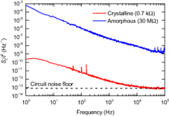
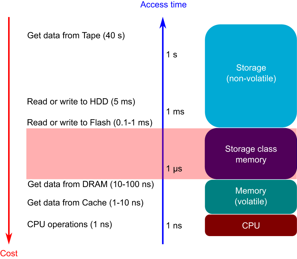
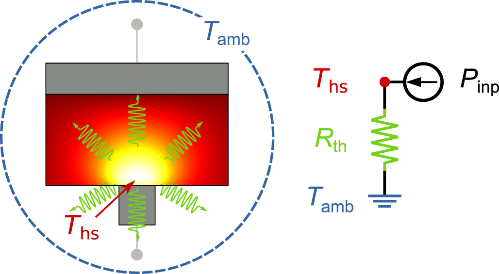
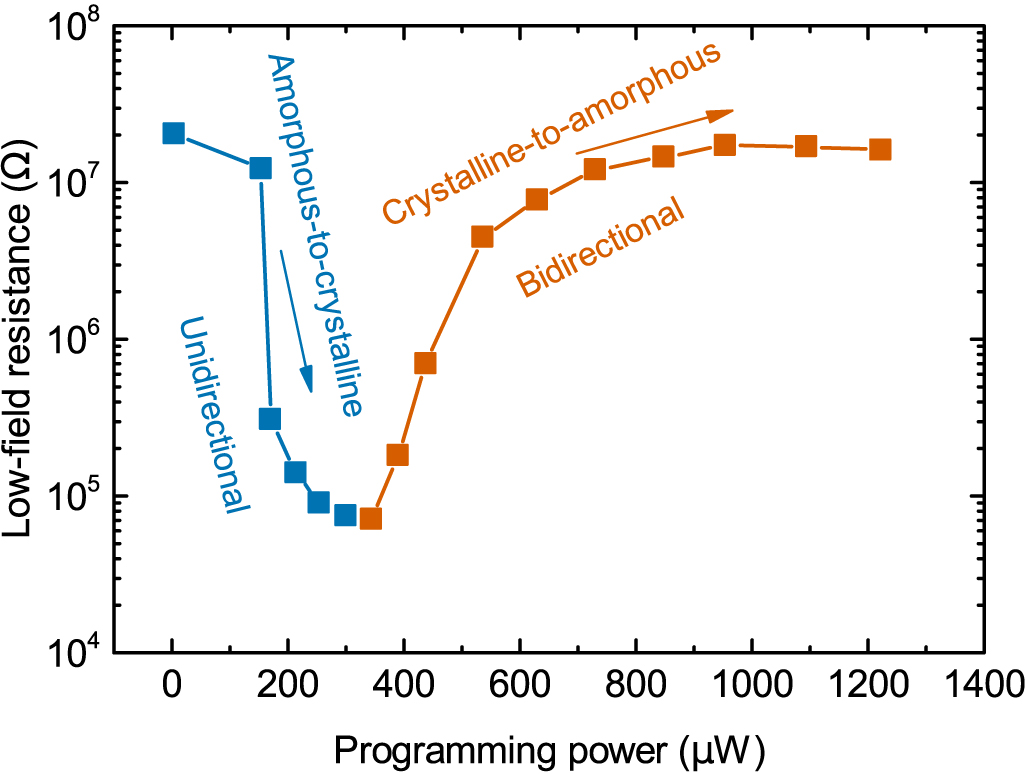
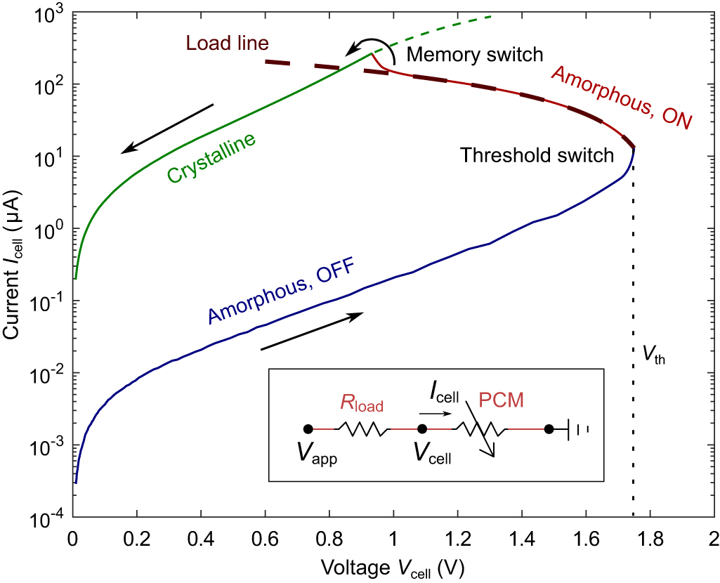
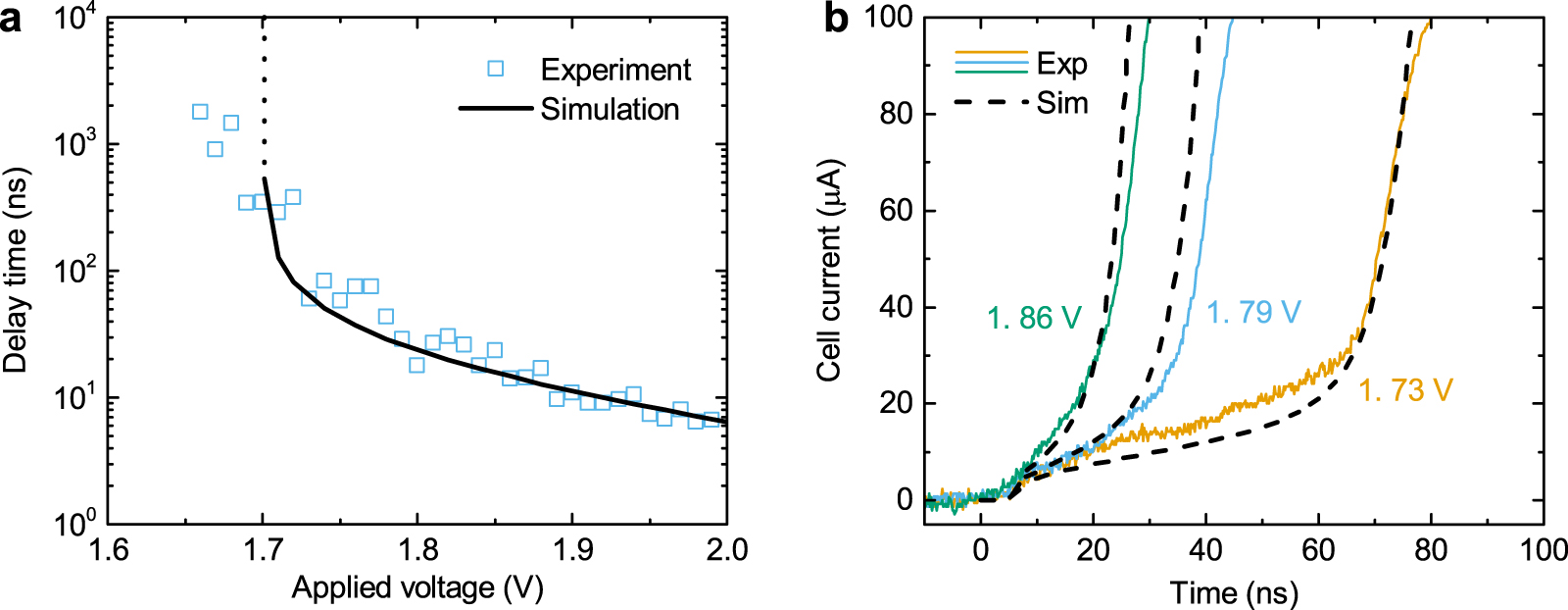
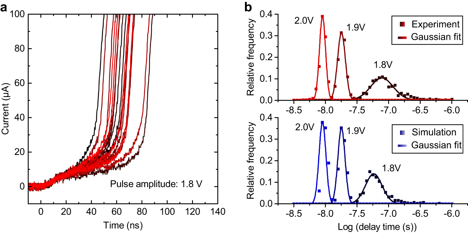
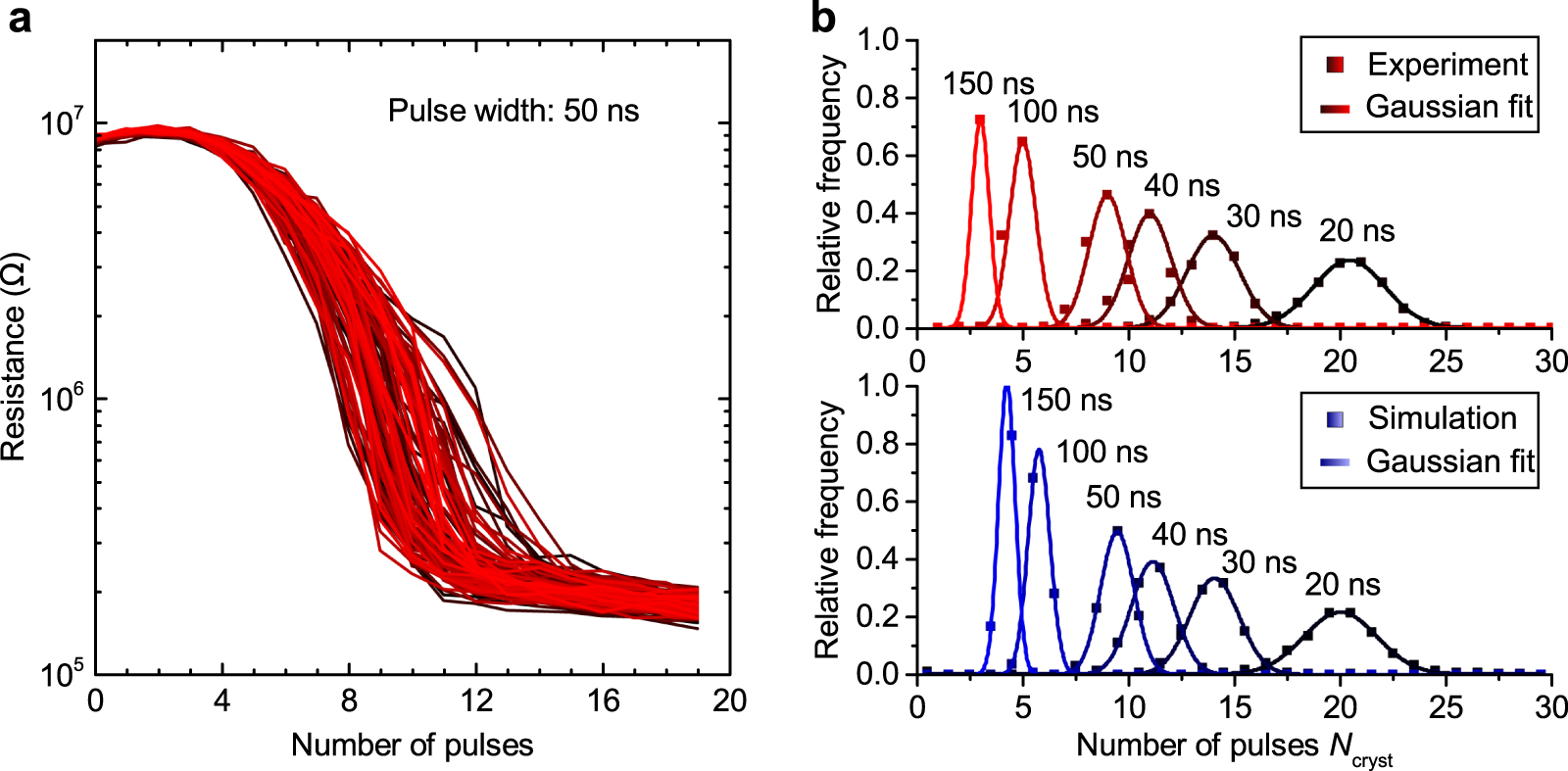
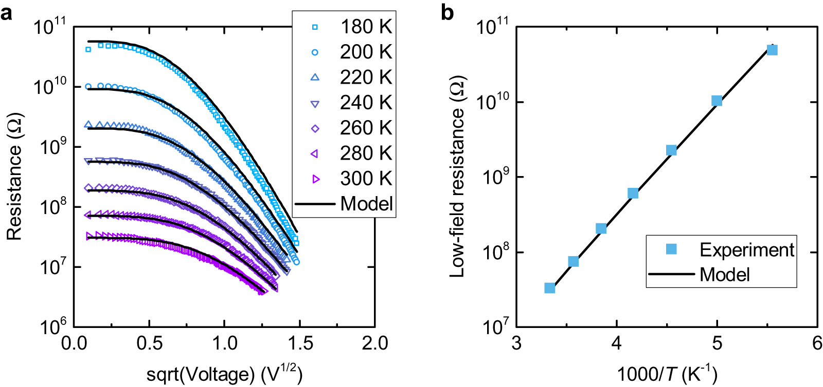
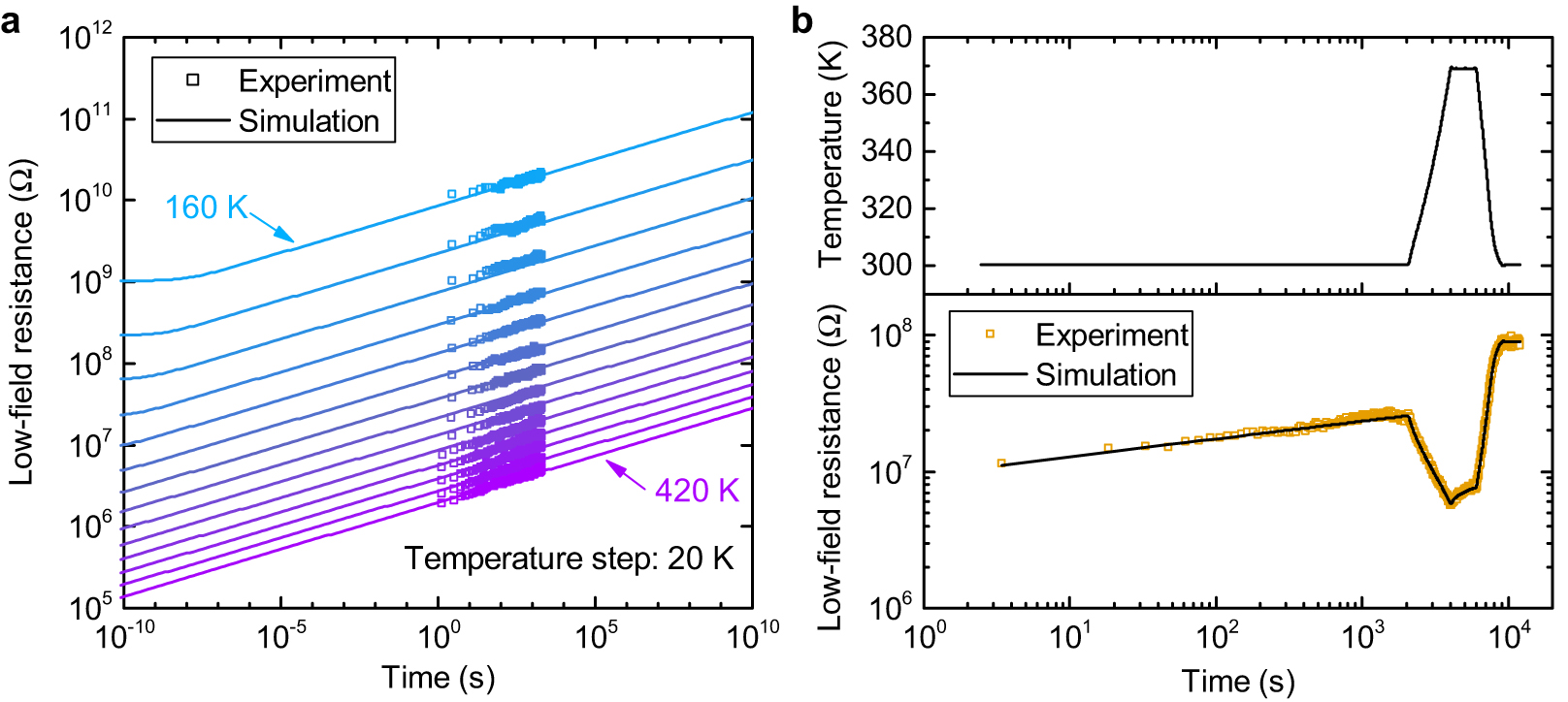
Figure 17. Normalized current spectral density  of amorphous and crystalline states in a nanoscale GeTe line cell. The applied voltage on the device is 59 mV. Adapted from [200].
Download figure:
Standard image High-resolution image
No unique model has been established for explaining the origin of 1/f noise in PCM. Few models have been proposed, mainly based on the concept of double well potentials (DWPs) [201, 202], in which either atoms or electrons switch between two energy minima separated by a potential barrier W, creating fluctuations. The general approach to arrive at a spectrum  is to assume that there are many fluctuation events, each with a relaxation time
  , where
  is the attempt frequency to surpass the barrier W. If it is then assumed that W is distributed uniformly, this approach yields a 1/f spectrum [201]. So in principle, any system which has local bistable configurations with an exponentially broad distribution of relaxation times would exhibit 1/f noise. The source of 1/f noise in the bulk electrical resistance can be related to charge carrier mobility or concentration fluctuations due to transitions in the DWPs [201]. In order to elucidate the precise underlying mechanisms in PCM, measurements of the temperature dependence of 1/f noise and its high-field non-Ohmic regime, in particular, would be required [201].
5. Outlook
PCM is arguably the most mature resistive memory technology as of today. The materials have been extensively studied and mass-produced, for example in DVDs and Blu-Ray disks, and it has already appeared as a digital memory product on the market (Intel Optane). Its attractive properties such as multi-level storage, fast read/write latency, non-volatility, good cycling endurance, and good scalability make it an ideal candidate for applications in novel computing paradigms. However, there are still several questions that remain to be answered regarding the crystallization mechanism, electrical transport, relaxation effects, and noise in PCM. Besides, there are also outstanding issues associated with the fabrication process of PCM for further scaling and integration with advanced CMOS technology nodes.
Although the crystallization mechanism in PCM devices has been successfully explained via crystal growth models [53, 64, 84], an exact determination of the glass transition temperature of the melt-quenched state in these devices is still lacking. This would lead to a better understanding of the state (glass or super-cooled liquid) in which the crystal growth mostly takes place at low temperatures (< 500 K). Moreover, the precise role of nucleation in PCM has not been studied as extensively as crystal growth. It might be important in neuromorphic computing applications, where low-power pulses are applied to incrementally crystallize the amorphous region. Indeed, for low-power pulses, the PCM temperature distribution might favor non-negligible nucleation in the center of the amorphous region. A better understanding of the role of material confinement and interfaces in the crystallization process is also very critical for ultra-scaled devices, for which the crystallization properties measured in as-deposited thin films of phase-change materials are unlikely to hold [203].
Regarding subthreshold electrical transport, the Poole–Frenkel model has been the most widely used to describe the variation of the conductivity with applied voltage in amorphous PCM. However, the precise influence of different types of defect states on transport remains unclear. Poole–Frenkel transport in PCM has generally been assumed to come from deep traps at a specific energy level with the correct charge state (e.g. acceptor-like defects for p-type transport) that form Coulomb potentials. Such defects have been detected via modulated photoconductivity in materials that contain germanium such as GeTe and GST [139, 204]. However, more recent measurements indicate a predominance of tail states rather than deep defects, especially in AIST [204]. Hence, a more realistic electrical transport model would need to account for trap and release processes of charge carriers with a continuous spectrum of localized states, rather than defects at a specific energy level [204]. Moreover, in ultra-scaled devices in which the size of the amorphous region becomes comparable to the inter-center distance in the Poole–Frenkel model, this approach is no longer valid and a different transport model would be needed as well.
There are also still many open questions regarding the threshold switching mechanism. Identifying a single mechanism that could quantitatively explain all features of threshold switching (static and dynamic) in all kinds of PCM devices and phase-change materials seems unlikely in view of the current literature. Although all the proposed thermal and electronic models so far can reproduce some experimentally observed characteristics of threshold switching, none of them appear to be able to quantitatively match all observed dependencies and dynamics over temperature and time across different materials and devices with realistic sets of physical parameters. Therefore, it appears reasonable to assume that threshold switching could be the combined result of many different mechanisms occurring at high fields, some of which would be more prominent in certain device geometries or materials. Further research in decoupling the thermal effects from the purely electronic ones in experiments is likely needed in order to better understand the role of each different mechanism in the final switching characteristics. One possible avenue could be to build devices with different thermal environments in order to vary the effective thermal resistance and capacitance, which should influence only the thermal processes leading to switching.
Regarding resistance drift, although its origin has been debated in the past [205], it is currently generally believed that it mostly arises from structural relaxation of the amorphous phase-change material. This interpretation has been supported by a wide range of experimental measurements and molecular dynamics simulations in recent years [167, 169–172, 175, 176]. Nonetheless, the changes in the electronic density of states resulting from structural relaxation are still being debated. Although it is generally accepted that the resistance increase is due to an increase of the activation energy for conduction, the origin of this increase (bandgap widening [167] or shift of the Fermi level due to annealing of mid-gap states [171]) needs further clarification. A better understanding of the quantitative link between the state of relaxation of the material, the density of defects in the bandgap and electrical observables would shed further light on the relaxation processes. Moreover, molecular dynamic simulations that could provide reasonable estimates of the activation energy spectra for the relaxation of defects would be helpful for discriminating between modeling approaches based on a distribution of activation energies [175, 176] or on a single activation energy dependent on the distance from equilibrium [169].
Lastly, noise has arguably been one of the least studied topics of PCM device physics, with only a few key works presenting experimental measurements [197–199, 206] and modeling approaches [201, 202]. However, noise poses very important challenges for both multi-level storage [207] and non-von Neumann computing with PCM [37, 39]. A much better understanding of the dependencies over temperature, voltage, and time, and of the physical mechanisms involved would be very helpful for directing the design of low-noise phase-change devices.
Besides the challenges related to the operational aspects of these devices, there still also remains significant issues associated with the fabrication process of PCM for successful integration in a computing system. In fabrication approaches that involve the deposition of phase-change materials in lithographically defined pore structures, achieving a dense, void-free, reliable phase-change material with the desired stoichiometry and resistivity post integration remains difficult [208]. In approaches that involve patterning of phase-change materials, the challenges involve maintaining the composition and surface morphology during the etch process [209]. For applications related to embedded memory and non-von Neumann computing, there are also challenges related to the back-end integration of PCM with advanced CMOS technology nodes. The relatively high programming current and threshold switching voltage pose significant challenges and limit the achievable areal density [33].
As PCM continues to mature and improve through the numerous efforts of researchers and industries, accurate physics-based models are expected to become more and more important. Such models could be included in a unified software package that would allow to accurately simulate PCM device and circuit designs for high capacity storage class memories and neuromorphic computing systems. Such accurate simulations would be of great help in directing the development of engineering solutions to address PCM non-idealities that could be implemented at a reasonable fabrication cost. Hence, there is definitely a demand for enhancing our understanding of PCM device physics, refining the already existing physics-based models of PCM, and potentially improving them based on more accurate physics, in order for PCM to be successfully integrated as memory and computing elements in next-generation computer systems.
Acknowledgments
We would like to thank our current and former colleagues at IBM Research–Zurich in particular, Evangelos Eleftheriou, Haris Pozidis, Daniel Krebs, Nikolaos Papandreou, Milos Stanisavljevic, Aravinthan Athmanathan, Angeliki Pantazi, Wabe Koelmans, Tomas Tuma, Federico Zipoli, Gael Close, Harish Bhaskaran, Prasad Jonnalagada, Urs Egger, Walter Haeberle, Martin Salinga, Matthias Kaes, Martin Ruetten, Benedikt Kersting, Iason Giannopoulos and Irem Boybat for their contributions. We would also like to thank our colleagues at the IBM TJ Watson Research Center, in particular Matthew BrightSky and Chung Lam as well as our academic collaborators. This work was supported in part by the European Research Council through the European Union's Horizon 2020 Research and Innovation Program under Grant 682675.