

Abstract
This paper introduces an on-chip acoustic graphene transistor based on lithium niobate thin film. The graphene transistor is embedded in a microelectromechanical systems (MEMS) acoustic wave device, and surface acoustic waves generated by the resonator induce a macroscopic current in the graphene due to the acousto-electric (AE) effect. The acoustic resonator and the graphene share the lithium niobate film, and a gate voltage is applied through the back side of the silicon substrate. The AE current induced by the Rayleigh and Sezawa modes was investigated, and the transistor outputs a larger current in the Rayleigh mode because of a larger coupling to velocity ratio. The output current increases linearly with the input radiofrequency power and can be effectively modulated by the gate voltage. The acoustic graphene transistor realized a five-fold enhancement in the output current at an optimum gate voltage, outperforming its counterpart with a DC input. The acoustic graphene transistor demonstrates a paradigm for more-than-Moore technology. By combining the benefits of MEMS and graphene circuits, it opens an avenue for various system-on-chip applications.
Export citation and abstract BibTeX RIS
1. Introduction
Recent advances in semiconductor industries require highly integrated and diversified microelectronic devices of small size, known as more-than-Moore technology. One of the embodiments of this stringent technology is to combine radiofrequency (RF) microelectromechanical systems (MEMS) devices with integrated circuits (ICs) on a single chip [1, 2]. By combining them monolithically, their functions can be expanded or improved by exploiting the merits of both components.
Resonators are typical RF MEMS devices, and play vital roles in frequency control and sensing applications [3–6]. Researchers have explored various methods to develop hybrid resonator–transistor devices. Vibrating body transistors or resonant body transistors share the silicon as both resonator body and transistor channel. The transistor is responsible for reading out the signal of the resonator, providing higher output-signal levels than capacitive transduction [7, 8]. Resonant high-electron mobility transistors take advantage of the piezoelectricity of gallium nitride (GaN) and its compatibility with a two-dimensional electron gas (2-DEG), enabling amplified detection of strain variation [9, 10]. Another promising approach utilizes the acousto-electric (AE) effect [11]. Resonators generate a series of acoustic waves which can transport the carriers in semiconductors. The transistor spares the DC voltage and shares the RF signal as the input power source [12–18]. These hybrid devices have proved to be effective tunable resonators [19, 20] and powerful tools for quantum studies [21, 22]. Of all the transistor channel materials, graphene has attracted growing research interest thanks to its superior properties. However, conventional acoustic wave devices using bulk lithium niobate (LiNbO3) or lithium tantalite (LiTaO3) crystals discourage effective gate tuning due to their large thickness. Top gate topology, which introduces a liquid dielectric material, succeeded in tuning the channel conductivity [23, 24] but was incompatible with the complementary metal oxide semiconductor (CMOS) process. Our previous work explored acoustic graphene transistors based on aluminum nitride (AlN) film [25]. Although the modulation is effective, such transistors have weak piezoelectric coupling and thus exhibit a tiny current.
To take advantage of the high coupling coefficient of LiNbO3 while also guaranteeing effective tuning of the graphene conductivity, we used LiNbO3 thin film on a silicon substrate. Acoustic wave devices based on LiNbO3 or LiTaO3 on a silicon substrate have been explored by numerous researchers [26–29], and recently surface acoustic wave (SAW) filters employing LiTaO3 thin film exhibited remarkable performance, marking a new era for acoustic resonators [30]. Encouraged by this idea, we fabricated an on-chip acoustic graphene transistor based on LiNbO3 thin film. LiNbO3 is used for both acoustic wave generation and the dielectric layer of the graphene transistor. A gate voltage can be directly applied to the silicon substrate and the 10 μm LiNbO3 thin film makes current modulation more effective than with the conventional bulk LiNbO3 substrate. Two acoustic wave modes, i.e. Rayleigh and Sezawa waves, carried the holes in graphene from the drain electrode to the source electrode, thus inducing a macroscopic current. The Rayleigh mode, with a higher coupling coefficient ( ), leads to a higher AE current. The input RF power and dependence of the gate voltage on the Rayleigh mode transistor were investigated and analyzed, and both proved effective at modulating the output current. With an input power of 24 dBm, the AE current can be enhanced by five times at an optimum gate voltage. Compared with typical transistors, the on–off ratio is greatly enhanced in acoustic transistors. The acoustic graphene transistor takes advantage of MEMS technology and graphene transistors, which is promising for development of integrated and multi-functional sensors and frequency components such as simultaneous detection of mass and electric charges and RF harvesters [31–35]. Our work demonstrates a paradigm of a hybrid MEMS and graphene device, taking a step forward in more-than-Moore technology.
2. Model and method
Figure 1 illustrates the acoustic graphene transistor. The resonator and the graphene field effect transistor (FET) share the LiNbO3 film: the resonator exploits it as a piezoelectric layer and the graphene transistor uses it as an insulating material. RF signals are applied to the interdigitated transducer (IDT) at port 1 and acoustic waves are excited in the LiNbO3 which can be detected by the other port. Acoustic waves propagate through the graphene and transfer momentum to carriers within it. As a result, the carriers move from the drain to the source and the transistor outputs a current. A gate voltage can be applied at the back side of the silicon to tune the conductivity of the graphene, thus modulating the output current. This back-side topology is a simple method for investigating graphene transistors and it is useful for proof-of-concept purposes [36].

Figure 1. Schematic illustration of the acoustic graphene transistor.
Download figure:
Standard image High-resolution imageWe used a finite element method (FEM) to simulate the acoustic wave device. Figure 2(a) illustrates the basic model of the resonator. To save computing time, we only built a cell with one wavelength. We used a piezoelectric devices model and frequency domain study. Periodic boundary conditions were applied to the two sides, and the bottom was fixed. A larger thickness of LiNbO3 contributes to a higher resonator quality factor, and the wavelength to thickness ratio is closely related to the coupling coefficient [37]. Given the fabrication capability, LiNbO3 is designed to be 10 μm thick and the pitch of the IDT is 6 μm, which corresponds to a wavelength of 12 μm.
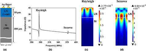
Figure 2. FEM simulation of the acoustic resonator. (a) Illustration of the resonator model. (b) Simulated frequency response of the resonator. The resonance peaks of the Rayleigh and Sezawa modes can be observed. The displacement profile of the Rayleigh (c) and Sezawa (d) modes (the unit of the displacement is meters).
Download figure:
Standard image High-resolution imageFigure 2(b) displays the simulated frequency response of the resonator. Frequencies ranging from DC to 400 MHz were swept and two modes were obtained, i.e. the Rayleigh mode and the Sezawa mode [38]. Figures 2(c) and (d) show the displacement patterns of the two modes. The false colors indicate the absolute displacement field. As the simulation results show, the maximum displacement in the Rayleigh mode is one order magnitude larger than that in the Sezawa mode. In the Rayleigh mode, most of the vibration resides in the piezoelectric layer, while in the Sezawa mode mechanical energy concentrates at the interface of LiNbO3 and silicon. As a result, the Rayleigh mode possesses a higher coupling coefficient, which is prone to induce a larger current in the graphene transistor.
Figure 3 illustrates the fabrication process of the device. First of all, X-cut LiNbO3 wafers and silicon (1 0 0) wafers were cleaned thoroughly and then directly bonded (figure 3(a)). After that, LiNbO3 was thinned to 10 μm (figure 3(b)). The thinning process included two steps: coarse mechanical grinding and fine polishing to the designed thickness (10 μm). Subsequently, 300 nm of gold was deposited on the LiNbO3 by physical vapor deposition (PVD) and was then patterned by lift-off, forming the IDTs, acoustic reflectors and drain and source electrodes (figure 3(c)). Monolayer graphene with poly(methyl methacrylate) (PMMA; purchased from ACS Material®) was transferred onto the center of the device, covering the drain and source electrode. The PMMA was removed by acetone, after which it was patterned by lithography and then etched by oxygen plasma (figure 3(d)). Finally, the device was cleaned in acetone.
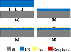
Figure 3. Illustration of the fabrication process. (a) Bonding of the LiNbO3 crystal and silicon substrate. (b) Thinning LiNbO3 to 10 μm. (c) Evaporation of gold and formation of the electrode pattern by lift-off. (d) Graphene transfer and pattern.
Download figure:
Standard image High-resolution image3. Results
Figure 4(a) displays an optical image of the acoustic device at port 1 and a scanning electron microscope (SEM) image in a zoomed-in view. The pitch of the IDT is 6 μm with a duty ratio of 0.5, corresponding to a wavelength (λ) of 12 μm. Each IDT is composed of 90 pairs of electrodes with an acoustic aperture of 60λ. Sixty shorted electrodes act as reflectors. The two IDTs have a center-to-center distance of 135λ. In this case, the fingers are parallel with the z-axis of LiNbO3 and the acoustic wave propagates along the y-axis. The drain and source electrodes are located at the center of the device, with an interval of 10 μm, as shown in figure 4(b). The SEM image shows the patterned graphene with a channel length of 10 μm and a width of 400 μm. Figure 4(c) shows a cross-sectional view of the acoustic wave device. As observed, 10 μm X-cut LiNbO3 was firmly bonded to the silicon substrate. Figure 4(d) displays the Raman spectrum of the graphene, which indicates its single-layer characteristics.

Figure 4. (a) Optical image (left) of the acoustic wave device at port 1. The SEM image on the right shows a zoomed-in view of the fingers. (b) Optical image (left) of the drain and source electrode of the transistor. The SEM image on the right shows the patterned graphene. (c) Cross-sectional view of the acoustic wave device, showing the profile of the Au fingers, the LiNbO3 film and the Si substrate. (d) Raman spectrum of the graphene.
Download figure:
Standard image High-resolution imageAfter a short-open-load-through calibration, a pair of ground-signal probes connected to a vector network analyzer (VNA) were used to interrogate the electrical performance of the acoustic wave device. Figures 5(a) and (b) show the transmission coefficient and reflection coefficient of the Rayleigh and Sezawa modes, respectively. For both modes, the impedance values from port 1 were extracted from S11, as presented in figures 5(c) and (d), respectively. Owning to a large acoustic aperture, there exists a transverse mode which degrades the electrical performance [39, 40]. The introduction of suppression methods, such as an apodized structure, is encouraged and will be addressed in our future work. The coupling coefficient of the two modes was calculated using equation (1),
where fs and fp are the series resonance frequency and the parallel resonance frequency, respectively. The Rayleigh and Sezawa modes exhibit coupling coefficient factors of 11.5% and 1.6%, respectively. Consistent with the simulation result, the Rayleigh mode presents a much higher coupling coefficient than the Sezawa mode.
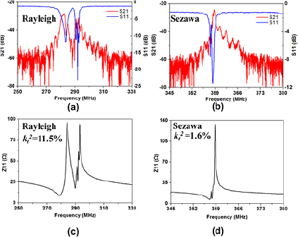
Figure 5. Measured electrical performance of the acoustic wave device. Transmission coefficient and reflection coefficient of the Rayleigh mode (a) and the Sezawa mode (b). Impedance value extracted from port 1 of the Rayleigh mode (c) and the Sezawa mode (d).
Download figure:
Standard image High-resolution imageWe evaluated a typical graphene transistor without acoustic waves. A semiconductor analyzer (Agilent B1500) was used to detect the drain–source current and to apply the gate voltage. Figure 6(a) shows the output characteristics of the graphene transistor with gate voltages of −30, −15, 0, 15 and 30 V, respectively. The curves demonstrate ohmic contact between the graphene and the electrode and prove effective modulation of the graphene conductivity through gate voltage. Figure 6(b) shows the transfer characteristics of the transistor. The gate voltage was swept from −30 to 30 V and the DC bias was 1 mV. The transistor shows p-type characteristics, which is typical for graphene exposed in an air environment [41].

Figure 6. Measured electrical performance of a typical graphene transistor without acoustic waves. (a) Output characteristics of the transistor, with gate voltages of −30, −15, 0, 15 and 30 V, respectively. (b) Transfer characteristics of the transistor under a DC bias of 1 mV.
Download figure:
Standard image High-resolution imageWe then measured the performance of the acoustic graphene transistor. The device was attached to a blank chip covered with gold by conductive silver epoxy; therefore a gate voltage could be conveniently applied to the chip surface (also the back side of the transistor). The transistor and chip were mounted together on a printed circuit board (PCB) and all the electrical pads were wire bonded to the PCB. A RF signal generator connected with a power amplifier (with a typical gain of 34 dB) offered a RF power through a co-axial SubMiniature Version A connector. The input powers mentioned below all refer to the amplified powers. A RF signal with an input power of 24 dBm was applied to the device. Without a DC bias, the frequency responses of the transistor induced by Rayleigh and Sezawa acoustic modes are recorded in figures 7(a) and (b), respectively. The positive current suggests that holes were transferred from drain to source. For both modes, the frequency response of the transistor follows the pattern of the transmission coefficient of the acoustic resonator in figures 5(a) and (b). The discrepancy arises from the sweeping intervals set in the VNA and the generator. Since the VNA supports a much finer frequency sweep, the current fails to closely follow S21 at each frequency. We focused on the peak value for both modes. For the Rayleigh mode, the maximum current reached 29 μA at around 287 MHz, while for the Sezawa mode, the current rose to 2.3 μA at 360 MHz. The Rayleigh mode results in a current that is an order of magnitude larger than that of the Sezawa mode, and this is mainly ascribed to its larger  , which is indicated by the relaxation model of the AE current [42].

Figure 7. Frequency response of the acoustic transistor, induced by the Rayleigh mode (a) and Sezawa mode (b), respectively. The length of the contacts used to measure the current is 10 μm.
Download figure:
Standard image High-resolution imageSince the Rayleigh mode provides a larger current, the subsequent study was focused on this mode. We investigated the power dependence on the AE current. An input power ranging from 14 to 24 dBm with a frequency of 286 MHz was applied to the device. Figure 8(a) shows the dynamic response for various input powers. The input power was turned on and off in turn, each for 40 s. It is obvious that a larger input power leads to a higher current. The current induced by different input powers is shown in figure 8(b). The power has a linear dependence on the AE current, which agrees well with the classic relaxation model.
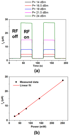
Figure 8. Dependence of RF power on the AE current. (a) Dynamic response of the current with various input powers. (b) Current as a function of input power.
Download figure:
Standard image High-resolution imageWe then studied the gate tuning of the acoustic transistor. The gate voltage was swept from −30 V to 30 V. RF signals with input powers of 14, 16.5, 19, 21.5 and 24 dBm were applied to the device in turn. Figure 9(a) shows the tuning result. For each input power the current decreases slightly with gate voltage under −15 V. The current increases rapidly when Vg is larger than −15 V and reaches a maximum value at Vg = 30 V. For a larger input power, the current increases at a larger scale. With an input power of 24 dBm, the current was escalated five times due to gate voltage tuning. Compared with the transistor without acoustic stimulation (see figure 6(b)), the effect of gate modulation was obviously increased in the acoustic transistor. With an optimum gate voltage, the AE current can be enhanced five times. We examined the gate tuning effect in the time domain. A RF signal with input power of 21.5 dBm was turned on and off in turn. Gate voltages of −30, −15, 0, 15 and 30 V, respectively, were applied to the back side of the device. In accord with figure 9(a), the current was a minimum for Vg = −15 V and a maximum for Vg = 30 V. Figure 9(c) describes the dependence of power on the AE current for various gate voltages. The current is linear with respect to the input power with each gate voltage. The slope of the curve is a maximum for a gate voltage of 30 V, demonstrating that the gate voltage can effectively tune the AE current.
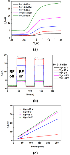
Figure 9. Gate tuning of the acoustic transistor. (a) Transfer characteristics of the acoustic transistor with various input powers. (b) Dynamic response of the AE current under different gate voltages. (c) Current as a function of input power with various gate voltages.
Download figure:
Standard image High-resolution image4. Discussion
To better understand the working mechanism of the acoustic transistor, we analyzed the data using the relaxation model [13, 23, 24]. The AE current density j can be described by
where μ is the hole mobility in graphene, Γ is the attenuation coefficient, I = P/Wdevice is the power intensity (Wdevice is 1.62 mm as indicated in section 3, P is the power injected to the SAW) and v is the velocity of Rayleigh mode (~3420 m s−1, extracted from figure 5(c)). μ is given by
where C is the capacitance of the graphene transistor, σ is the conductivity of the graphene and Vg is the gate voltage. The capacitance can be calculated by C = εxε0/dLN = 3.75 nF cm−2, where ε0 is the permittivity of free space, and εx and dLN are the permittivity and the thickness of the X-cut LiNbO3, respectively. σ can be obtained from the transfer characteristics of the DC transistor (figure 6(b)) by the equation σ = (Id/Vd) × (L/W), where L and W are the length (the separation between contacts, 10 μm) and width (400 μm) of the transistor channel, respectively [24]. We extracted μ from figure 6(b), and the value of μ ranges from 423 to 616 cm2 V−1 s−1, which is typical for graphene exposed in air.
Moreover, Γ is a function of the conductivity of graphene (σ)
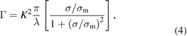
where K2 is the piezoelectric coupling coefficient, and σm is the material constant of LiNbO3. We use  of the Rayleigh mode obtained by equation (1) to represent K2. σm can be calculated according to the following equation:

where  and
and  are the dielectric constants of LiNbO3 at constant stress [18].
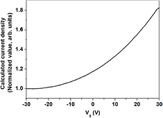
After extracting the values of Γ and μ, we can obtain the current density j according to equation (2). The calculated value was normalized by the minimum value obtained [23] and is plotted in figure 10. The calculated value increases with gate voltage, which is consistent with the experimental result shown in figure 9(a). In accord with Okuda et al [23] and Bandhu and Nash [24], our device, which is exposed to air, presents the same characteristics as those immersed in solution while working in the p-type zone. The calculated values fit well with the measured results with small input powers, but with larger input powers the acoustic transistor appears to have a larger on–off ratio. This may arise from the increased temperature caused by large powers, and the higher temperature contributes to a faster increase in AE current [18].
Figure 10. Calculated AE current density (normalized value) as a function of gate voltage.
Download figure:
Standard image High-resolution image
Unlike conventional transistors, acoustic graphene transistors leverage acoustic waves rather than an electric field to transport carriers. According to the relaxation model, μ and Γ play important roles as tuning knobs in the acoustic transistor. Theoretically, at the Dirac point of graphene, μ is zero and thus the current can be completely switched off. When σ is equal to σm, Γ is maximum and so is the current. This unique attribute of acoustic graphene transistors thus offers a large on–off ratio compared with conventional graphene transistors [24]. Our device only exhibits p-type characteristics of graphene due to the exposure to air, and thus the tuning ratio is limited. Our future work will focus on isolating the graphene from an air environment; therefore graphene can present bipolar properties and the tuning effect will be enhanced.
By combining equations (2) and (4), we conclude that the AE current relates to K2/λv. In this device, the wavelength being the same, the AE current arising from different modes is determined by the ratio of the coupling coefficient and the velocity. It describes why the AE current arising from the Rayleigh mode is an order of magnitude larger than that triggered by the Sezawa mode. Furthermore, compared with our previous work which employed AlN thin film [25], the AE current is increased by two orders of magnitude with the same input power.
5. Conclusions
In conclusion, we have demonstrated an on-chip acoustic graphene transistor using LiNbO3 thin film. Rayleigh and Sezawa waves are excited in the piezoelectric layer and induce currents in the graphene transistor due to the AE effect. The Rayleigh mode triggers a current an order of magnitude larger than that induced by the Sezawa mode, owning to its larger ratio of coupling coefficient to wave velocity. We focused on the Rayleigh mode in the subsequent study. The AE current is highly dependent on the input RF power and scales linearly with it. The gate voltage effectively tunes the conductivity of graphene and therefore the AE current can be conveniently modulated by it. By using LiNbO3 thin film, we have not only realized a tunable acoustic graphene transistor but also acoustic transistors offer larger on-off ratios than conventional devices.
Acknowledgments
This work was supported by the Natural Science Foundation of China (NSFC No. 51375341), the 111 Project under Grant No. B07014, and the National High Technology Research and Development Program of China (863 Program) under Grant No. 2015AA042603.