
Abstract
We present a fast room temperature terahertz detector based on graphene loaded plasmonic antenna arrays. The antenna elements, which are arranged in series and are shorted by graphene, are contacting source and drain metallic pads, thus providing both the optical resonant element and the electrodes. The distance between the antenna's arms of approximately 300 nm allows a strong field enhancement in the graphene region, when the incident radiation is resonant with the antennas. The current passing through the source and drain is dependent on the graphene's conductivity, which is modified by the power impinging onto the detector as well as from the biasing back-gate voltage. The incident radiation power is thus translated into a current modification, with the main detection mechanism being attributed to the bolometric effect. The device has been characterized and tested with two bound to continuum terahertz quantum cascade lasers emitting at a single frequency around 2 THz and 2.7 THz yielding a maximum responsivity of ~2 mA W−1.
Export citation and abstract BibTeX RIS

Original content from this work may be used under the terms of the Creative Commons Attribution 3.0 licence. Any further distribution of this work must maintain attribution to the author(s) and the title of the work, journal citation and DOI.
Introduction
Terahertz (THz) photonics represents a rapidly growing research area because of several applications in spectroscopy, communications and imaging. In particular, because of the unique characteristics of this frequency range, such as its non-ionizing nature and its extreme sensitivity to tissue water content, THz imaging holds great promise for diagnostics and non-destructive analysis of biological tissues. The importance of THz radiation in communications stems from the fact that it is a non-allocated frequency range, and the potential for high speed data transfer rates because of the high carrier frequency. Accordingly, the development of fast reconfigurable THz optoelectronic devices, such as modulators and detectors, operating at room temperature has attracted a great interest in the scientific community. The detection of THz radiation without using broadband time-domain spectroscopic systems, remains particularly elusive and is traditionally based on intrinsically slow (<100 Hz) devices such as pyroelectric detectors, Golay cells or cryogenic operating detectors, such as Si-bolometers. Alternatively, graphene and other bi-dimensional nanomaterials have been demonstrated to be valid alternative materials in several reviews [1–3] and research articles [4–13], where detection has been achieved through several distinct mechanisms, such as the photovoltaic, the photo-thermal effect and the bolometric effect [1, 2]. Various arrangements have been used in order to improve the intrinsically fast but poorly efficient responsivity of graphene photodetectors. One of the most common and efficient routes is the exploitation of plasmonic resonant elements, thus boosting the light concentration and interaction with graphene [6–8]. Recently we have demonstrated THz detection with an architecture based on interdigitated bow-tie antennas shorted by graphene regions [13] by using a quantum cascade laser (QCL) source. The bow-tie unit element had the two arms fabricated with metals having different work-functions, thus achieving an asymmetric graphene doping. The main detection mechanism was attributed to the photovoltaic effect. Here we exploit arrays of planar antennas fabricated in series, following an approach already exploited in the mid-infrared range [14] and a fabrication design which is reminiscent of what has been already reported for THz amplitude modulators [15, 16]. However, since the antennas are finally connected to the source and drain pads, they not only provide the plasmonic resonance capable of concentrating the light in the gap region, but they also act as electrodes, thus efficiently collecting all the photocurrent contributions arising from the illuminated graphene areas. According to [13], the detection mechanism is attributed to photoconduction, which implies an overall conductivity change of the graphene between the electrodes [2]. In this regards, our approach differs profoundly from the previous detector design [13] which was rather described as a photodetector, being based on p-n junctions. The main detection mechanism here has been ascribed to the bolometric effect, following the general definition of bolometric effect reported in [1] which includes the change in conductivity due to both a temperature related modification of the mobility, and a modification of the carriers contributing to the current, reminiscent of the photovoltaic effect. However, even though there are similarities with the photovoltaic effect, the operation of this device still requires a DC bias to be applied between the source and drain contacts. The device architecture presented in this manuscript has been conceived in order to increase the light-matter boosting offered by plasmonic resonant antennas by fabricating sub-micron gaps capable of providing higher E-field enhancement compared to the results presented in [13]. In the previous interdigitated scheme a further reduction of the gap between the electrodes, fabricated with two metals having different work functions, was hindered by the non-trivial alignment between successive steps in the fabrication process of mm-size areas. This approach, instead, simplifies the overall procedure also by transferring and defining graphene regions on top of the antennas thus allowing the realization of sub-micron size gap. Previously [13], the choice of leaving the graphene exposed was mainly driven by the need to preserve the graphene mobility, at the cost of having the charge neutrality point as high as ~120 V. Here we report on the efficient room temperature bolometric detection of THz QCLs by using an integrated plasmonic antenna/graphene architecture yielding a maximum responsivity of ~2 mA W−1 and operating with gate voltage biases <20 V.
Methods
Antenna arrays were fabricated onto a SiO2/Si substrate (300 nm/525 µm thick) via electron beam lithography, Ti/Au metal evaporation (10/65 nm) and lift off. Monolayer graphene, grown by chemical vapour deposition (CVD) [17, 18] was then transferred on top of the arrays and selectively etched in an Oxygen plasma chamber after a second step of electron beam lithography in order to define arrays of graphene squares. Each square has an area = 9 µm2 shorting the gap between the antennas' arms. A final conformal dielectric layer of 80 nm of Al2O3 was then deposited on top of the sample via atomic layer deposition (ALD) in stop-flow mode using H2O/TMA precursors, thus encapsulating the graphene [19, 20]. This last step is crucial in order to reduce the hysteresis [21] and bring the Dirac point to bias voltages lower than 100–120 V which was observed in previous strongly p-doped samples. The device is composed of four different independent array areas where the lengths L of the antennas' arms were 24.5, 23.5 and 22.5 µm for each array unit cell. The width of the arms was 2 µm and the gap between each antenna unit was nominally 0.5 µm. The last quarter of the device was left free of any metallic patterning and consisted of a continuous graphene region. The 3 antenna arrays have a unit cell which is repeated in M columns and N rows in order to cover the total active region area of 1 × 1.2 mm2. The pitch of the antenna arrays was kept fixed to 1.5 l between the rows. Finally, the sample was mounted onto an Au/ceramic chip carrier with conductive Ag paste and wire-bonded to allow full electrical characterization and photocurrent measurements. A sketch of the final device, together with a schematic of the equivalent circuit is shown in figure 1(a), while figure 1(b) presents the details of a single unit cell as acquired with a scanning electron microscope (SEM).

Figure 1. (a) Schematic of one array of the device and the basic electronic circuit. The antennas' arms are shorted by graphene areas and work as electrodes for the transport of the photocurrent generated Iph in each graphene square when a THz radiation is impinging with the correct polarization and frequency resonant to the antennas. Each array is composed of M columns and N rows. A 80 nm thick layer of Al2O3 (not shown here) is deposited on top of the active detector area. Each graphene element has a resistance RG and a contact resistance RS. The device is biased at a variable voltage towards gate VG and at a constant voltage VSD between source S and drain D, being the total photocurrent generated detected by a lock-in amplifier placed in series. (b) Details of the single unit cell taken with the SEM microscope. The graphene is clearly recognizable and it seems to have collapsed in the gap between the electrodes.
Download figure:
Standard image High-resolution imageResults
A first mandatory step consisted of the electrical characterization of the device. This task was accomplished by using two Keithley source/measure units (Model 2400). The first provided a constant current (<50 µA) to the source/drain contacts whilst the second one provided a variable bias to the back-gate contact. The maximal resistance between source and drain RSD has been identified with the Dirac point. The results of the electrical characterization on this sample are reported in figure 2 together with the characterization of a similar device which has exposed graphene in the whole array area of 1 × 1.2 mm2. This non-encapsulated sample, as shown in figure 2(a), exhibited a Dirac point above 120 V, consistent with exposed strongly p-doped CVD grown graphene and in agreement with what has been already reported in [15, 16]. The array with L = 23.5 µm was shorted towards the gate. The use of ALD deposition in stop-flow mode results in a continuous Al2O3 layer that provides encapsulation and brings the Dirac point to lower voltages, as shown in figure 2(b). Figure 2(c) shows the source-drain resistance RSD of the area with a uniform graphene layer; the Dirac point was found at ~−60 V, consistent with n-doped graphene.
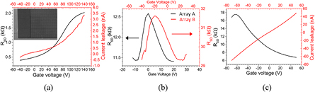
Figure 2. (a) Electrical characterization of antenna arrays with graphene exposed and continuously covering the whole area. (b) Electrical characterization of the arrays A and B where the graphene is only transferred in the antennas' gaps and the whole active area is encapsulated by the Al2O3 layer. The Dirac points were reduced from >120 V in (a) to <−20 V in (b). (c) Source-drain resistance RSD for a uniform graphene area is encapsulated by the Al2O3 layer.
Download figure:
Standard image High-resolution imageThe two arrays A and B, corresponding to antenna arm length L of 24.5 and 22.5 µm, respectively, have a Dirac point around 0 V and −20 V. We attributed this change of the charge neutrality point with respect to the uniform graphene area shown in figure 2(c) to metal p-doping provided by the Au contacts [22, 23]. The absolute value of the RSD in figure 2(b) is mainly determined by the contact resistance between the graphene areas and the antennas in each unit cell, differently from [13]. In that case, the graphene was covering uniformly the detector area and the antenna array was fabricated on top of the previously transferred graphene sheet, yielding a reduced contact resistance. In the present case, instead, it was preferred to transfer the graphene after the realization of the antennas, which was ultimately driven by the fabrication techniques required to resolve the <500 nm gaps between the antennas without damaging the graphene areas over the ~mm2 size arrays. Since graphene is shorting only the antennas and it is not filling the whole area it can be safely concluded that the current is flowing only through the gaps. Both samples in figure 2(b) have a finite leakage toward the gates (<100 nA) which prevented the acquisition of data for a wider range of gate voltages and a more detailed electrical characterization. The total resistance between source and drain RSD can be related to the sum of the resistance of a single graphene area RG and the metal surface contact resistance of each element RS by a multiplicative factor M/N, which corresponds to 40/34 for array A and 44/37 for array B. The capacitance between the antenna gap has been neglected since it has a high impedance and it is in parallel with the graphene element resistance.
The simulation of the plasmonic resonances and the optical design of the antennas has been performed with the commercial software Comsol Multiphysics v 5.1 based on finite element method in order to monitor the transmission and reflection of the final device using the |S21|2 and |S11|2 parameters of an incident plane wave with the polarization along the major axis of the antenna. The simulation window is based on a single unit cell with periodic boundary conditions in the plane of the antennas. A Drude model was implemented to simulate the optical properties of Ti/Au [24] and graphene through the complex permittivity [25]. The main plasmonic resonances of the antenna arrays A and B are shown in figure 3 for a graphene conductivity value of 0.3 mS, consistent with the RDS values reported in figure 2(c). The main resonances for array A and B are at 2.25 THz and 2.45 THz, respectively, which present a good overlap with the frequencies of the two QCLs used in this study; two single plasmon bound to continuum QCLs [26] emitting around 2 THz and around 2.7 THz, both in single frequency operation. This is a crucial requirement since mode hopping, multiple emission frequency and power fluctuations among different lasing modes would be difficult to deconvolve from the overall photocurrent response.
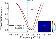
Figure 3. Finite element method simulated transmission for the antenna unit cells corresponding to array A and B for a graphene conductivity value of 0.3 ms. The broad resonant features, centered at ~2.25 THz and at ~2. 45 THz, respectively, have a significant overlap with the two QCLs used in this study, emitting in single frequency around 2 THz and 2.7 THz. The inset shows the normalized electric field at resonance for sample A.
Download figure:
Standard image High-resolution imageThe inset in figure 3 reports the normalized E-field at the resonant frequency for the first array: the electric field is almost completely confined in the gap, as expected. In order to confirm the simulations, the transmission of a sample similar to array A was tested with a THz time domain spectroscopic system, model TERA K15 from Menlo systems, yielding a broadband THz frequency response of the device. The whole apparatus was placed in a N2 purged environment to improve the signal/noise and increases the total bandwidth. The temporal waveform has been opportunely truncated in order to avoid multiple reflections, Fourier transformed and normalized to the background. The transmission has been acquired for both polarization parallel and perpendicular to the main axis of the antenna array. The results are shown in figure 4. When the polarization is parallel to the main axis of the antenna it is possible to clearly observe a resonant dip around 2.2 THz which is in very good agreement with the simulation showed in figure 3. Conversely, by changing the polarization by 90°, (rotating the sample) the resonance disappeared.
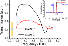
Figure 4. Measured broadband frequency response of a sample identical to array A for polarization parallel (black line) and perpendicular (red line) to the main axis of the antennas. A transmission dip is observed when the polarization excites the main plasmonic resonance of the antennas. The inset reports the time-domain waveforms for both parallel (black line) and perpendicular (red line) polarization, together with the reference signal acquired without the sample in the spectrometer's path (blue line).
Download figure:
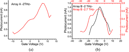
Standard image High-resolution imageWe implemented two powerful frequency stable QCL sources in an experimental setup schematically reported in figure 1(a), which is similar to the apparatus shown in [13]. The QCL emitting at 2 THz was operated in pulsed mode with a repetition rate of 2 kHz and 30% duty cycle at 5 K, while the second one was operated at a duty cycle of 10% and a repetition rate of 10 kHz at 5 K. The THz radiation was collimated with a 2'' effective focal length parabolic mirror and focused by a 1'' parabolic mirror on to the detector area. The powers emitted by the two lasers were calibrated by using a Golay cell placed after a 1 mm pinhole adjusted in the focus of the final parabolic mirror. A uniform power distribution over the illuminated area was assumed and the peak powers impinging onto the arrays have been estimated to be 0.11 mW and 0.16 mW, respectively. The graphene detector was placed in the focus of the optical system and was biased at a constant voltage between source and drain while sweeping the gate voltage. A lock-in (model 7265 from Signal Recovery) was placed in series with the detector using the QCL repetition rate as reference. When the radiation is impinging onto the detector a signal on the order of ~1 nA is detected. Conversely, no photocurrent was measured from the sample shown in figure 2(a) because the antenna electrodes were not contacting the main source and drain pads. The photocurrents measured at different gate voltages for array A at 2 THz and for array B at 2 and 2.7 THz are reported in figures 5(a) and (b) respectively, showing similar values and peaking at the corresponding Dirac points. The photocurrent measurements acquired with the two QC lasers seem to follow the same trend with different frequencies, as shown in figure 5(b), in good agreement with the electrical characterization reported in figure 2(b).
Figure 5. (a) Measured photocurrent for array A at 2 THz, and (b) for array B at 2 and 2.7 THz for different back-gate voltages. The measurements seem to follow a trend analogous to the corresponding electrical characterization shown in figure 2(b).
Download figure:
Standard image High-resolution image
A photocurrent analysis was performed following the model reported in [14] to better describe the physical mechanisms underlying the detection process. The total photocurrent output IL is given by IL = N · Iph · RG/(RG + RS + RL) where RL is the resistance in series given by the lock-in amplifier, 250 Ω, and Iph the photocurrent generated by a single unit cell. Since it is impossible to extrapolate from the RSD measurements of figure 2(b), the resistance of graphene in the single unit cell RG, this task was accomplished by attributing the same conductivity value of the sample shown in figure 2(c) to the graphene areas but shifted at the corresponding Dirac point. The photocurrent Iph in the graphene area is arising from the response of the photogenerated electron–hole carriers under a bias across the gap and it is given by equation (1):
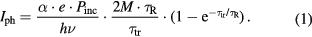
The power incident on the graphene area is Pinc, α is the absorption of graphene, which was assumed to be constant at 10% independently from the gate bias [13, 14], hν is the incident photon energy, e the electron charge, τtr is the carrier transit time and τR the carrier recombination time. The absorption at these frequencies is mainly determined by Drude mechanism due to intraband free carriers absorption [27]. The factor M is the hot carrier multiplication factor which scales linearly with the ratio between the photon energy and the Fermi energy ~hν/2EFermi [28] and represents the number of hot electrons created by one absorbed photon. M has been assumed to have its minimal value of 1. This crude estimation is justified by the fact that the photon energy is ~8 meV while the EFermi estimated at a voltage distance of ~10 V from the Dirac point is ~100 meV. The Fermi energy  was estimated by using the conventional formula already used in [25]
  where
where  is the reduced Planck constant, carea is capacitance per unit area per charge of SiO2 (7.4 · 1014 m−2 V−1), vF is the Fermi velocity (106 m/s) and ΔV is the voltage distance from corresponding Dirac point. Practically, the contribution of secondary hot electrons is neglected and it is assumed that the photocurrent is mainly determined by the photon absorption. The carrier transit time τtr is given by
  where g is the gap size, Egap is the electric field in the graphene channel and μ is the mobility that was assumed to be ~600 cm2 V−1 s−1 [20]. The values obtained for the carrier transit time τtr for Array A and B are 4.1 ps and 0.25 ps, respectively. The model implemented cannot retrieve the peaking of the photocurrent at the Dirac point. At the Dirac point the terahertz absorption due to the free carriers is minimal but the optical resonance has its maximum. The Fermi energy at the Dirac point is then comparable to the photon energy and the hot carrier multiplication factor M might be no longer unity. Due to the aforementioned effects, which have different trends and weights, it is difficult to develop the model further with the present data sets. It was preferred to calculate the photocurrent based on equation (1) for different recombination time constant τR. by using the model of equation (1). The recombination time constants for array A and B which could best reproduce the photocurrent measurements acquired at 2 THz and presented in figure 5 are τR ~ 0.26 ± 0.1 ps and 0.6 ± 0.3 ps, respectively.
Discussion
The recombination time constants retrieved by the model are in excellent agreement with the value obtained in [13] of ~0.22 ps and reported elsewhere in [4, 29, 30]. The responsivity which was calculated as the maximal photocurrent measured over the total power incident onto the graphene area is reported in table 1 for both arrays and both frequencies.
Table 1. Calculated responsivity for both arrays for different QCL frequencies.
| Responsivity (mA W−1) | QCL 1 (2 THz) | QCL 2 (2.7 THz) |
|---|---|---|
| Array A | 1.8 | 0.1 |
| Array B | 2 | 0.3 |
The maximum responsivity recorded was ~2 mA W−1 for array B at 2 THz which reduced to 0.3 mA W−1 at 2.7 THz. This is one order of magnitude higher than what has been previously reported in [4] for a graphene bolometer detector. The higher performance of array B compared to array A is attributed to random differences between the two samples during the several fabrication steps as well as to the higher leakage towards gate observed in array A. The ratio between the responsivities of the two samples suggests a trend which can be well described by the simulations presented in figure 3. Both arrays have higher responsivity at 2 THz because of their resonant frequency which seems to be closer to 2 THz. However, the second array which is blue-shifted in frequency compared to the first one, showed significant photocurrent also at 2.7 THz. Conversely, the responsivity of the first array is strongly reduced at 2.7 THz because of the poor frequency overlap with the plasmonic resonance. The maximum responsivity values achieved are ~30 times higher than what was reported in [13] and mostly achieved at significant lower bias voltages.
Conclusion
In conclusion, we have presented a photodetector operating at room temperature in the THz frequency range based on arrays of antennas shunted by graphene squares. The photodetection mechanism is attributed to the bolometric effect. The antenna's arms provide both the plasmonic resonance as well as the electrodes necessary for the charge extraction and transport. The Dirac points in these samples have been observed at voltages close to 0 V, thanks to the encapsulation of graphene in a Al2O3 layer deposited by ALD. The responsivity has been tested with two QCLs emitting in single frequency around 2 THz and 2.7 THz yielding results commensurate to the photocurrent model adopted and consistent with the finite element method simulations. The maximum responsivity has been increased to the record value of ~2 mA W−1 which together with the low voltages required to operate the device represents a great progress compared to our previous results and in the field of graphene-based integrated room temperature THz detectors in general.
Acknowledgments
RD, HEB and DAR acknowledge financial support from the Engineering and Physical Sciences Research Council (Grant No. EP/J017671/1, Coherent Terahertz Systems). SH acknowledges funding from EPSRC (Grant No. EP/K016636/1, GRAPHTED). KN acknowledges the University of Cambridge Nanoscience Doctoral Training Centre (EPSRC EP/G037221/1) for financial support.
Additional data
Additional data sets related to this publication are available from the Cambridge University data repository at https://doi.org/10.17863/CAM.8100.