

Abstract
Heat extraction is often essential in ensuring efficient performance of semiconductor devices and requires minimising the thermal resistance between the functional semiconductor layers and any heat sink. This paper reports the epitaxial growth of N-polar GaN films on polycrystalline diamond substrates of high thermal conductivity with metal-organic vapor phase epitaxy, by using a SixC layer formed during deposition of polycrystalline diamond on a silicon substrate. The SixC layer acts to provide the necessary structure ordering information for the formation of a single crystal GaN film at the wafer scale. It is shown that a three-dimensional island (3D) growth process removes hexagonal defects that are induced by the non-single crystal nature of the SixC layer. It is also shown that intensive 3D growth and the introduction of a convex curvature of the substrate can be deployed to reduce tensile stress in the GaN epitaxy to enable the growth of a crack-free layer up to a thickness of 1.1µm. The twist and tilt can be as low as 0.65° and 0.39° respectively, values broadly comparable with GaN grown on Si substrates with a similar structure.
Export citation and abstract BibTeX RIS
1. Introduction
There is a long term technical need for close contact between an electronic device and a low-cost substrate of high thermal conductivity for the efficient heat extraction that would improve performance stability and device lifetime. Polycrystalline diamond (PD) offers a combination of relatively low cost and high thermal conductivity (~2000 W m−1 K−1) but its surface does not provide sufficient atomic periodicity at the wafer scale for epitaxial growth. Recently it was demonstrated by Adikimenakis et al, using molecular beam epitaxy, that GaN layers could be grown on PD substrates. However, tilt in the grown films, determined from GaN(0 0 0 2) rocking curves, was as high as 2° [1]. Such a high degree of residual crystal disorder is not suitable for many device applications, for example, in GaN-based RF and power electronics, with the consequence that technology options developed to date involve the use of an intermediate layer between an electronic device and a PD carrier, such as a bonding layer [2], a Si(1 1 1) layer that offers a surface structure for epitaxy [3] or a SixN layer that is deposited on to the back of an electronic device to act as a seed layer for the growth of PD [4]. These approaches all suffer from the disadvantage that an intermediate layer of relatively low thermal conductivity is incorporated into the structure to introduce a barrier to heat conduction, and involve yield and performance limiting substrate removal processes [2, 4].
This paper reports that high-quality GaN epitaxy can be grown by metal-organic vapor phase epitaxy (MOVPE) on PD using a SixC layer associated with the growth of PD on a silicon substrate. This SixC layer is widely observed on the Si surface when the growth of PD is initiated [5, 6]. Further, the large difference in the coefficients of thermal expansion (CTE) of diamond [7] and GaN [8] will introduce high tensile stress in the latter after cool-down from the epitaxial growth temperature. To counteract this, we also demonstrate a growth technique that limits the effect of the non-single crystalline nature of this SixC layer on the GaN surface morphology and a novel approach for reducing the tensile stress in the GaN layer. As such, this work provides a route for the growth of GaN based devices on low-cost, heat-extracting PD substrates.
2. Experimental
Two kinds of PD substrate (hereafter called PDA and PDB) from different suppliers (Element Six Ltd, Diamond Materials GmbH) were used in the work, both supplied with their initial Si(1 1 1) growth substrate intact. In each case, the Si(1 1 1) was removed by immersion in hot KOH and/or an isotropic Si etching solution (a mixture of HNO3 and HF). A distinguishing feature of the two types of substrate after removal of the Si(1 1 1) substrate is their curvature, as shown in figure 1(a). The curvature measured by a stylus technique (Dektak Stylus profiler), shown in figure 1(b), occurs as a result of residual stress in the PD layers [9]. PDA substrates exhibited a convex bow (~1.5 µm over 5 mm) while PDB substrates had concave bow (~6 µm over 5 mm).

Figure 1. (a) Schematic illustration of PD layer growth on a Si(1 1 1) wafer with the SixC interlayer, the direction of bow of PDA and PDB substrates after removal of the Si(1 1 1) in the proposed III-nitride growth procedure. (b) Measured bow of both kinds of PD substrates. PDA has a convex bow (~1.5 µm over 5 mm) whilst PDB has a concave bow (~6 µm over 5 mm).
Download figure:
Standard image High-resolution imageX-ray photoelectron spectroscopy (XPS) and energy dispersive x-ray spectroscopy (EDX) were performed on the surface of each PD substrate to analyse their chemical nature. Figure 2 shows the XPS spectrum of one of the PD substrates used. It contains the signatures of Si–C and Si–O bonds to confirm that a SiC or SixC layer had formed during the PD growth and had survived the removal of the Si(1 1 1) by wet etching. However, the signature of the Si–Si 2p peak bond at ∼99 eV was not resolved, indicating that the wet etching procedure had successfully removed the elemental Si from the PD films. The Si–O bonds are formed in air and the oxygen is readily desorbed by annealing the PD substrates in H2 prior to MOVPE growth.
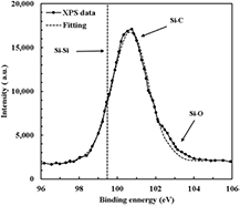
Figure 2. XPS spectrum measured from a PD substrate surface, which shows a well-defined Si–C 2p peak with a trace of silicon surface oxidisation.
Download figure:
Standard image High-resolution imageSince the combination of wet etches (hot KOH, HNO3 and HF) used will remove elemental crystalline Si, SiO2 and amorphous SiC, but not crystalline SiC [10], it is concluded that the SixC residue after etching is crystalline in character, but not single crystal due to its likely heterogeneous nucleation during or as a precursor to PD growth on Si [5, 6, 11]. A TEM study of cross sections of very similar PD-on-Si(1 1 1) structures confirm the presence of a few monolayers of SiC or SixC interlayer in a nano- or microcrystalline form [12].
III-nitride layers were grown on PDA and PDB in an AIX200/4HT-S MOVPE system after first growing an AlN or Al0.75Ga0.25N nucleation layer (figure 1(a)). As will be seen, the growth conditions and therefore structure of the nucleation layer play a critical role in the properties of the subsequently-grown GaN layer. Prior to any III-nitride growth, the PD substrate temperature was raised to ~960 °C, maintained at this temperature for 3–4 min to conduct a thermal cleaning process, and was finally decreased to ~800 °C for the AlN or (AlGaN) (10–40 nm) growth. The other growth conditions for the nucleation layers are: Pressure: 100 mbar; NH3 flow: 650 standard litres/minute (SLM); Trimethylaluminium (TMAl): 23 SLM; H2 carrying gas: ~4.5 SLM; and trimethylgallium (TMGa): 1SLM for AlGaN.
The GaN deposition was by a two-step process which comprises of a 3-dimensional island (3D) growth at a temperature below 1000 °C with a low NH3 flow (<850 SLM) and a 2-dimensional island (2D) growth at 1050 °C with a NH3 flow of 2000 SLM to promote lateral growth to form a continuous epitaxial layer, The duration of the lower temperature 3D growth process ranged between 7 min and 30 min in order to study the effect of its duration on the surface morphology.
For all samples, surface reflections were recorded during the growth of all samples using a LAYTEC EpiSense system [13]. Table 1 lists details of the different structures grown in this study and include one grown on a composite silicon-PD substrate [3] from which the Si had not been completely removed.
Table 1. List of samples and structures.
| Sample | Substrate | Substrate curvature | Nucleation layer (nm) | GaN (nm) |
|---|---|---|---|---|
| 1 | Si/PD | Convex | AlN(80) | 200 |
| 2 | PDA | Convex | AlGaN (20) | 200 |
| 3 | PDB | Concave | AlGaN (20) | 1100 |
| 4 | PDB | Concave | AlGaN (20) | 300 |
| 5 | PDB | Concave | AlN(40) | 1100 |
| 6 | PDA | Convex | AlN(40) | 1100 |
The III-nitride layers summarized in table 1 were characterized in the following way. X-ray diffraction (XRD) measurements (BEDE D1 system) were used to assess the crystallographic relationship between the SixC residual layers and any GaN epitaxial films, as well as the degree of twist and tilt in the latter. The surface morphology of the GaN layers was assessed by scanning electron microscopy (JEOL SEM6480LV). The stress developed in the GaN layers as a result of thermal expansion mismatch with the PD substrates was investigated with Raman spectroscopy (Renishaw inVia system, λ = 530 nm), and the curvature of the substrates after epitaxial growth was measured by a stylus profiler (Dektak).
3. Results and discussion
3.1. Epitaxial relationship and its polarity
Our earlier work had indicated that GaN epitaxial layers grown on PD have nitrogen polarity (N-polarity) [14]. Since a different procedure for growing the AlN nucleation layer was used in this work, the polarity-dependence of the etch rate of GaN in KOH was used to identify whether or not the epitaxial growth had proceeded along the (0 0 0 1) or (0 0 0  ) direction [15]. The layers produced in this work were confirmed to be N-polar.
To demonstrate the role of the SixC layer to the epitaxial growth of III-nitride hetero-epitaxy on PD substrates, EDX spectroscopy (data not shown) was performed after removing the N-polar III-nitride heteroepitaxy in KOH. Strong Si and C signals were observed, demonstrating the resilience of the only significant sources of residual Si on this surface, namely the SixC and possibly some SiO2 as revealed in the XPS spectrum in figure 1. Further, it was found that the substrate could be re-used and a successive AlN/GaN heterostructure was successfully grown on it.
A fragment of a composite Si(1 1 1) (2 µm)/PD(60 µm) substrate (sample 1 in table 1) was used to identify the epitaxial relationship between the nitrides and PD. In this case the Si(1 1 1) layer acts as a reference for characterising the crystallographic relationship. Whilst the shape of the Si(1 1 1)/PD substrate fragment was irregular, it contained a straight edge aligned to a principle cleavage plane of Si and this was used as a reference direction for the XRD analysis of the GaN film. An AlN nucleation layer (~80 nm) and a GaN layer (~200 nm) was grown on the Si(1 1 1)/PD fragment to form a GaN(200 nm)/AlN(80 nm)/Si(2µm)/PD(60µm) structure (sample 1 in table 1). This was loaded into the diffractometer with the cleaved edge parallel to the x-ray beam to measure the sample rotation angle (ϕ) at which the GaN(10–13) crystallographic direction could be identified. Afterwards, sample 1 was immersed into a KOH solution (~2 M) at ~95 °C to remove both the nitride layers and the 2 µm Si(1 1 1) layer to leave just the PDA substrate topped with its thin residual SixC layer. This substrate was then used to grow sample 2, which comprised of a 20 nm thick AlGaN followed by a ∼200 nm thick unintentionally doped GaN layer, both grown using the conditions described above. The procedure used to identify the direction of GaN(10  3) relative to the Si cleavage plane of sample 1 was then repeated for sample 2.
When the straight edge of the wafer was parallel with the x-ray beam, the GaN(10–13) diffraction of both samples 1 and 2 were located at ω ~ 31.52°, tilt angle κ ~ 32.52° and 2θ ~ 64.43°. Based on the epitaxial relationship between GaN and Si(1 1 1) established by Krost et al [16], these results identify the cleaved edge of the Si/PD composite substrate of sample 1 as Si[−1 1 0], which is a preferred cleavage plane of Si and GaN [11 0]. This also indicates that the epitaxial relationship between a GaN epitaxial layer and the PDA growth substrate of sample 2 is the same as that between a GaN layer and the starting Si(1 1 1) substrate on which the PD was grown. Therefore, the epitaxial relationship between GaN and the PD can be represented as GaN[0 0 0 1] parallel to Si[1 1 1] or equivalently GaN [11
 0] parallel to Si[−1 1 0].
3.2. Surface morphology and GaN epitaxial layer quality
Samples 3 and 4 were designed to identify the growth procedures needed to realize planar GaN layers suitable for eventual device applications. Both were grown on PDB substrates using an AlGaN (AlGaN) grown by the 3D island process, with the GaN layers grown by the two-step process, but with the duration of the reduced temperature 3D growth varied. sample 3 was grown using a prolonged 3D growth process of ~30 min to result in a total GaN thickness of ~1100 nm, of which ∼900 nm is 3D GaN, whereas in sample 4 the final GaN layer thickness was ~300 nm and was grown over a thinner AlGaN formed using a 3D growth process of just ~7 min duration.
As a consequence of the likely partially-ordered nature of the SixC layer, it is expected that an AlN or AlGaN grown on a PD substrate will contain more defects than an equivalent one grown on a Si substrate. This is because edge dislocation arrays [17], which form between the nucleation layer and the SixC layer for efficient relaxation of mismatch stress, will degrade the structural periodicity. Figure 3 compares the evolution of the reflectivity of the growing surface in samples 3 and 4. The surface of sample 4 roughens during growth, causing the observed decay in the oscillations in the intensity of the reflected light. On the other hand, the oscillations in the intensity of the reflected signal during the growth of the GaN layer of sample 3 do not decay, indicating that a planarized layer is forming. The SEM images in figure 4 confirm that hexagonal hillocks have formed on the surface of sample 4 (figure 4(a)), whereas the much longer 3D growth step of sample 3 (∼25 min) results in an almost complete elimination of the hillocks and a planar surface (figure 4(b)).
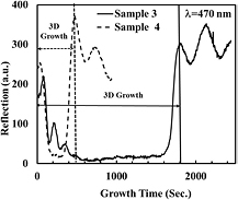
Figure 3. Reflectivity recorded during the growth of sample 3 and sample 4.
Download figure:
Standard image High-resolution image
Figure 4. Improvement in surface morphology through a 3D growth process: (a) sample 4, with a shorter 3D growth process; (b) sample 3, with an intensive 3D growth process. The random defect shown in figure 3(b) is used as a reference for taking the SEM image.
Download figure:
Standard image High-resolution imageThe elimination of hillocks by growing a thick 3D GaN layer bears a marked similarity to the dislocation annihilation and bending process observed in GaN layers grown on PD substrates by epitaxial lateral overgrowth (ELOG) [14]. Specifically, a high density of extended defects in the nucleation layer will penetrate a growing GaN layer and lead to the formation of grains with significant tilts and/or twists, which result in the occurrence of facets, such as GaN(1 0 –1h) (h = 0, 1, 2, 3.....). These facets grow at different rates and consequently the surface becomes rough, as seen in figure 4(a). A prolonged 3D growth process will eliminate many of these facets caused the expansion of the slow growing crystallographic facets, at which point the strain can be released locally. The resulting strain gradient can then cause dislocations to bend, interacting to annihilate each other, to result in a more ordered epitaxial film.
This can be seen in figure 5 which compares the x-ray rocking curves of samples 3 and 4 for (a) GaN(10  3) and (b) GaN(0 0 0 2) diffraction. The twist in sample 3 is smaller than that in sample 4 (figure 5(a)) as a result of its thicker 3D GaN layer. Similarly the tilt in sample 3 is smaller than in sample 4, reduced to 0.35°compared with 0.71° tilt in sample 4 (figure 5(b)).

Figure 5. Rocking curves of sample 3 and sample 4: (a) GaN(1 0 − 1 3), twist and (b) GaN(0 0 0 2), tilt.
Download figure:
Standard image High-resolution image3.3. Tensile stress control
As a result of the high CTE of GaN compared to that of diamond, a mismatch of ~27% [18], a high tensile stress in the GaN layer will develop on cooling from the growth temperature to room temperature. Stress control techniques, such as inserting an AlGaN multilayer stack between an AlN nucleation layer and a GaN layer, or using an intermediate AlN layer between two neighbouring GaN layers, are useful for the growth of crack-free, light–emitting diodes on a Si(1 1 1) substrate, because the much-reduced stiffness of Si [19] at temperatures above 1000 °C allows the Si substrate to bow, according to the Stoney equation [20, 21]. Such an approach may not be appropriate for the growth of GaN layers on PD since the stiffness of the PD barely changes with temperature [22], while the effect that pseudomorphic compressive strain deliberately introduced during epitaxial growth will not cause the substrate to bow in a way that compensates for the tensile stress induced by the CTE mismatch during cool-down. Instead, strain relief by forming misfit dislocations, or worse, cracking, is more likely. Further, as the thermal conductivity of AlGaN is small, about 1% of that of diamond [23], any AlGaN layer introduced into the buffer layer of a device will degrade the thermal resistance between it and the substrate [24].
Dadgar et al have reported that a 3D growth process can also be used to generate a compressive stress by increasing the GaN grain size through growing it on a SixN-mask formed in situ on a low-temperature AlN nucleation layer [25]. The procedures used in growing samples 3 and 4, with their initial 3D growth step at ∼800 °C, were, in effect, a modified version of the approach of Dadgar et al, but without the SixN layer, which was omitted in order to eliminate its contribution to thermal resistance between the 2D GaN layer and the PD substrate. Further, it has been shown that the wavenumber of the E2H mode of the Raman scattering spectrum of GaN provides a sensitive measure of strain in the layer structure [26]. This technique has been used to assess in samples 3 and 4 the impact of their different duration 3D growth steps, hence GaN grain size, on reducing CTE mismatch strain in GaN epitaxial layers grown in PD substrates.
Figure 6 shows the Raman scattering spectra in the region of the E2H phonon mode of the two samples. The GaN layer of both samples is under tensile stress, but the greater thickness (∼900 nm) of the 3D GaN layer in sample 3 has caused a shift of ~1.5 cm−1 of the E2H phonon peak towards the zero strain position of 568 cm−1, compared with its position for sample 4. The rate of shift of the E2H peak with biaxial strain in GaN epitaxial films has been reported to lie between a theoretical value of 2.4 cm−1 GPa−1 and measured values in the range 2.7–6.2 cm−1 GPa−1 (for a review, see 26). Tripathy et al reported a coefficient of 4.3 cm−1 GPa−1 for the strain-induced shift of the E2H phonon peak in GaN and AlxGa1−xN/GaN heterostructures grown on Si(1 1 1) [27]. Using the latter value on the basis that it was obtained from hetero-epitaxial structures under tensile stress as our data were, the reduction in tensile stress resulting from the more extensive 3D growth is estimated to be ∼350 MPa.

Figure 6. Raman spectra of samples 3 and 4 in the vicinity of the E2H phonon mode.
Download figure:
Standard image High-resolution imageThe tensile stress in an as-grown GaN layer can also be reduced by utilising the inherent bow of PD substrates. The origin of this curvature of the PD is residual stress developed in the PD during its growth on the silicon substrate [28]. Because of the high thermal conductivity of diamond, the curvature is not expected to lead to a significant temperature variation across a PD substrate during GaN epitaxial growth, particularly when an appropriately curved substrate holder is used. The convex bow of PDA type substrates is preferred because this will tend to compensate the higher CTE of GaN on cool-down from its growth temperature. Figure 7 compares the Raman scattering spectra near the E2H peak of samples 5 and 6 which were on PDB and PDA, i.e. substrates of opposite curvature, respectively. Apart from the different sign of the substrate bow, the growth parameters of these samples were the same as those of sample 3, except that the thickness of the AlN nucleation layer grown at ~800 °C was increased to 40 nm.

Figure 7. Raman spectra in the vicinity of the E2H phonon mode for (a) sample 5 grown on a concave PDB substrate and (b) sample 6 grown on a convex PDA substrate.
Download figure:
Standard image High-resolution image
Despite samples 5 and 6 both having concave curvatures after growing the III-nitride heteroepitaxy, the E2H peak in the Raman scattering spectrum of samples 6 is ~1.8 cm−1 closer to its unstrained wavenumber, a shift (based on the data in [27]) that corresponds to a tensile stress ~420 MPa lower than that in sample 5. Further, no cracks were observed in sample 6, whilst some scattered cracks appeared in sample 5. The reduced tensile stress in sample 6 is related to its curvature change from convex to concave during cooling down. The curvature flip, from convex to concave before and after growing the III-nitride heteroepitaxy, occurs because the PDA substrates are only 50–60 µm thick (as were the PDB substrates) and therefore less rigid than thick diamond substrates (>0.2 mm). As such, they were thin enough to be deformed on cool-down from the GaN growth temperature. This use of flipping the pre-existing wafer bow provides a promising method for mitigating CTE induced tensile stress in GaN epitaxy grown of PD substrates, but needs detailed characterisation and modelling.
4. Conclusions
A method for growing epitaxial GaN/AlGaN heteroepitaxial layers on low-cost PD substrates of high thermal conductivity has been demonstrated. The method exploits the presence of a thin SixC layer formed during the deposition of PD on Si(1 1 1) for providing sufficient crystallographic information for the epitaxial growth process to occur. A 3D growth process has shown to be effective in removing the surface defects that are induced by the non-single crystalline nature of the SixC layer and to reduce the tensile stress induced by a thermal expansion mismatch. A novel approach that utilises the residual convex curvature found in some PD substrates has been demonstrated to further reduce the tensile stress, to result in crack-free GaN epitaxial layers up to 1.1 µm thick. The twist and tilt can be as low as 0.65° and 0.39°, values broadly comparable with GaN grown on Si substrates at an equivalent stage in technology development [29]. Neither the 3D GaN growth process nor the convex pre-bow of the PD substrate have been optimised, and therefore there is the prospect of further reductions in the tensile strain inherent in GaN epitaxial layers grown on PD. Any increase in GaN epitaxial layer thickness is usually accompanied by reductions in the density of threading defects, which in turn will improve device performance. As such, this work demonstrates the prospect of growing epitaxial GaN layers with low defect density directly on high thermal conductivity and low-cost PD substrates to extract heat from devices in which electrical power dissipation can be high.
Acknowledgment
This work was supported by the Engineering and Physics Sciences Research Council of the United Kingdom under grant number EP/K024337/1.
All data created during this research are openly available from the University of Bath data archive at https://doi.org/10.15125/BATH-00328