

Abstract
Science and technologies based on terahertz frequency electromagnetic radiation (100 GHz–30 THz) have developed rapidly over the last 30 years. For most of the 20th Century, terahertz radiation, then referred to as sub-millimeter wave or far-infrared radiation, was mainly utilized by astronomers and some spectroscopists. Following the development of laser based terahertz time-domain spectroscopy in the 1980s and 1990s the field of THz science and technology expanded rapidly, to the extent that it now touches many areas from fundamental science to 'real world' applications. For example THz radiation is being used to optimize materials for new solar cells, and may also be a key technology for the next generation of airport security scanners. While the field was emerging it was possible to keep track of all new developments, however now the field has grown so much that it is increasingly difficult to follow the diverse range of new discoveries and applications that are appearing. At this point in time, when the field of THz science and technology is moving from an emerging to a more established and interdisciplinary field, it is apt to present a roadmap to help identify the breadth and future directions of the field. The aim of this roadmap is to present a snapshot of the present state of THz science and technology in 2017, and provide an opinion on the challenges and opportunities that the future holds. To be able to achieve this aim, we have invited a group of international experts to write 18 sections that cover most of the key areas of THz science and technology. We hope that The 2017 Roadmap on THz science and technology will prove to be a useful resource by providing a wide ranging introduction to the capabilities of THz radiation for those outside or just entering the field as well as providing perspective and breadth for those who are well established. We also feel that this review should serve as a useful guide for government and funding agencies.
Export citation and abstract BibTeX RIS

Original content from this work may be used under the terms of the Creative Commons Attribution 3.0 licence. Any further distribution of this work must maintain attribution to the author(s) and the title of the work, journal citation and DOI.
Corrections were made to this article on 05 01 2017. The author affiliations were updated in the main author list and chapter headings.
1. Terahertz quantum cascade lasers
S S Dhillon1, M S Vitiello2, E H Linfield3 and A G Davies3
1 Laboratoire Pierre Aigrain, Ecole Normale Supérieure-PSL Research University, CNRS, Université Pierre et Marie Curie-Sorbonne Universités, Université Paris Diderot-Sorbonne Paris Cité, 75231 Paris, France.
2 NEST, CNR—Istituto Nanoscienze and Scuola Normale Superiore, Piazza San Silvestro 12, 56127 Pisa, Italy
3 School of Electronic and Electrical Engineering, University of Leeds, Leeds, LS2 9JT, UK
Status.
Quantum cascade lasers (QCLs) are compact semiconductor sources exploiting III–V superlattice materials that were first demonstrated in the mid-infrared (mid-IR) and, since 2002, in the THz frequency range [1]. Laser action arises from transitions between electronic subbands formed in a series of quantum wells and, by 'cascading' a number of such active regions together, the injected electrons undergo multiple lasing transitions as they pass through the device (see figure 1a). The entire characteristics of the laser can therefore be controlled through bandstructure engineering and by the design of the semiconductor superlattice. The QCL concept has enabled powerful and compact sources to be realized in previously inaccessible regions of the electromagnetic spectrum. In the mid-IR, QCLs have achieved impressive performance levels with multi-Watt output power, room temperature (RT) and continuous wave (CW) operation with wall-plug efficiencies of up to 21% at RT, and can cover a wide spectral range of 2.7–25 µm. Beyond the Restrahlen band (>50 µm), QCLs have also shown remarkable performances over the range 1–5 THz range, with demonstration of high powers (>1 W), photonic and far-field engineering, a quantum limited linewidth, frequency combs and pulse generation [2]. These advances have permitted THz QCLs to be made commercially available and, although cryogenic cooling is still required, this can be achieved conveniently and inexpensively with Stirling coolers. A wide range of applications are now being targeted from local oscillators for astronomy, to use in metrology and non-destructive imaging [2]. Although there remain challenges, the further development and exploitation of THz QCLs is crucial owing to the unparalleled success of these devices in terms of their output power and wavelength agility in a compact, potentially inexpensive and user-friendly geometry.
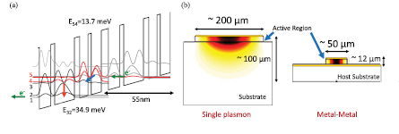
Figure 1. (a) Bandstructure of two periods of an LO phonon depopulation-based QCL active region for emission at 3.3 THz (13.7 meV, electronic states 5 and 4). (b) Modal profile of the two waveguides used for THz QCLs: single plasmon, where the THz mode is weakly confined and has a large overlap with the substrate; and, metal–metal, where the mode is strongly confined between two metal layers.
Download figure:
Standard image High-resolution imageCurrent and future challenges.
After a decade of research, the operation temperature of THz QCLs has progressively risen to 199.5 K in pulsed mode [3] (and in the absence of an applied magnetic field), although this maximum temperature has stayed static now for a number of years. The GaAs/AlGaAs material system and active region designs are likely to be the limiting factors. Although commercial systems exploiting such QCLs can be based around Stirling coolers, for more mainstream applications and lower cost, Peltier cooling would be beneficial. However, this will require an increase in the current maximum operating temperature to around 240 K.
An alternative methodology is to leverage advances in high-power two-colour mid-IR QCLs for room temperature, intra-cavity THz difference frequency generation [4]. Although the emission is not as powerful as from THz QCLs, this route has shown intriguing breakthroughs in temperature operation and tunability. A challenge here is to overcome the wall-plug efficiency limit, which is at best just ~10−6.
Two types of THz QCL waveguides are implemented: the surface plasmon (single metal) waveguide, and the metal–metal (MM) waveguide (Figure 1b). The latter is beneficial for higher temperature operation, and for lower QCL frequency operation, although at the cost of a poorer output beam profile and lower output power. Initial efforts to address this employed facet-mounted lenses, horn-antennas and photonic crystals. Nonetheless, these do not simultaneously satisfy the requirements of monolithic geometry, high power and a controlled far-field radiation profile. Photonic heterostructured and 3rd order DFB geometries currently provide potentially valuable solutions to address this challenge [5]. These approaches, however, are all frequency-selective in nature, and are therefore not appropriate for broadband coupling that would be required for future challenges such as broadband amplifiers, pulse generation and frequency combs (see below). Broadband, efficient integrated couplers for THz QCLs therefore represent an important future goal, particularly operating at very high powers.
Tuning of the QCL frequency emission is also an important challenge. Although the spectral linewidth of the QCL [6] is ideal for gas spectroscopy, tuning remains non-ideal. Although a range of solutions have been realized including through temperature control, multi-section DFB structures [7], and Vernier tuning [8], the tuning range is proving to be limited. An important step would be the realization of an external cavity with a THz QCL gain medium. For this, efficient anti-reflection coatings that can cover a large spectral range need to be developed.
The investigation of schemes for developing broadband THz QCL frequency combs (FCs), is a topic of considerable current interest [9, 10] where the compensation of the index dispersion over a large frequency range is vital. Complementary to this is short pulse generation from QCLs, where currently 10 ps pulses can be generated at best, with relatively low output powers [11, 12]. This is a direct consequence of the ultrafast QCL dynamics. Future development will be needed to meet the challenge of simultaneous generation of much shorter pulses with high powers through new modelocking geometries.
An important challenge will be to bring these developments in source technology towards systems, requiring new approaches to THz detection in terms of rapidity and sensitivity at high temperatures. Promising directions include self-mixing, down- and up-conversion, and nano-detection technologies (QWIPs, nanowires or quantum-dot approaches). This will work towards complete THz systems, promising breakthroughs in optical communication, quantum computing, dual-comb spectroscopy and time-of-flight tomography.
Advances in science and technology to meet challenges. Given the temperature performance ceiling of current THz frequency QCLs based on the GaAs/AlGaAs materials system, other semiconductor materials such as InGaAs and InAs have gained attention, not least owing to their lower effective masses and therefore higher gain. High quality growth with control of the optical losses is vital here, however. More exotic systems currently being explored include SiGe heterostructures, III-nitride quantum wells and even II–VI systems. The latter two materials have large LO phonon energies (>70 meV) and so the major bottleneck for high-temperature operation (thermally activated LO-phonon scattering) should be dramatically suppressed. An even more radical approach to suppress non-radiative scattering is to implement a cascade laser within a series of quantum-dots, rather than through quantum-wells. This would potentially result in zero energy dispersion in momentum space, thus reducing non-radiative scattering [13]. Both top-down and bottom-up investigations of quantum-dot patterning are being made or have been proposed, with the former dependent on improvements in advanced processing techniques and surface passivation, and the latter requiring new growth techniques such as in situ site-controlled dots.
In the context of room temperature intracavity THz difference frequency generation, this would benefit from advances in mid-IR QCLs with a shift towards shorter mid-IR wavelengths (~5 µm) that show better wall-plug efficiency that will directly improve the THz output power. Although the current geometry relies on the Cherenkov coupling scheme, and is efficient in extracting the THz radiation, the use of both passive waveguides and more traditional phase matching schemes may allow the realization of an electrically pumped chip-based THz optical parametric oscillator.
To address the ambition for integrated spectrometers and broadly tunable sensing systems, different technological solutions can be envisioned: arrays of vertical-emitting ring-cavities or distributed feedback lasers in master-oscillator power amplifier configurations [14], and heterogeneous QCLs in external cavity systems, represent, respectively, very promising solutions. A possible option for broadband, efficient integrated THz out-couplers could be the exploitation of quasi-periodic structures (1D gratings, 2D quasi-crystals) or even random resonators to break the symmetry of the radiating modes [15]. In terms of THz QCL tunability, extremely narrow double-metal cavities combined with refined MEMS systems [16] or surface-emitting resonators in coupled microcavity architectures, exploiting metallic mirrors, graphene or metamaterials have potential. Finally, to address the development of a broadband QCL FC, group velocity dispersion can be significantly reduced through new active regions, waveguide designs, and integrated chirped mirrors. Short pulse generation via mode-locking [17] can also take advantage of these advances and by implementing hybrid active-passive approaches or by devising suitable saturable absorber components with novel architectures, or by exploiting novel, still unexplored materials, with appropriate THz absorption features.
Concluding remarks.
Although there remain considerable challenges ahead, THz frequency QCLs are currently the only compact source operating with high output powers above 1 THz. Through the potential advances highlighted above, further applications and functionalities of these devices will be found ranging from fundamental science to applied research, including their use as new sources for nonlinear optics, imaging, spectroscopy and trace gas analysis, inter alia. There remain open questions on the operation of these devices, including their high temperature performance, their dynamics related to pulse generation, and the possibility to realize extremely broadband frequency combs. Further, QCLs will accompany new advances in detector technology, such as coherent detection and nano-detection techniques, to provide powerful, inexpensive and compact THz systems.
2. Intense laser-based THz sources
Matthias C Hoffmann
Linac Coherent Light Source, SLAC National Accelerator Laboratory, Menlo Park, CA 94025, USA
Status.
The spectral range between 0.3 and 30 THz has long been described as the 'THz gap' because of the lack of strong and compact sources. This has changed drastically in the last two decades. CW-sources based on microwave technology (see summary in section 6) and solid state sources based on quantum cascade laser technology (see section 1) are now available and offer average power in the mW range. Dramatic improvements have also been made in the generation of intense picosecond THz pulses via nonlinear optical methods such as optical rectification [25]. It is now possible to routinely generate pulse energies of tens of micro-joules and field strengths exceeding 1 MV cm−1 with a compact and reliable femtosecond laser source in a small university laboratory without issues of restricted access, low repetition rate, timing stability and beam transport issues in accelerator-based THz facilities.
The most promising applications of these strong-field THz sources are in basic science. Here, researchers take advantage of the fact that resonant excitation in the THz and far-infrared range can be used to selectively deposit energy into specific low frequency modes of the material. This is of great importance to study non-equilibrium dynamics of complex matter such as unconventional superconductors, multiferroics and magnetic materials [18] and semiconductors (see section 9). Femtosecond laser pulses typically have wavelengths in the visible or near-infrared range, and have photon energies in the range of 1–2 eV, well above the band gap energy of many complex materials. Pumping materials directly at these photon energies result in a cascade of photo-induced processes that can obscure the more subtle low energy phenomena. Various optical, THz or ultrafast x-ray probe techniques can then be used to study the response of the system. New ways of understanding collective phenomena are possible when the coupling between electronic, spin and vibrational degrees of freedom is untangled. This has been demonstrated successfully in several mid-infrared pump experiments, where direct control over a structural phonon is exerted by the laser [19].
A further avenue to control complex materials is to take advantage of the high peak magnetic fields present in a THz pulse which can approach 1 T, enabling ultrafast control of magnetism.
Current and future challenges.
A schematic overview of currently available THz sources is shown in figure 2. Present laser-based sources are able to produce single-cycle pulses centred at 1 THz or quasi-single cycle centred at 2 THz with peak fields on the order of 1 or 2 MV cm−1. The two main techniques are optical rectification in LiNbO3 with tilted pulse front (TPF) pumping [21] or optical rectification in organic crystals with an extremely high nonlinear constant χ(2). The TPF technique can be deployed with various pump wavelengths and powerful Ti:Sapphire or Yb:YAG lasers can be used at their fundamental wavelengths to drive the rectification process. Scaling to high average power/high repetition rate is also possible. The spectral content of the resulting THz pulses is limited to <3 THz by material absorption. Organic nonlinear crystals like DAST, DSTMS, OH-1 etc can be used for optical rectification in a collinear geometry [22]. These materials have extremely high nonlinear coefficients and thus lead to very good conversion efficiency. Phase matching and material absorption however requires pumping at near-infrared wavelengths of 1200–1500 nm which are nonstandard for commercial femtosecond laser systems without additional wavelength conversion. The spectral content is typically higher and again determined by the location of phonon modes in the conversion crystals. A drawback is the low damage threshold (~1 mJ cm−2) at high laser repetition rates due to thermal effects and the limited availability of large area crystals. For both optical rectification techniques the photon conversion efficiency can exceed 100% due to the cascaded nature of the process. This can lead to problems with spectral depletion, affecting the pump laser intensity front [26].
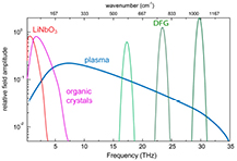
Figure 2. Overview of intense laser-based THz sources: optical rectification in LiNbO3 or nonlinear organic crystals results in broadband, single-cycle pulses. Ionization of plasmas produce ultra-broadband pulses with a wide frequency spectrum. Difference frequency mixing (DFG) of optical parametric amplifiers delivers narrowband tunable mid-infrared pulses.
Download figure:
Standard image High-resolution imageTunable, phase stable multicycle pulses in the mid-infrared (15–30 THz) region can be efficiently obtained via difference frequency generation processes in materials such as GaSe [23]. Since the wavelengths are inherently shorter, much higher peak field strengths (>100 MV cm−1) can be achieved due to tighter focusing. Finally, asymmetric ionization processes in plasmas can be used to produce short ultra-broadband pulses covering a wide frequency spectrum reaching well into the infrared [20], but with relatively low field amplitude per frequency unit.
To study effects far from equilibrium with low THz frequencies single-cycle pulses at will require roughly a tenfold increase in field strength at the sample.
Currently, no intense laser-based sources currently exist which provide tuneable multicycle THz radiation in the range of 5–15 THz. The existence of such sources is crucial to resonantly excite optical phonons or other collective modes in this important frequency range. This new 'THz gap' will be a major challenge for source development in the coming years.
Advances in science and technology to meet challenges.
A major research direction in the coming years will be scaling up the energy of single-cycle THz pulses to reach 100 µJ–1 mJ pulse energies at ~1 THz, and associated peak field levels that approach 10 MV cm−1. Such a source will have a direct scientific impact by overcoming the peak field strength limit and compete directly with electron-beam based single- cycle methods. Development will be relatively straightforward and use scaling of existing techniques by using larger area size crystals, stronger laser sources and improved cooling. For rectification in organic crystals this will likely entail the use of new femtosecond laser technologies in the 1200–1500 nm wavelength range such as Cr:Forsterite lasers, and large area mosaics of nonlinear crystals to avoid damage [24].
Generation of intense, narrowband and tuneable pulses in the region of 5–15 THz will present a formidable future challenge. Such a source addresses a current unmet need in materials science applications where resonant excitation with moderate to high field strength is needed. One possible option will be using a difference frequency generation scheme with picosecond laser pulses. This will require tailored laser sources as well as novel nonlinear materials with high χ(2) and transparency window for phonon absorption. Alternative solutions might entail quasi-phase matched optical rectification, again requiring research and development of suitable nonlinear materials providing adequate phase matching, low THz absorption, high damage threshold and high nonlinear constants.
Concluding remarks.
Laser based intense THz sources have progressed tremendously in the last decade. They are now being used to study materials in THz pump experiments that have been previously impossible. Scaling up of current single sources will enhance our understanding of material behavior in the limit of extremely strong THz pulses, where the instantaneous electromagnetic fields exceed the DC breakdown values by a significant amount. Developing tailored pump solutions in the 5–15 THz range will enable novel avenues of control in complex material systems by targeting low energy collective phenomena directly. The future of THz science looks bright indeed.
3. THz vacuum electronics
John Booske1, Claudio Paoloni2,
1 Electrical and Computer Engineering Department, University of Wisconsin - Madison, 1415 Engineering Drive, Madison, WI 53706, USA
2 Engineering Department, Lancaster University, Lancaster, LA1 4YR UK
Status.
After 110 years, the oldest electron device, the vacuum tube, has evolved from kHz to THz and mW to MW, as the only practical device for many important applications requiring efficient, compact, medium-to-high power, long-operating-life electromagnetic radiation sources [27]. Vacuum electronic devices (VEDs) convert electrical stored energy into kinetic energy of an accelerated electron beam, which is then converted into electromagnetic field energy with the aid of electromagnetic waveguides or cavities, defined as an interaction zone or circuit (figure 3) [28]. Presently, numerous types of VEDs are available, including traveling wave tubes (TWTs), klystrons, magnetrons, gyrotrons and backwards wave oscillators (BWOs), for applications in satellite communications, radar, remote sensing and threat detection, electronic warfare, domestic cooking, industrial heating, space exploration, and scientific research [29, 30]. Generally, the highest attainable frequency is determined by fabrication technologies and the theoretical scaling relation  [27, 28]. Due to physical limits on power density management, VEDs present the only practical solution for high power, compact, efficient sources (oscillators, amplifiers) of 0.1–1.0 THz radiation [27–31]. VED oscillators and amplifiers (figure 4) have been designed and operated at 0.220–1.0 THz and 10 mW–1 MW with high efficiencies (0.5–20% and above) [29–34]. Such performance is unachievable by any other technology [27]. The ability to achieve exceptionally high overall efficiency by spent beam energy recovery is uniquely available to VEDs and not possible with any other compact THz radiation source [28]. Further advances in 0.1–1.5 THz wideband amplifiers and oscillators with watt-level power sufficient to overcome atmospheric attenuation, and dimensions in the range of a few dm3, will enable new generations of multigigabit mobile communications networks (see section 17) and high resolution radar or remote sensing systems that are able to penetrate fog, dust, or other aerosols that obscure shorter-wavelength technologies. Other applications of future high power THz-regime VEDs will include stable frequency sources for imaging (see section 15), deep space communications, non-invasive healthcare diagnosis (see section 12), materials characterization (see section 13), radio astronomy (see section 14), and other scientific research technologies [27–31].
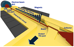
Figure 3. Conceptual illustration of a THz vacuum electron amplifier, including the gun (electron beam source), interaction circuit, beam confinement magnets t, beam collector and radiation ports. Oscillators would not need the input port.
Download figure:
Standard image High-resolution image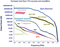
Figure 4. State of the art of compact and gyro THz vacuum electron devices. Data for compact sources (TWT, BWO, EIK, magnetron) from [29–31]. Data for gyro devices from [32]. The two thick, double-banded, continuous lines represent the upper performance limit bounds (to date) of the compact sources and gyro devices, respectively.
Download figure:
Standard image High-resolution imageCurrent and future challenges.
In compact VEDs based on classical physics mechanisms, the cross-sectional size of the circuit must scale with the free space wavelength. Therefore, to populate the THz gap, the transverse circuit dimensions of VED sources will typically need to be less than the free space wavelength, i.e. sub-mm [27–31]. Consequently, current and future challenges for compact THz VED sources involve reliably manufacturing miniature VED circuits that generate and tolerate high internal densities of beam and radiation power. Moreover, to minimize power dissipation, conducting surfaces will need excellent surface quality, including low impurity concentrations, low surface roughness (<20 nm) and moderate grain size (>100 nm) [33]. This means that innovations and advances are needed in the following areas:
- Reliable manufacturing of miniature electromagnetic structures (cavities, slow-phase-velocity waveguides) having high quality surfaces and compatible with hard vacuum, high temperature thermal processing during manufacture, and highly precise alignment accuracy (micron-level or <0.1 degree) between components (cathode, beam optics, electromagnetic circuit, and beam collector)
- Designs for high current electron beams with sub-mm cross-sections, at least in one transverse dimension
- New cathodes that enable high current density, small cross-section electron beams with long lifetimes and lower cathode temperatures [28–30, 35]
- Novel circuit designs having strong beam-wave interaction at THz frequencies with low voltage electron beams
- Compact, low-power, beam optics and confinement, keeping the beam away from impact on structure walls
- Efficient, broadband coupling of radiation out of the circuit (oscillators and amplifiers) and into the circuit (amplifiers)
- Innovative electromagnetic circuit designs with larger cross-sections that still provide stable, high power, efficient generation or amplification of THz-regime radiation.
Advances in science and technology to meet challenges.
A new age of opportunity for THz-regime VEDs has emerged with the maturation of highly precise, highly accurate microfabrication techniques. These include extensions of conventional machining, such as nano-CNC milling, laser-machining, and micro-electro-discharge machining (micro-EDM), as well as the suite of lithographically-controlled etching, deposition and assembly techniques derived from micro-electro-mechanical systems (MEMS) research [29, 34]. Examples of the latter include deep reactive ion etching (DRIE), x-ray or ultraviolet LIGA (LIGA is a German acronym for lithography and molding), metallic and dielectric film deposition and diffusion bonding with substrate backside alignment [28]. The other recently emergent enablers are the numerous, exceptional advances in computational hardware, algorithms, and software. High performance, high throughput terascale computing is a stable, established technology. Highly sophisticated, 1-, 2-, and 3D, time-dependent, multiphysics models of electromagnetic fields, charged particle transport, thermal physics and engineering mechanics have been developed and validated, resulting, in many cases in 'first-pass' design success [28, 31]. These simulation codes now permit quick and accurate predictive evaluation of innovative ideas prior to expensive experimental prototyping and validation.
To realize more powerful, compact, VED sources of THz radiation, scientists and engineers will need to leverage these new fabrication and simulation capabilities and also achieve innovations in electromagnetic THz circuits, beam optics, cathodes, materials and metrology. New circuits exploiting metamaterial or photonic crystal architectures might loosen the requirement for close beam-circuit proximity and still achieve strong beam-wave interaction [31]. Higher current density cathodes or advanced beam diode focusing optics would enable transporting higher beam power into the very small THz electromagnetic circuit cross-sections [27, 29, 31, 36]. An alternative solution for high power beams in small THz circuits is to generate and focus innovative distributed beams, either laminar sheets or multiple beamlets, that are small in one cross-sectional dimension but spread the current out in the other cross-sectional dimension [27, 31]. This requires new electromagnetic circuit ideas as well as well-designed magnetic focusing fields to avoid beam instability or to stably guide the many beamlets, respectively. Advances in permanent magnet materials or high temperature super-conductors would enable better magnetic focusing optics with less weight and size. The availability of high-current-density, long-lifetime cold cathodes would enable low-cost, self-aligned integration of the cathode, circuit, and collector during mass production manufacturing of micro-VEDs [28, 30]. Advances in metallic 3D printing or new alloys for electroplating would provide more options for miniature circuit fabrication. However, the materials and processes would need to yield a circuit with dimensional features <100 µm, tolerance precision ~1 µm, high THz conductivity >  S m−1, surface finish <20 nm [33], and stability against grain growth or stress-induced deformation during high-temperature thermal processing at hundreds of °C. Finally, advances are needed in metrology to characterize and verify the electromagnetic resonances or dispersion of THz circuits, precision alignment of components, magnetic field profiles inside the circuits, input and output radiation coupling efficiencies, and the structural, microstructural and electromagnetic properties of the circuit materials before and after manufacturing processes.
Concluding remarks.
The progress toward compact, low weight, reliable, affordable, medium-to-high power THz vacuum electron devices (VEDs) is a fascinating adventure in a state-of-the-art, multidisciplinary field. The combined effort of a growing number of research groups active worldwide is yielding new designs, materials and fabrication methods to overcome the formidable obstacle posed by high-power-density VEDs with submillimetre dimensions. The future availability of low cost, high-power-density, THz VED sources will enable transformative advances in the world of THz applications, where the power, size, weight, availability and/or cost of present device options limit the outstanding and unique potential of THz radiation.
4. Accelerator-based sources of terahertz radiation
M Gensch1, P Weightman2 and G P Williams3
1 Helmholtz-Zentrum Dresden-Rossendorf, Institute of Radiation Physics, Bautzner Landstr. 400, 01328 Dresden, Germany
2 Physics Department, University of Liverpool, Liverpool, L69 7ZE, UK
3 Jefferson Laboratory, 12000 Jefferson Avenue—Suite 21 Newport News, VA 23606, USA
Status.
The potential of accelerator driven sources of electromagnetic radiation for scientific research across a wide variety of fields has long been recognized, and exploited internationally, most notably through the development of synchrotron storage rings into unique, broad band multi-user facilities for spectroscopy in the VUV to x-ray regime. The last three decades have seen increasing user interest in utilizing accelerator driven sources for research in the infrared and THz regime. The primary advantages of these sources over table-top sources, such as those described in sections 1 and 2 derive from their unique spectral brightness or power and their extreme fields and pulse energies. Historically the first applications of accelerator driven sources exploited the high spectral brightness and power available from infrared beamlines at storage rings [37], followed quickly by the use of dedicated user facilities such as IR/THz free electron lasers [38] and finally superradiant radiation [39], where the bunch length of the electrons is less than the wavelength of the emitted radiation, from energy recovery linacs (ERLs) [40]. The primary applications of this first generation of sources are brightness-limited spectroscopic techniques such as far-field microscopy or investigations of processes that require high average power such as action spectroscopy [41] or power-limited spectroscopic studies of e.g. biological systems in water [42]. In the past decade there has been increasing interest in utilizing the extreme scalability of the energy per THz pulse in compact linear accelerator (linac) driven sources. The scientific driver here is research aimed at understanding ultrafast THz driven nonequilibrium dynamics in matter [43] (figure 5). The vision to provide electric fields in the V/Å regime, comparable to the dipole field of an ionic bond, or magnetic fields in the few T regime, commensurate with fields required for alignment of magnetic domains, has led in recent years to considerable technological efforts worldwide [44].
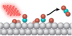
Figure 5. THz-driven chemistry—a quasi-half-cycle, broadband superradiant THz pulse with peak fields of ~1 V nm−1 (10 MV = cm) and a peak frequency of 10 THz induces CO oxidation on the coadsorbed phase of CO and O on Ru(0 0 0 1) in ultrahigh vacuum (UHV) at a temperature of 300 K [50] (reused by permission of H Ogasawara/SLAC and APS/Joan Tycko)).
Download figure:
Standard image High-resolution imageNumerous accelerator-based THz sources are operational worldwide as user facilities. The most common sources are synchrotron infrared beamlines [37] that are available on many synchrotron storage rings. Although the performance of laser-based sources and sources based on thermal emitters in their typical frequency range, 1–30 THz, has improved tremendously in the past 10 years, infrared synchrotron beamlines are still very competitive for brilliance limited spectroscopic techniques such as infrared microscopy and ultra-broadband infrared near-field microscopy. Some storage rings can be operated in a special operational mode, called low alpha mode, which via shortening the electron bunches to the few picosecond regime employ superradiant emission to achieve substantial increases in spectral power below 1 THz [39]. In this mode of operation average powers in the few 10 mW regime have been demonstrated and several breakthrough experiments on spectroscopy in correlated materials have been performed (see e.g. [45]). Other projects have used external lasers to slice or to modulate the electron bunch structure to induce superradiant THz emission [46]. The first ERL source became operational in 2001 [40], and these sources provide radiation in a similar frequency range and with significantly more power than can be obtained on a synchrotron. Average powers of the order of 10 W and peak powers in the kW regime have been obtained. This is possible because they are based on the new superconducting radio frequency (SRF) technology that enables the operation of linear accelerators at previously unprecedented duty cycles. There are few operational facilities but the potential of these sources has been demonstrated in a number of experiments [42, 47]. There is a much wider use of low-gain free electron lasers. Their pulsed, narrow-band tunable radiation is used in the chemical and life sciences to study the infrared spectrum of dilute systems such as clusters or individual molecules by means of the so called action spectroscopy [41]. Some facilities use SRF technology and hence provide average powers in the few 10 W to even kW regime. Those focus on specific spectroscopy applications in solid state physics that benefit from high flux such as nearfield microscopy [48] or studies of samples under extreme conditions e.g. high pressure or high magnetic fields [49]. The combination of an ERL and a THz FEL provides a particular high power source tunable over a narrow frequency range.
Current and future challenges.
The operation of synchrotrons in the low alpha mode degrades the output of the accelerator in the shorter wavelength regions that are required for experiments by a large user community and as a result the allocation of time to this mode of operation is limited. It is possible to make further improvements to the performance of synchrotrons in this spectral region but given the recent advances in the performance of laser based THz spectroscopy sources it is not clear that synchrotron THz sources will remain competitive in the future. A class of linac driven superradiant high-field THz sources is emerging [44] that, unlike low-alpha synchrotron storage rings and ERLs, aims at generating high THz fields from highly charged electron bunches and these are finding applications in investigations of ultra-fast THz-field driven non-equilibrium dynamics. The emitted pulses are carrier-envelope phase stable and, in principle, the design allows the operation of many different types of radiators in parallel from one electron beam. This has the potential to provide a multitude of THz pulse parameters ranging from single-cycle (transition and diffraction radiators) to multi-cycle (undulators) to extreme narrow bandwidth (corrugated waveguides) [44]. The obvious advantage of this design over laser-based sources is its inherent scalability with respect to the achievable field and/or repetition rate. Although no operational user facility yet exists, several successful pilot experiments have been performed on test facilities and have established the potential of this type of source for investigating THz driven non-equilibrium dynamics in matter in a completely new field regime, one recent example being THz selective control of surface chemistry [50]. The record THz fields have so far have been obtained at large linear accelerators and at relatively low repetition rates [51] limiting the application to a few demonstration experiments [50]. A general challenge for time-resolved experiments at accelerator-based THz sources like FELs or superradiant linac-based sources, remains the synchronization to external laser systems which is currently limited to the few picosecond regime.
Advances in science and technology to meet challenges.
There has recently been a proposal for a novel variable pulse length storage ring concept [52] which if successful would make it possible to generate THz pulses using the low alpha mode on a synchrotron while preserving the beam properties for the typical XUV and x-ray applications. This would result in a significant increase in the available beamtime on synchrotrons for applications in the low THz frequency range. In the field of linac-based superradiant high-field THz sources there are more than ten projects that are currently proposed or are being developed worldwide based on the development of compact sources of high-field THz radiation. Sources with linacs of only a few meters in length are proposed or are already being commissioned [44]. Some projects aim to combine high fields of the order of MV cm−1 with high repetition rates up to the MHz regime. These sources are based on compact quasi-continuous wave SRF linac technology and have demonstrated impressive progress. Since SRF technology is the basis of several large scale projects (European X-FEL, LCLSII or ILC) it is expected that in the long term high repetition rate high-field superradiant THz sources will be made more compact, reliable and cost efficient. It is also expected that advances will be made in addressing the timing problems in synchronising SRF linacs and external lasers. Several schemes have demonstrated sub 10 fs resolution via post mortem correction of the arrival time jitter. Most recently sub 100 fs synchronization has been demonstrated by active feedback of the accelerator itself. A demonstration THz control experiment, achieving sub 30 fs time resolution, recently showed the enormous advantage of the combination of high-field and high repetition rate for driving coherent dynamics in solids. Particularly interesting is the fact that it was also shown that multiple sources can be operated from one electron beam making multi beam user facilities possible [53]. A first user facility of this type is expected to become operational in 2016 at the HZDR in Germany and several similar projects are being discussed worldwide (e.g. at DESY/Germany, FERMI/Italy, SLAC/USA, SACLA/Japan).
Concluding remarks.
The development of accelerator-based sources of THz radiation has evolved over the past years towards user facilities that provide either unprecedented high average powers, up to the few 10 W and even kW regime, or more recently high peak fields and/or peak fields at high repetition rates up to 10 MV cm−1 and beyond. These sources complement laser-based and other table-top THz sources, which are limited to lower average powers, lower peak fields and lower repetition rates. The applications of such sources have widened from the brilliance-limited THz spectroscopy applications of the early days towards flux-limited experiments and experiments investigating nonlinear dynamics driven by extreme transient THz fields.
5. Photoconductive devices for THz time-domain spectroscopy
E Castro-Camus
Centro de Investigaciones en Optica A.C., Loma del Bosque 115, Lomas del Campestre, Leon, Guanajuato 37150, Mexico
E-mail: enrique@cio.mx
Status.
As described in detail in section 8, a central development that allowed spectroscopists wider access to the THz band was the creation of time-domain spectroscopy in the 1980s. The key device that allowed the reliable generation and detection of broadband THz radiation was the photoconductive switch [54]. Since their initial introduction, these devices have evolved dramatically. The original semiconductor they were fabricated on, Si-on-sapphire, was replaced by low-temperature-grown GaAs [55]. Other materials such as alloys of InGaAs [56] and even graphene-based materials [57] have been used showing promising improvements of this technology, expanding compatibility from Ti:sapphire (~800 nm)-based laser excitation to wavelengths suitable for rare-earth-doped fiber lasers (1050 nm–1550 nm). These provide a cheaper, more portable, more stable and potentially more reliable source of ultrashort pulses. Even individual semiconducting nanoparticles [58] have been used to make photoconductive detectors, opening the possibility of fabricating micrometric and nanometric electronic circuits or optical systems that incorporate them. Currently the dynamic range of photoconductive device based systems has reached up to 90 dB and their typical spectrum usually covers from 0.05 THz to 2–6 THz [56].
In addition to the changes in the semiconductors used, the contacts have evolved from relatively simple bow-tie, dipole or strip-line structures, to rather sophisticated geometries incorporating features in the hundreds of microns to few millimetres scale that act as antennas and mediate the coupling of terahertz radiation in and out of the device, as well as nanometric features (see figure 6) that improve the optical radiation coupling into the semiconductor [59] and limit the semiconductor–metal charge transit time [60]. Some designs have incorporated additional contacts allowing the detection of different components of the THz electric field and, at its time, making polarization resolved TDS possible [61]. This technique provides twice as much information in a single terahertz measurement and removes the possibility of ambiguities and artefacts caused by anisotropic properties of materials such as birefringence and optical activity (see figure 7).
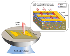
Figure 6. Schematic representation of a photoconductive switch with nano-patterned contacts. The nanometric 'fingers' of the structure allow the plasmonic coupling of laser photons into the semiconductor improving the performance of the device. Figure courtesy of M Jarahi (UCLA).
Download figure:
Standard image High-resolution image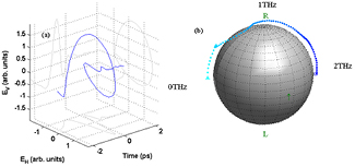
Figure 7. (a) Shows a 3D representation of a terahertz pulse with non-planar polarisation detected by a three-contact photoconductive detector, the pulse was produced by propagating a linearly polarized pulse through a 1.6 mm thick X-cut quartz plate. (b) Shows a parametric plot, as a function of frequency, of the states of polarization of the pulse on the Poincare sphere. The triangle represents the start of the curve at f = 0 THz, and the circle the end at f = 2 THz. The data shown here was obtained with the detector reported in and reproduced from [61]. Castro-Camus E, Lloyd-Hughes J, Fu L, Tan H H, Jagadish C and Johnston M B 2007 Opt. Express 15 7047–57. CC BY 3.0.
Download figure:
Standard image High-resolution imageCurrent and future challenges.
The one most important technological challenge that photoconductive emitters face these days is their cost-effective large scale production viability. Low-temperature GaAs (or InGaAs) is still the most widely used material for photoconductive devices, however its fabrication has two major disadvantages. Firstly, the semiconductor properties are difficult to reproduce, even when grown under the same nominal conditions in the same reactor. Secondly, its growth requires being performed in molecular-beam-epitaxy (MBE) machines, which is an expensive method for large scale production of terahertz devices.
Although some approaches like the incorporation of nanometric gaps could improve significantly the performance of photoconductive detectors and eliminate the need for short-carrier-lifetime materials, their large scale production also requires very high resolution fabrication techniques such as electron beam lithography, which is also unlikely to be implemented for large scales cost-effectively.
The development of compact and on-chip THz spectroscopy systems [62], which promise to expand THz spectroscopy into new applications, will be a driver for the further development of photoconductive THz devices. There will be a continued drive for more compact femtosecond lasers system and THz sources which in turn will stimulate the development of THz devices optimised for these systems.
Other future applications of THz-TDS in materials analysis and structural biology will require further advances in polarisation resolving THz detectors (see sections 11 and 13). The challenge here is to develop detectors with good enough polarisation sensitivity to be used in vibrational circular dichroism spectrometers [63].
Advances in science and technology to meet challenges.
On the material front, ion-implanted [64], nanoscale [58], and nanostructured [56] semiconductors are showing promising results for replacing low-temperature grown materials, and the quality of materials grown by chemical-vapor-deposition, atomic-layer-deposition and other techniques, more economical than MBE, is improving.
While advances in device and antenna design have been demonstrated using techniques such as electron beam lithography [59], improvements are needed in high-throughput fabrication techniques. Although the use of extreme-UV photolithography is still relatively restricted to complex microcircuit production, this kind of technology is capable of mass production of devices with features in the scale of ~10 nm, which would be ideal for the fabrication of some of structures such as plasmonic nanostructures.
Concluding remarks.
Terahertz photoconductive devices have evolved dramatically since their introduction in the 1980s. The bandwidth, power and reliability of these devices improved with the use of novel semiconductor materials and contact structures. The viability of fabricating these devices at industrial scales is an issue still being addressed, but promising solutions can be foreseen in the years to come.
6. Components for terahertz imaging
D R S Cumming1, F Simoens2, I Escorcia-Carranza1 and J Grant1
1 Microsystems Technology Group, School of Engineering, University of Glasgow G12 8LT, UK
2 CEA-Leti MINATEC, 17 rue des Martyrs, Grenoble, Cedex 9 38054, France
E-mail: david.cumming.2@glasgow.ac.uk
Status.
Terahertz imaging has been demonstrated using a wide range of methods. These include pulsed time-domain (PTD) and continuous wave (CW) technologies, single detector scanned systems, arrays and focal plane arrays (FPAs). As described in the Friis equation, the overall performance of an imager is determined by its optical properties including source power, system losses, and detector sensitivity. Whatever the means of implementation, all systems rely on the brightness of the illumination source deployed and the responsivity of the detector.
Time-domain systems (as described in section 8) rely on high-speed rectification of a short pulse using either a photoconductive switch or a crystal such as ZnSe. They have a commensurately high frequency bandwidth in the terahertz spectrum, but typically illumination power is weak, a problem that is overcome by using synchronous detection (see section 5). A valuable attribute of these systems is that they provide depth ranging and the potential for spectroscopy. Owing to the low brightness of the sources, image acquisition times are typically quite slow.
Scalar systems are simpler to construct and are only achievable with relatively high power sources. For frequencies of approximately 1 THz and below, CW sources derived from microwave electronics such as Gunn oscillators, backward wave oscillators and diode-multiplied sources can be used. At longer wavelengths, CW sources include large methanol vapour lasers. Quantum cascade lasers are excellent in the mid-IR but for terahertz require cooling and pulsed mode operation, as discussed in section 1. Table 1 and figure 8 summarise the performance of source technologies and the trend over time towards enhanced performance.
Table 1. Terahertz sources.
| Source | Classification | Frequency (THz) | Operation temp | Typical power output | Year | Commercial | Ref. |
|---|---|---|---|---|---|---|---|
| Mercury | Thermal | Broadband | Room | ~10s µWs | 1950s | Bruker, Sciencetch | |
| SiC globar | Thermal | Broadband | Room | µWs | <1950s | ||
| Cosmic background | Thermal | Broadband | Room | ||||
| BWO | Vacuum electronic | 0.65 | Room | 50 mW |
2008 | No | [65] |
| 0.1 | Room | 1.56 mW |
2013 | No | |||
| 0.2 | Room | 10 kW |
2015 | No | |||
| 4.56 mW |
|||||||
| 20 W |
|||||||
| 30 mW |
|||||||
| Free electron lasers | Vacuum electronic | 0.1–4.8 | Room | 5 kW |
2001 | No | [66] |
| 1.28–2.73 | Room | 20 W |
2007 | No | |||
| 500 kW |
|||||||
| 500 W |
|||||||
| Gunn diodes | Solid state electronic | 0.1 | Room | 50 µW |
2007 | No | [67] |
| 0.3 | Room | 23 µW |
2014 | No | |||
| Frequency multiplication devices | Solid state electronic | 0.7–1.1 | Room | 0.625 mW |
2016 | Virginia Diodes | [68] |
| 0.1–0.17 | Room | 16 mW |
2016 | ||||
| Gas | Lasers | 0.5–5 (discrete) | Room | Up to 150 mW | 1970s | Edinburgh Instruments, Coherent | [69] |
| Quantum cascade | Lasers | 4.4 | 8 K | 2 mW |
2002 | No | [70] |
| 4.4 | 10 K | 0.02 mW |
2006 | No | [71] | ||
| 3.4 | 10 K |
|
2014 | No | [72] | ||
| 3.4 | 77 K | 2014 | No | [73] | |||
| 3 | 178 K | 2008 | No | [74] | |||
| 3.15 | 129 K | 2014 | No | ||||
| 3 | 225 K | 2009 | No | ||||
| Difference frequency generation using 2 MIR QCLs | Lasers | 5 | Room | 80 nW |
2007 | No | [75] |
| 3.5 | Room | 1 nW+ | 2015 | No | |||
| 1.9 mW | |||||||
| 100 mW) | |||||||
| 200 nW+ |

Figure 8. Progress of terahertz sources over recent years: BWO = backward wave oscillator ( ), FEL = free electron laser (
 ), FMD = frequency multiplier devices (
 ), gunn diodes (
 ), QCL = quantum cascade laser (at 10 K unless otherwise stated) (
 ), DFG = difference frequency generation (
 ). All data are at room temperature unless otherwise stated.
Download figure:
Standard image High-resolution imageDetector technologies are improving in terms of noise equivalent power (NEP), responsivity (Rv) and potential for integration, e.g. into focal plane arrays. Table 2 and figure 9 show representative data for a range of detector technologies at room temperature, and progress over recent years. Several of the detectors have been designed specifically for use in imaging applications and we have specified array size and electronically achievable frame rate where relevant. Note that noise limitations and low source power means that these rates are not always achieved in practice.
Table 2. Terahertz detectors.
| Detector | Freq. (THz) | Rv (V W−1) | NEP | Frame rate/response time | FPA size | Year | Commercial | Ref. |
|---|---|---|---|---|---|---|---|---|
| Schottky barrier diode (SBD) |
|
|
|
|
 Single detector Single detector |
2007 | VDI | |
| SBD | 0.86 | 273 | 42 |
−1 µs |
 Single detector 4 × 4 Single detector 4 × 4  |
2013 | — | [76] |
| 0.28 | 336 | 290 pW |
||||||
| Photo conductive | 0.1–4.0 | — | — | — | Single detector | 2011 | EKSPLA | |
| 1985 | ||||||||
| Folded dipole antenna | 0.6–1.0 | 800 (1.027 THz) | 66 |
— |  Single detector Single detector |
2011 | STM | |
|
0.7–1.1 | 115 × 103 (0.856 THz) | 12 nW |
25 Hz |
32 × 32  |
2012 | STM | |
| VOx micro-bolometer | 2.5 |
|
|
|
 Single detector 5 × 5 Single detector 5 × 5  |
|
|
|
| 2.5 | ||||||||
| Bolometer | 4.25 | — | 24.7 pW |
50 Hz |
384 × 288  |
2013 | INO | |
| 2.54 | — | 76.4 pW |
||||||
| Golay cells | 0.2–20 | 10 × 103 (12.5 Hz modulation) | 10 × 103 |
25 ms |
 Single detector Single detector |
2009 | Microtech | |
| Micro- bolometer | 1.0–7.0 | — | <100 pW |
30 Hz |
320 × 240  |
2014 | NEC | |
| LiTaO3 | 0.1–300 | — | 96 nW |
50 Hz |
320 × 320  |
2014 | Ophir Photonics | |
| Pyroelectric | ||||||||
| Pyroelectric | 0.3, 1.0, 3.010 | 18.3 × 10³ (10 Hz mod.) | 440 |
10 Hz |
 Single detector Single detector |
2009 | QMC | |
| Hot electron | 0.89 | 0.095 | 7.4 × 10³ |
200 Hz |
 Single detector Single detector |
2007 | — | [79] |
| Bolometer | ||||||||
| SixGey:H micro- bolometer | 0.934 | 170 | 200 |
1 ms |
 Single detector Single detector |
2010 | — | [80] |
| α-Si micro-bolometer | 2.4 | 14 × 106 | 30 pW |
— | 320 × 240  |
2011 | CEA-Leti | [81] |
| 5.9 × 10⁶ | 68 pW |
|||||||
| Nb5N6 micro-bolometer | 0.1 | 100.5 | 398 |
1 KHz |
 Single detector Single detector |
2008 | — | [82] |
| Vox micro-bolometer | 2.8 | 200 × 103 | 35 pW |
30 Hz |
160 × 120  |
2008 | Infrared Systems | |
| Antenna QW cavity | 2.0–4.0 | 12.6 × 10 (2.5 THz) | 32 pW |
25 Hz |
320 × 240  |
2014 | CEA-Leti | [83] |
| VOx micro-bolometer | 3.1 | — | 280 pW |
16 ms |
640 × 480  |
2008 | NEC | |
| Folded dipole antenna | 0.65 | 1.1 × 10³ (0.15 V bias) | 50 |
— |  Single detector Single detector |
2010 | STM | |
| FET | 0.2–4.3 | 528 (1.4 THz) | 28 |
— |  Single detector Single detector |
2012 | — | [84] |
aAchieved imaging frame rate. bResponse time of individual sensor or pixel. cNEP for arrays operating in video modes. dNEP for single detectors (pW (√Hz)−1).
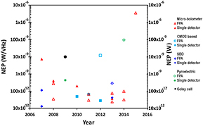
Figure 9. Progress of terahertz detectors over recent years: micro-bolometer based FPA ( ), micro-bolometer single detector (
 ), CMOS based FPA (
 ), CMOS based single detector (
 ), SBD FPA (
 ), SBD single detector (
 ), pyroelectric FPA (
 ), pyroelectric single detector (
 ) and Golay cell (
 ). NEP for single detectors is on the left axis (closed symbols) and NEP for arrays is on the right axis (open symbols).
Download figure:
Standard image High-resolution imageCurrent and future challenges.
Many application areas have emerged for terahertz imaging, and this has motivated a great deal of research in the underpinning technology. The breadth and societal value of the applications is very great, and are briefly summarised as follows:
- Stand-off detection of hidden objects and weapons
- Non-invasive medical and dental diagnostics
- Detection of cracks and defects in materials e.g. solar panels, plastics
- Non-destructive rapid fault isolation in IC packages
- Drug discovery and formulation analysis of coatings and cores
- Non-contact imaging for conservation of paintings, manuscripts and artefacts
- Monitoring of crop and plant hydration levels
The challenge for imaging system developers is to devise miniature systems suitable for use in the field. These may be handheld devices or, for example, units for use on remotely operated vehicles (ROVs). It will therefore be necessary to produce high power, low cost and small source technologies that do not require cryogenic cooling. Similarly, there will be a requirement for uncooled detectors. Since, as already noted, full system performance accounts for the attributes of sources, system losses and sensor performance the development of sources and detector technologies will advance in tandem.
Advances in science and technology to meet challenges.
Future expectations for terahertz imaging systems include video rate imaging (at least 25 fps) at VGA resolution. Further into the future, HD format will be the normal expectation for any imaging system. Image resolution (as opposed to display resolution), noise and dynamic range are all expected to improve. These improvements will rely on advancement in source, detector and optical/system design technology. Specifically, compact, room temperature terahertz sources in the region of 10 mW average power are essential in order to enable stand-off imaging at distances greater than 1 m. Such sources when coupled with a Si CMOS FPA would render a low-cost THz camera (we estimate <US$5 K per unit) that could find wide spread use in applications such as stand-off detection of hidden objects and non-invasive medical (e.g. oncology) and dental diagnostics. For synchronous detection, current developments are aimed at decreasing acquisition times by using multi-channel systems and on employing quasi time domain spectroscopy (QTDS) by replacing the costly femtosecond laser with an inexpensive multimode laser diode. There will also be advances in sophisticated imaging modalities including near field imaging for high resolution imaging and confocal imaging that promises depth information using CW scalar imaging technologies.
Concluding remarks.
The development of imaging systems to meet a range of growing applications for terahertz is presently limited by the available technologies, irrespective of the image system configuration and modality. Whether the intended application entails the development of a microscope, a far-field or near-field imager, or the use of scalar or time-domain techniques, there is a demand for improved source and detector technologies. Work is required to improve every attribute including, but not limited to: source power; terahertz bandwidth; operating temperature; responsivity and NEP; and array size where deployed. Improvements in these basic component measures will lead to imaging systems with improved: frame rate; resolution; dynamic range; stand-off distance; and reduced size and weight. As can be seen from the review data presented here it is likely that semiconductor technologies will play a vital role and in particular we highlight potential advances in semiconductor laser sources and CMOS-based detector technologies. There will also be a need for further advances in passive components based on antenna, lens and metamaterial theory, design and implementation.
7. Passive THz components
Stepan Lucyszyn1, Makoto Kuwata-Gonokami2 and Kuniaki Konishi2
1 Department of Electrical and Electronic Engineering, Imperial College London, Exhibition Road, London, SW7 2AZ, UK
2 Department of Physics, University of Tokyo, 7-3-1 Hongo, Bunkyo-ku, Tokyo 113-8656, Japan
Status.
Coherent time-domain spectroscopy and non-coherent frequency-domain radiometry are two examples of ultra-broadband THz applications. In general, where performance is paramount, quasi-optical front-end implementations are preferred over the use of guided-wave structures because of the need to minimizing material loss contributions. However, the relentless advancements in achieving ever-higher performance sources and detectors are beginning to relax the requirements for passive components in the lower region of the cost-performance application space. Moreover, with the drive to make complete systems smaller, lighter and cheaper, guided-wave structures offer distinct advantages over their quasi-optical counterparts; the former has inherent advantages in terms of providing better isolation, a wider choice of implementation solutions and can be more easily integrated with active devices without the need for optical alignment accuracy. While transmission lines (e.g. microstrip, coplanar waveguide and coplanar strip) represent the obvious solutions for realizing passives on hybrid and monolithic millimetre-wave integrated circuits, in general, they can suffer from high substrate and radiation losses. In addition, their relatively high conduction current densities result in high dissipative (ohmic) losses at terahertz frequencies. As a result, only low quality factor/high attenuation components are possible at room temperature. Usually, to achieve best performance at room temperature, off-chip resonator/filter solutions are needed. Nevertheless, many papers report on the predicted simulated performance of transmission line-based monolithic THz filters; few give measured results. One notable exception is the work by Nagel et al [85]. Here, a 0.61 THz second-order thin-film microstrip coupled-line band-pass filter is demonstrated. With gold metallisation and benzocyclobutene dielectric layers, on a silicon substrate having an integrated photoconductive switch, the filter exhibits a measured loaded quality factor of ~10 and insertion loss of −11 dB [85].
Surface plasmon waveguides suffer from relatively poor mode conversion efficiency and high attenuation due to ohmic losses. Nevertheless, because of their tight field confinement, near-field enhancement characteristics and ability to overcome diffraction limits, devices based on the surface plasmon polariton (SPP) offer the potential for future SPP-based integrated circuits at THz frequencies.
Three examples of high-performance guided-wave technologies used at terahertz frequencies are considered; (1) all metal, (2) metal-dielectric and (3) all dielectric. In general, since dielectric losses can be much lower than those associated with normal room-temperature conductors, lower loss/high quality factor passives can be realized by minimizing conduction current densities and ideally avoiding the use of metals altogether. All three relatively low loss waveguide technologies have been used to demonstrate key components (e.g. power couplers and resonators, used in high performance impedance matching networks, filters and antennas). (1) Metal-pipe waveguides have historically been around for over a century. However, it is only since 2016 that international standards were agreed for operating above 0.1 THz; the IEEE P1785 Working Group proposed standards up to 5 THz [86]. This recognises the growing importance of this guided-wave medium for industrial applications. Monolithic forms of hollow (air-filled) metal-pipe rectangular waveguide technologies have been around since the early 1990s, first introduced by JPL/Caltech for silicon integration with active devices. Since then there has been a raft of technologies that have moved ever higher in frequency and/or with lower manufacturing costs. Without introducing additional functionality but still maintaining high performance, the University of Birmingham (UK) is currently replacing expensive bulk micromachining of silicon by surface micromachining of SU-8 photoresist sacrificial building materials, recently demonstrating split-block waveguides from 0.5 to 0.75 THz, with integrated 3rd order band-pass filters. This idea follows on from a similar 'snap-together' technology introduced by the UK's EPSRC-funded Terahertz Integrated Technology Initiative (TINTIN) research programme (a collaboration between the Universities of Bath, Reading, Nottingham and Leeds). In 2006, TINTIN demonstrated slotted H-plane sectoral horn antennas at 1.6 THz. (2) Oversized dielectric-lined metal-pipe rectangular and circular waveguides operating with a quasi-single mode of propagation were first introduced in 1963 and subsequently demonstrated losses as low as 0.0037 dB m−1 at 150 GHz with ~10 wavelength diameter structures lined with a low-loss dielectric and below 1 dB m−1 above ca. 0.3 THz with ~20 wavelength diameter structures lined with a high-loss dielectric. More recently, a silver-coated PTFE (Teflon™) circular waveguide has been demonstrated, having a measured transmission loss of ~20 dB m−1 across the ca. 1.0–1.6 THz frequency range [87]. (3) Rectangular dielectric waveguide components avoid skin-effect related losses altogether, but still suffer from poor isolation. To improve field confinement, photonic crystal waveguides exploit Bragg reflections at the boundaries of dielectric waveguides. An example of a bendable Topas polymer photonic crystal fibre was reported by Nielsen et al, having a loss of <10 dB m−1 at 0.6 THz [88]; while an photonic crystal resonator that can potentially combine electric field sensing with integrated electronics has been demonstrated in high-resistivity silicon [89].
Conventional optical components can be used in the THz frequency region. Unfortunately, the performances of THz quasi-optics have not reached the same levels as found at the much shorter optical wavelengths, while associated costs are generally considered higher. As a result, a significant improvement and further development is still needed for ultra-broadband THz applications. For example, a polarizer is an essential component found on many quasi-optical benches and breadboards. High extinction ratio and broadband performance are required. The wire grid polarizer is currently the most popular solution at THz frequencies, but their extinction ratio is inferior and they are more expensive than those in the optical region. Recently, new THz polarizers have been developed using exotic materials such as liquid crystals and carbon nanotubes offering extinction ratios as high as 50 dB, which is comparable to those at shorter wavelengths [90]. Wave plates represent another important component for polarization control. The quartz crystal is commonly used because it is transparent and has birefringence in the THz frequency region. However, crystal wave plates only work at a single frequency. Recently, Nagai et al proposed and demonstrated a new scheme to realize broadband wave plates, which works from 2.0 to 3.1 THz by utilizing a stacked waveguide structure [91]. Filters are indispensable components in spectroscopy. Metal mesh filters have been used for a long time at millimetre-wave frequencies, but have recently extending into the sub-millimetre-wave (i.e. THz) region and is considered a class of metamaterials or metasurfaces [92].
Current and future challenges.
Existing guided-wave structures and quasi-optical component technologies can achieve reasonable performance at terahertz frequencies, in terms of field confinement, transmission loss and frequency dispersion, over a broad spectral range. However, even with high-end applications, size, mass and cost may still pose serious challenges. Moreover, for ubiquitous applications, the cost of achieving even moderate performance must be addressed in its passive components and associated subsystems. This becomes even harder to address when component tuneability and subsystem reconfigureability (found at microwave and millimetre-wave frequencies) is required in future multifunctional systems.
Advances in science and technology to meet challenges.
In the lower region of the cost-performance application space, with voxel sizes heading towards 10 microns, additive manufacturing technologies that include 3D printing (e.g. 3D printed plastic structures with optional gold-copper surface deposition) are moving into the terahertz band. In the upper region of the performance-cost application space, traditional micromachining and microelectromechanical systems (MEMS) technologies can increase performance and provide additional functionality, respectively. Tuneable terahertz components would otherwise be difficult to realize within an integrated environment, as the introduction of mechanical tuning mechanisms generally increases both losses and the size of the overall subsystem. Sandia National Laboratories in the U.S. recently reported a 3 THz meandered metal-pipe rectangular waveguide with H-plane horn antenna coupling, manufactured using conventional surface micromachining [93]. A scanning electron micrograph of this structure is shown in figure 10. With electroplated gold walls, the measured transmission loss is approximately 1.3 ± 0.1 dB mm−1 or 0.12 dB/wavelength at 3.1 THz.
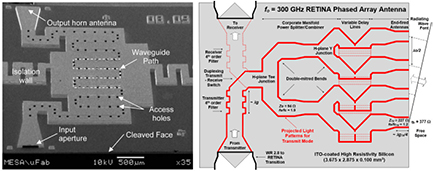
Figure 10. Left: surface micromachined integrated 3 THz meandered metal-pipe rectangular waveguide with H-plane horn antenna coupling [93]. Right: concept illustration of a 0.3 THz 'virtual' substrate integrated waveguide tuneable and reconfigureable phased array antenna subsystem using RETINA technology. Reproduced from [94]. Image stated to be in the public domain. © 2011 IEEE. Reprinted, with permission, from [93].
Download figure:
Standard image High-resolution imageIn order to meet future challenges of providing integrated tuneable components and reconfigureable subsystems, without the use of either conventional electronic or (micro)mechanical switches, which can be cumbersome at THz frequencies, a solution was proposed by Imperial College London in the UK [94]. Known as a reconfigureable terahertz integrated architecture (RETINA), metal-pipe rectangular waveguide having pseudo-conducting (plasma) sidewalls are generated within high-resistivity silicon wafers, patterned by programmable laser or LED light sources. A concept illustration of how a RETINA phased array antenna can incorporate transmit-receive duplexer switching and tuneable time steering, by simply changing the pattern of light, is shown in figure 10.
Alternatively, in order to develop practical THz quasi-optics, 'tuneable metamaterials' have the potential to be an effective solution. Metamaterials are artificial structures that can be engineered for the arbitral control of THz waves. Unlike at optical wavelengths, good conductors have lower losses at THz frequencies. As a result, the basic concept of the metal mesh filter can be expanded to other forms of metamaterials that can be used to implement high-performance THz quasi-optics. Moreover, both MEMS and photoexcitation technologies may have a future role to play in realizing tuneable metamaterial properties [95]. With the former, the size of MEMS can be made comparable to the free space wavelength and so the active control of metamaterial is not only possible but has already been demonstrated at THz frequencies. For example, the University of Tokyo in Japan demonstrated handedness-switching of chirality with a ca. 1 THz metamaterial, shown in figure 11, which can be used to realize an active THz polarization modulator [96]. With the latter, within a semiconductor, photo-induced carriers can introduce individual defects within a metamaterial or even generate a complete 2D 'virtual' metamaterial, which can be controlled by changing the light source patterns.

Figure 11. MEMS spirals [96] (a): microphotograph in the pre-actuation state, (b) microphotograph in the on-actuation state, and (c) illustration of THz polarization modulator operation. Images reprinted by permission from Macmillan Publishers Ltd: NATURE COMMUNICATIONS [96], Copyright (2015).
Download figure:
Standard image High-resolution imageConcluding remarks.
With the relentless advances in the performance of active devices and circuits that make up sources, amplifiers, active modulators and detectors, the associated passive components (implemented with either guided-wave structures or free-space quasi-optics) will ultimately limit the overall performance of front-end THz subsystems. Existing and emerging passive component technologies, used to perform vital functions (e.g. within impedance/amplitude/phase matching networks, power couplers, filters, antennas, polarizers and even switches), must find their niche location(s) within the ever-expanding cost-performance application space. Be-spoke passive solutions will be needed to keep pace with developments in active technologies, ideally without the need for cryogenic cooling.
8. Developments in THz time domain spectroscopy
Martin Koch
Faculty of Physics and Material Sciences Center, Philipps-Universität Marburg, Marburg D-35032, Germany
Status.
In the past it was very cumbersome to access the terahertz frequency range experimentally. This changed with the advent of terahertz time-domain spectroscopy which was first demonstrated in 1988 by Smith and coworkers [97]. They used a colliding pulse mode-locked (CPM) dye laser which gated photoconductive antennas on the basis of radiation damaged silicon-on-sapphire (SOS). In 1990 Grischkowsky and coworkers demonstrated that this technique allows for high-quality spectroscopy in the lower terahertz range [98]. In the early 1990s mode-locked titanium sapphire became available. Since they are much easier to operate and offer a higher stability they immediately replaced the CPM lasers as driving source for the antennas. Soon also the SOS antennas were replaced by structures based on low-temperature grown GaAs. Figure 12 shows a schematic diagram of a typical free-space spectrometer at this time.
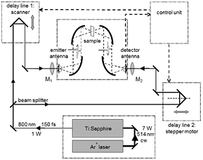
Figure 12. Schematic diagram of a free-space THz time-domain spectrometer. The emission from a titanium sapphire laser, which is pumped by an argon ion laser is used to drive photoconductive dipole antennas. The emitted THz pulses are guided by off-axis parabolic mirrors. Taken from [103] with permission from Springer (Copyright 2011) which contains a more detailed description of the system.
Download figure:
Standard image High-resolution imageNuss and coworkers were the first to further develop this photoconducting antenna emitter-receiver scheme to the point where 2D images of objects a few centimeters in diameter could be accumulated [99]. Since this first demonstration in 1995, more advanced imaging schemes such as THz tomography, and THz near-field, dark-field and single-pixel imaging have been explored (see [100] for a review).
At this time all terahertz-time-domain spectrometers were free-space spectrometers i.e. the laser beams were guided in air towards the antennas. Hence, moving one antenna to perform angle dependent experiments was cumbersome. In 2000 Picometrix introduced fibre-coupled THz systems [101], which allows us to freely move THz antennas and therefore provide flexibility and also stability. In 2007 Wilk et al presented a further advancement [102]. They demonstrated a THz TDS system based on a cost-effective fibre laser operation at 1.55 µm. These lasers are based on low-cost telecom components developed for long-term operation. As antenna material low-temperature grown InGaAs/InAlAs multiple-quantum wells were used. On the basis of this technology a variety of different companies today offer fibre-coupled THz TDS systems with a good signal to noise ratio and a reasonable bandwidth. Consequently, these systems are presently making their first steps towards real world applications and into industrial environments.
Current and future challenges.
Although there has been tremendous progress over the past 25 years, THz TDS systems still need to become faster, smaller, more rugged and less expensive. This would be important for industrial applications, for example for the in-line monitoring of goods during the production process. Companies are willing to pay several thousand Euros for a sensor system but not tens of thousands of Euros, which is the present price level. However, system prices of several thousand Euros would still not impose a mass market. For a real mass market the ideal system would need to cost only a few Euros, would have to have the size of a smart phone, would have to acquire thousands of spectra per second with a bandwidth of many THz and would have to still work after being smashed against a wall. At the moment this is asking too much.
Yet, much progress on achieving these goals has been made in the last 10 years—but not simultaneously concerning all aspects. Regarding the measurement speed, significant progress has been made via new mechanical delay lines, some of which are based on fibre-stretchers. New schemes like asynchronous optical sampling (ASOPS), electronically controlled optical sampling (ECOPS), or optical sampling by laser cavity tuning (OSCAT) (see [104] for a comparative discussion) allow for the acquisition of THz waveforms without the use of an external delay line, though ASOPS and ECOPS require the use of two femtosecond lasers which enhances and not lowers the price level of a THz TDS system. Also small and portable THz systems have been demonstrated having the size of a laptop computer. Nevertheless, it remains a challenge to develop low-cost, fast THz systems, which reliably work in rough environments and over a large temperature range.
In addition, imaging systems based on time-domain spectrometers still need to become much faster. Recently, fast imaging systems which use galvanoscanners for deflecting the beam in a raster pattern have been demonstrated. Yet, these systems are far from capturing images at video speed. Faster is an imaging technique, which transforms broadband frequency information of the THz pulses into spatial resolution [105]. It holds the potential to improve the acquisition speed of images by up to two orders of magnitude, but at the price of a reduced spectral information.
Advances in science and technology to meet challenges.
In order to realize the vision above of an ideal mass market system still several years of development are needed. All system components need to drop in price without a reduction in performance. Femtosecond fibre-lasers could be replaced by mode-locked edge emitting and fibre-coupled semiconductor lasers. Potentially, the repetition rate of these lasers can be tuned all-electronically. This would allow for OSCAT based THz spectroscopy systems which employs only one laser and operates without any mechanical delay stage.
Furthermore, there might still be potential to improve the performance of photoconductive antennas—despite the fact that significant progress has already been made regarding antenna structures and materials. The goal material-wise is a structure with very short carrier lifetime and simultaneously high-carrier mobility. This could potentially be achieved by further optimization of quantum film structures. Besides, the cost-level of fibre-coupled antenna need to become lower, which could be achieved by mass-production. This would allow for parallelization of THz channels, which would improve the imaging speed maintaining full spectral and in-depth information.
Finally, passive quasi-optical components need be drop in price. Recently devices produced by compression moulding [106] and by 3D printing [107] have been demonstrated. In particular 3D printing is presently making rapid advances and holds the potential not only to produce THz optics but also spectrometer housings.
Concluding remarks.
Despite the fact that THz time-domain spectroscopy has become a mature field and the technique is used in hundreds of research labs worldwide, there is still significant room for improvement of THz systems. The key could be the further development of mode-locked edge emitting semiconductor lasers and improved photoconductive semiconductor quantum structures. Furthermore, mass production and modern fabrication techniques like 3D printing will have an impact.
9. Terahertz spectroscopy of semiconductors and semiconductor nanostructures
Charles A Schmuttenmaer
Department of Chemistry, Yale University, 225 Prospect Street, P.O. Box 208107, New Haven, Connecticut 06520-8107, USA
Status.
Laser-based terahertz (THz) time-domain spectroscopy emerged about 25 years ago, and it has proven to be particularly valuable in the characterization of semiconductors and semiconductor nanostructures. In fact, it is now the method of choice for measuring ultrafast time-dependent photoconductivity. This is because it is a non-contact electrical probe with sub-picosecond temporal resolution. Initial studies were not time-resolved, and static, equilibrium properties of semiconductors were measured [98]. However, there was a turning point in year 2000 when Beard et al published a report on transient photoconductivity in bulk GaAs [108]. They outlined many experimental considerations that must be taken into account when making THz measurements to determine electrical properties in a non-contact fashion on a sub-picosecond timescale. Then, in 2002 they showed that it was applicable to nanomaterials such as CdSe quantum dots and dye-sensitized TiO2 nanoparticles [109, 110].
The THz amplitude is measured rather than its intensity, which allows the frequency-dependent complex-valued transient conductivity to be determined directly. While it is true that the real and imaginary conductivity are related through the Kramers-Kronig relations, that analysis assumes that one of the components, either real or imaginary, is known over the frequency range from dc to infinity in order to determine the other component. It is very important that both real and imaginary frequency-dependent conductivities are measured in order to fully characterize the material.
One of the most impressive studies utilizing time-resolved THz spectroscopy to characterize the onset of Coulomb screening and plasmon scattering after photogeneration of an electron-hole plasma in GaAs on a 10–100 fs time scale (see figure 13) [111].

Figure 13. Imaginary (a) and real (b) parts of the inverse dielectric function of GaAs upon photoexcitation. It is seen that the transition from independent electrons and holes to an ensemble of screened quasiparticles occurs on a time scale of 10–100 fs. Reproduced with permission from [111], copyright 2001, Nature Publishing Group.
Download figure:
Standard image High-resolution imageIn addition to using THz pulses as a probe, it is also possible to obtain information on semiconductors and semiconductor nanostructures via THz emission spectroscopy [112, 113]. In this case, the carrier dynamics upon photoexcitation are imprinted on the emitted THz pulse. While not used as widely as TRTS, it offers several advantages such as a spatial resolution that is determined by the visible or near IR excitation beam, and not the long wavelength THz beam.
Current and future challenges.
Both experimental and theoretical challenges lie ahead. On the experimental side, improvements in sensitivity, bandwidth, spatial resolution, and THz field strength are needed. On the theoretical side, more exploration is required.
Single particle studies.
There have been optical studies of single particles and single molecules for well over two decades. It has been possible to carry out similar studies in the THz region when employing a metal tip or something related [114, 115]. However, it would be beneficial to have high enough sensitivity such that THz studies of single semiconductor nanoparticles could be carried out. This would allow one to probe carrier dynamics within single particles rather than looking at the ensemble average as is currently done.
Broadband studies.
More information is always better than less information. Extending the bandwidth of THz sources while maintaining an excellent signal to noise ratio (SNR) is a key challenge. There have been a number of developments over the last 10 or more years in which truly impressive bandwidth is achieved (up to 100 THz) [111, 116]. On the other hand, the overall dynamic range suffers because the power is spread over a much larger region. Therefore, it becomes difficult to carry out spectroscopic studies, especially on weakly absorbing samples.
Spatial resolution.
Spatial resolution is quite important when probing nanomaterials and nanostructures. The diffraction limit for a THz pulse is on the order of 300 microns. It might not be possible to dilute the sample such that there is only one particle within a desired area or volume. Therefore, we need to find ways to probe semiconductors and semiconductor nanostructures on extreme sub-wavelength scales. Section 10, which looks at THz microscopy provides detailed analysis of the current and future challenges in this area [117].
Nonlinear studies.
The optical community benefitted tremendously from ultrafast/nonlinear studies. Transient absorption, three wave mixing, four wave mixing, induced transparency, 2D experiments, etc. This is an area where THz needs to go. We already have optical pump/THz probe, so we need to move toward THz pump/THz probe. There already is movement in this direction.
Theory.
There has been considerable discussion in the literature regarding the most appropriate model to use when analyzing transient photoconductivity data. It is worth emphasizing that THz spectroscopic measurements determine the frequency-dependent complex conductivity without assuming any model whatsoever. However, it is useful to invoke a model in order to understand the underlying reasons for the frequency-dependent conductivity. That is, to characterize the scattering time and carrier density rather than simply looking at a plot of frequency-dependent real and imaginary conductivity. Ultimately, full-fledged theories of conductivity should be utilized rather than phenomenological models.
Advances in science and technology to meet challenges.
Some advances required to meet these challenges are already underway, but others are more speculative.
Single particle studies.
Hegmann et al have probed single InAs nanodots by using an STM tip [115]. However, it would be advantages in characterizing dispersed individual particles without a probe tip. The advances required are that the SNR be improved by six to eight orders of magnitude (at the power level, which corresponds to only three to four orders of magnitude at the amplitude level) in order to measure the transient photoconductivity in a 10 nm diameter GaAs nanoparticle. This is achievable if the THz pulse amplitude is increased while simultaneously decreasing the noise level. In fact, decreasing the noise level may well be more fruitful since it is already somewhat common to generate THz field amplitudes of 1 MV cm−1 or greater. In fact, the overall absorption process is perturbed at high field strengths, so therefore, it is necessary to reduce the noise levels. There is a great deal of literature on low noise THz detectors, but it is not directly applicable to pulsed THz studies. In particular the development of single photon THz detectors would be particularly important.
Broadband studies.
As mentioned above, extremely broadband THz sources already exist, but they are somewhat complicated compared to standard optical rectification and photoconductive antennas. There are three challenges that need to be solved: 1. Make them easier to implement, 2. Increase the THz amplitude such that it is possible to carry out high sensitivity spectroscopic studies when the power is spread across the spectrum from 0.1 to 30 THz, and 3. Decrease the noise level.
Spatial resolution.
The diffraction limit is the diffraction limit. There are existing techniques for probing smaller areas under specific conditions. One possibility is to employ THz emission spectroscopy rather than the more common THz absorption spectroscopy. As seen in figure 14, it is possible to map out carrier dynamics with roughly 1 micron resolution. It has been shown that focusing the THz beam on a sharp metal tip can provide resolution of roughly 1 micron [114, 115], and many exciting improvements and developments are discussed in Section 10 of this roadmap [117]. Finally, it might be possible to exceed the diffraction limit using a superlens based on THz metamaterials.

Figure 14. Amplitude of THz emission from photoexcitation of an integrated circuit with 1 micron spatial resolution. Part (a) shows an undamaged chip, part (b) illustrates that the defect created by severing the ground line using fast ion beam etching can be readily identified (shown in the CAD drawing in part (c)). Reproduced with permission from [112], copyright 2011, Optical Society of America.
Download figure:
Standard image High-resolution imageNonlinear studies.
This will require more intense THz pulses. Quite a bit of progress has already been made in this direction. For table-top systems, one possibility is to focus the first and second harmonic of the amplified NIR laser and the air plasma that is generated produces a THz pulse [116]. Another is tilted wavefront generation in lithium niobate [25] where maximum field strengths greater than 1 MV cm−1 have been achieved.
Theory.
One challenge to be overcome is attaining consensus on which phenomenological model is best and most appropriate for nanostructured semiconductors. This will require very high quality data that covers from 0.1 to 20 THz such that the model that best fits the data will be unambiguous. Advances in computer hardware will allow more rigorous theories and more extensive simulations to be applied routinely. The other required advance is that more theoreticians focus their attention on these systems.
Concluding remarks.
Terahertz spectroscopy, both static and time-resolved, will continue to be a leading method for characterization of semiconductors and semiconductor nanostructures. In the future, it will be used to probe increasingly smaller regions and will also be used to drive systems out of equilibrium. One can also envision using photoexcited semiconductors as transient optical components such tunable filters when coupled with metamaterials.
10. THz microscopy
Tyler L Cocker and Rupert Huber
Institut für Experimentelle und Angewandte Physik, Universität Regensburg, Universitätsstraße 31, 93053 Regensburg, Germany
Status.
The THz frequency range is home to many important low-energy elementary excitations in condensed matter. These include plasmons, phonons, magnons, and correlation-induced energy gaps. Time-resolved THz spectroscopy has proven extremely useful for studying the dynamics of such excitations in nanomaterials, as was described in section 9. Its strengths—sub-cycle time resolution and field-resolved detection—are particularly valuable, as nanosystems can exhibit transient behavior that is both exotic and very fast (lifetime <10 ps). However, THz spectroscopy has a major drawback, namely its limited spatial resolution. Diffraction prevents light of a wavelength λ from being focused to a spot with a diameter smaller than λ/2 (~150 µm for a frequency of 1 THz). THz spectroscopy of nanosystems is therefore restricted to measurements of ensembles. As a result, the complex conductivities extracted from far-field THz spectroscopy are averages over sample heterogeneity and require significant modeling to interpret. More importantly, local effects that depend intrinsically on the size, structure, or shape of individual nanostructures can be obscured completely (figure 15(a)). Terahertz researchers have met this challenge by developing an array of microscopy techniques that extend the scope of THz spectroscopy. These range from approaches based on optical nonlinearities [118, 119] (e.g. THz emission microscopy [118]), where the superior focusing of short-wavelength light is utilized to gain enhanced spatial resolution in the THz range, to scanning probe techniques, where the evanescent fields localized around sub-wavelength structures are used to access nanoscale information [114, 115, 120–125]. For example, fields coupled to a probe can be used to measure local material properties, or alternatively to measure the shapes of the evanescent fields around a subwavelength sample. One of the most popular and versatile options for THz scanning probe experiments is scattering-type near-field scanning THz microscopy [114, 122–125]. Here, a metallic atomic force microscope tip confines THz light to a volume defined by the radius of curvature of the tip apex (figure 15(b)). When a sample is subsequently brought in close proximity to the tip it scatters this evanescent THz field and thereby conveys its local dielectric properties to the far field. Scattering-type near-field microscopy is particularly well established at the high-frequency end of the THz spectrum [123–125]. Nevertheless, advances in THz technology are still driving progress. Recently, ultrabroadband electro-optic sampling with single-coherent-photon sensitivity was combined with near-field microscopy to extend sub-cycle THz spectroscopy to the sub-nanoparticle scale (figure 16) [125]. Electro-optic sampling measures the absolute phase of scattered waves, and therefore provides prospective access to local wave packets in the time domain—such as propagating surface plasmons—which cannot be resolved by linear interferometry. Entirely new THz microscopy techniques are also being perfected, such as THz scanning tunneling microscopy (THz-STM). In THz-STM, THz pulses drive a train of subpicosecond current pulses across an STM tunnel junction, enabling ultrafast imaging with record spatial resolution [115]. In the first demonstration of this technique, features on the ~2 nm scale were imaged. Still, there is good reason to believe that even better spatial resolution will soon be achieved by THz-STM, as will be discussed below.

Figure 15. Scattering-type near-field scanning THz microscopy. (a) THz pulses focused onto a sample composed of nanoparticles on a flat substrate are reflected, carrying away information about the effective dielectric function averaged over the THz focal spot. (b) Introducing a sharp metallic tip into the THz focus leads to a strong confinement of the THz field at the tip apex. This evanescent field can be scattered into the far field through interaction with a nanoparticle sample, thereby providing access to the local dielectric function of the nanoparticle with spatial resolution defined by the radius of curvature of the tip apex.
Download figure:
Standard image High-resolution image
Figure 16. Ultrafast, ultrabroadband THz spectroscopy on the sub-nanoparticle scale. (a) Atomic force microscope image of an indium arsenide nanowire on a diamond substrate. (b) Ultrafast near-field THz 'snapshot' images of the nanowire taken before (top) and after (bottom) photoexcitation by a near-infrared pump pulse. (c) Electro-optic near-field waveforms measured at the center of the nanowire [125]. Reprinted by permission from Macmillan Publishers Ltd: NATURE PHOTONICS [125], Copyright (2014).
Download figure:
Standard image High-resolution imageCurrent and future challenges.
We envisage four primary objectives for THz microscopy in the coming years: (i) Improve signal-to-noise ratios to broaden the scope of THz microscopy and resolve subtle nanoscale effects. With increased sensitivity, field-resolved detection of scattered pulses could allow the propagation of plasmonic wavepackets to be observed in the time domain. (ii) Introduce cryogenic operation to study local ordering during material phase transitions. Ultrafast near-field measurements at variable temperatures would be of particular interest. Low sample temperatures would carry the added benefit of bringing THz resonances into focus that are typically washed out at room temperature. (iii) Advance from linear to nonlinear THz near-field spectroscopy. High-field, phase-stable THz pulses confined to the apex of a tip could open up a new world of THz coherent control on the nanoscale. Field-resolved detection of the scattered pulses will be essential, as it will allow researchers to trace the nonlinear, carrier-envelope-phase-dependent material response in the time domain and resolve frequencies outside of the excitation bandwidth. (iv) Take THz imaging to the ultimate length scale. Atomic resolution could herald the start of a new era for THz microscopy—that of ultrafast quantum imaging.
Advances in science and technology to meet challenges.
The primary challenge currently limiting advances in time-resolved scattering-type THz scanning probe microscopy is the relatively small number of THz photons that carry information from the near field to the far field. Increasing the incident THz pulse energy would immediately improve the signal-to-noise ratio of THz near-field microscopy. Next-generation, ultrastable, high-power, high-repetition-rate THz sources would open new avenues, including nonlinear microscopy and spectroscopy of nanoscale condensed matter and biological systems (see section 11). The list of promising candidate technologies currently under development includes mode-locked quantum cascade lasers, which can directly generate phase-stable THz pulses out of their cavities (see section 1). Additionally, refined tip preparation and structuring could increase THz coupling efficiencies. Sufficiently sophisticated tip engineering could even enable polarization control, magnetic field sensitivity, or increased evanescent field confinement, and hence enhanced spatial resolution. Improvements to the spatial resolution and sensitivity of THz near-field microscopy are the first steps towards accessing physics on a new, smaller length scale. However, sample stability and preparation must also be optimized. THz near-field experiments are typically performed in ambient conditions, in contrast to cutting edge atomic force microscopy and scanning tunneling microscopy studies. Dielectric properties on the atomic and molecular scale could ultimately become visible to THz near-field microscopy, but we expect this will only be possible once cryogenic, ultrahigh vacuum operation has been established in conjunction with ultraclean sample preparation. Similarly, the extension to cryogenic conditions would significantly stabilize THz-STM imaging on the smallest length scales. Indeed, the ultimate limits of THz-STM will only be revealed under sufficiently clean experimental conditions.
Concluding remarks.
THz microscopy has recently made the transition from proof-of-concept experiments to an established class of diagnostic techniques with unique capabilities. Subjects range from evanescent fields confined to the surfaces of subwavelength objects to the local material properties of inhomogeneous media and nanoparticles. Future advances in THz generation technology and near-field tip preparation will improve near-field signal-to-noise ratios. This will, in turn, lead to a greater ability to distinguish between small changes in the local dielectric function. Advances in THz generation may ultimately even enable nonlinear THz near-field experiments at the apex of a tip. Meanwhile, cleaner sample conditions could play a key role in improving the spatial resolution of THz microscopy. THz-STM in particular will benefit greatly from ultraclean cryogenic operation under ultrahigh vacuum. It is poised to enter a completely new experimental regime of ultrafast and ultrasmall.
11. Biological applications of THz technology
A G Markelz1 and Z D Taylor2
1 Department of Physics, University at Buffalo, The State University of New York, Buffalo, NY 14620, USA
2 Department of Bioengineering, University of California, Los Angeles, CA 90095, USA
Status.
The application of THz light to biomedical questions is motivated by: (1) strong absorbance by water; (2) predicted resonances in biomolecules; and (3) low possibility of tissue damage by such low energy photons. Research has naturally fallen into two regimes: molecular and systems. Molecular studies use the unique small photon energy excitations that correspond to motions to interrogate biomolecules to provide new information. System studies concern investigating THz imaging of and THz effects on cells and tissues. The two approaches go hand in hand, as the dielectric contrast arises in imaging arises from changes in THz dielectric properties in the tissue because the spatially varying biochemistry associated with disease or tissue damage. We will therefore discuss these two regimes separately. A more thorough and specific discussion on biomedical instrumentation can be found in section 12. Because of space constraints, many important citations could not be included, some of which can be found in recent reviews [126–129].
Water's strong absorption of THz light provides a method to precisely monitor tissue water content. Recent measurements find the frequency dependence and magnitude of the absorption depends on salt, protein, and DNA content. In addition THz water absorption depends on protein structural changes such as ligand binding or denaturing. Thus THz could distinguish healthy tissue from tissue with a disease or injury resulting in modifications in protein structure or salt/protein content in cells. The strong absorption of water arises from librational motions of waters and water clusters. Measurements have focused on examining how solutes disrupt the bonding networks, changing both the distribution of cluster sizes and the time scale of local motions [130–132].
Relatively small biomolecules, such as carbohydrates and pharmaceuticals with ~10–30 atoms have intramolecular vibrations in the mid infrared (MIR). However packaged pharmaceuticals cannot be monitored in the MIR, as the packaging is not transparent. These products use microcrystalline preparations with lattice phonons in the THz range. The lattice vibrations are dependent both on the intermolecular interactions from the crystal order and intramolecular interactions, resulting in spectral lines that are unique for different molecules and for different enantiomers of the same molecule as discussed in section 13 [133, 134].
By contrast, proteins and DNA molecules have typically 1000s of atoms, and thus (unlike the small biomolecules in section 10), proteins have intramolecular vibrations in the THz range. These collective motions are thought to be critical to protein function. The requirement of a critical hydration level to ensure homogeneous samples, results in a large water background to the protein THz absorbance. Bulk water absorption for solution phase measurements can be removed by freezing the sample, however a smooth broad frequency dependent absorption is still observed. The broad absorbance band is due to the large vibrational density of states with many vibrations closely spaced in energy, and the relaxational response of the amino acid side chains and unfrozen waters adjacent to the protein surface. The lack of narrow resonances for unoriented samples prevents use of THz for protein or DNA identification. However, both the absorbance and refractive index change with small ligand binding for proteins and DNA hybridization, and thus THz may be used for biosensing that does not depend on tagging. More recent anisotropic absorption measurements have found narrow resonances to be discussed in section 12.
Current and future challenges.
A challenge for THz identification of microcrystalline substances is the identification of artifacts, removal of scattering background and multicomponent analysis for composite materials. Circular dichroism may provide a means to specifically address scattering background. However there is lack of THz CD instrumentation. Multicomponent analysis will be aided by better modeling of the materials, including density functional calculations of the expected absorbance. There has been some improved agreement by several groups, which enables the identification of the specific molecular/lattice motions corresponding to a resonance. These calculations are not yet sufficiently robust and accessible for routine use for database building.
For biosensing based on net changes in the broad THz absorbance/refractive index with protein ligand binding and DNA hybridization, there need to be real tests with protein solution with an array of test ligands and concentrations to examine the reliability of THz binding detection. Measurements could be single frequency with high signal to noise and dynamic range with available sources and detectors. Ideally these measurements would be done with the simplest optics, such as a single frequency high power source and a THz camera. Comparisons need to be made to current surface plasmon resonance detection. The THz systems used for these tests need to be standardized, such as current commercial systems, with performance specifications for multiple lab comparison.
It has been demonstrated that anisotropic THz absorbance for aligned protein samples addresses in the relaxational background and large vibrational density of states challenges to measuring intramolecular protein vibrations. Using linear dichroism measurements on protein crystals, distinct narrow resonances unique to both the protein and protein binding state have been observed [135]. This is very exciting. Protein crystals provided the fully hydrated and aligned protein samples, but in the future it would be ideal that alignment could be achieved without crystals. The ability to measure the intramolecular vibrations is a necessary tool to resolve the ongoing argument of their role in biological function. The development of more sophisticated polarimetry measurements may lead to sufficient isolation of specific motions that protein identification via terahertz optical resonances can be achieved. The chief ongoing challenge for these measurements is accurate modeling of the anisotropic terahertz absorbance for proteins. In addition the interpretation of the resonant bands will be a challenge, as these consist not of single vibrations, but sets of vibrations with the same polarization dependence.
Advances in science and technology to meet challenges.
Instrumentation has advanced considerably over the last 20 years. Aqueous solution measurements require high dynamic range measurements, often achieved using high power sources. At this time one can attain single frequency high power THz sources, with examples found in section 1. However tunable high power sources are still not available for the bench top.
Polarimetric measurements can enhance unique spectral resonances for possible identification of biomolecules as well as their specific dynamics. Tools for polarization control and detection are limited at this time, in particular the mating of polarimetry with near field measurements necessary for small samples or high resolution. Ideally a system would have polarization modulation at higher frequencies that currently accessible using current methods of mechanical polarizer spinning. Polarization modulation of a broadband source, or of a frequency tunable source would be necessary and ideally incorporated into microscopy systems such as those mentioned in section 10. Photo-controlled metamaterials with polarization control have been demonstrated, but have limited bandwidth and therefore limited utility for spectroscopy. The most promising methods are those that modulate the output polarization of the terahertz generator either by initial pulse shaping or relative phase delay for the mixing pulses, or electrode switching for current transient generation, some of which are discussed in section 5. Efficient methods such as simultaneous measurement of both transmitted polarizations [136]. One of the chief issues with metamaterials development for polarization control is their limited bandwidth [137].
Molecular modeling focused on terahertz dielectric response of biomaterials is one of the chief challenges to progress. There has been considerable advancement for molecular crystals, but water and proteins remain difficult to model and predict/interpret terahertz spectra. The absolute broadband absorbance has been measured for protein solutions as a function of concentration and binding, but only qualitative modeling has been pursued. This could readily be pursued and would be a necessary first step towards identifying the narrow band resonances in the anisotropic THz data for aligned proteins.
Concluding remarks.
Immediately after the development of THz time domain spectroscopy there was a great rush to make startling claims about THz biomedical capabilities, with the unfortunate result that some deeply flawed results were published. These problematic studies have caused skepticism within the biomedical community. This skepticism is compounded with a natural mistrust of technology that is not familiar. This has meant that the necessary communication and collaboration between optical engineers and physicists with biologist and medical doctors has been limited. Nevertheless the collaborations that have formed contribute to an increasing number of THz studies published in primarily biological journals. An international consortia that includes biomedical researchers is needed to define specific targets of inquiry to take the field to the next level.
12. Medical applications
Vincent P Wallace
The University of Western Australia, 35 Stirling Highway, Crawley WA 6009, Australia
Status.
As mentioned in the previous section, medical applications are motivated by the strong absorption of THz radiation by water. It was in the Hu and Nuss paper 20 years ago that they proposed that terahertz time domain imaging could be used in the medical arena due to the sensitivity of terahertz absorption to water content; and that the degree of hydration of tissue could be used as a measure of disease state [99]. Mittleman et al performed some preliminary work on burnt chicken suggesting that terahertz imaging applications in burn diagnostics and wound healing [138]. The first reported work on terahertz imaging and identifying diseased human tissue was by Arnone et al who demonstrated the differentiation of enamel and dentine in thin sections of extracted human premolar and the detection of early caries [139]. The first lab based in vivo measurements on human skin was presented by Cole et al where it was shown that terahertz can detect a change in skin hydration in real time [139]. This led the company TeraView Ltd to develop a portable flatbed system that was situated in a dermatology clinic at Addenbrooke's Hospital in Cambridge, UK. This system was used to image excised sections of basal cell carcinoma (BCC), a type of skin cancer which often has poorly defined margins, making its complete resection complicated and time consuming. Woodward et al showed terahertz imaging revealed strong contrast between normal skin and BCC [140] and the first in vivo measurements of cancer were reported by Wallace et al (see figure 17); suggesting that terahertz could be used to indicate tumour margins prior to surgery [141]. Correlation of terahertz data from colon tissue to histopathological images stained to show angiogenesis-related changes revealed that new blood vessels (angiogenesis), known to be 'leaky,' had more interstitial fluid present, leading to increased absorption of the terahertz signal [142]. Further, although it has been assumed that water content is the dominant contrast mechanism in terahertz imaging, MacPherson's group has shown this not to be the case and that terahertz imaging can distinguish between normal and diseased liver due to differences in absorption not only by water but also the tissue structure [143]. Numerous groups have now demonstrated medical applications in breast cancer, colon cancer, burn imaging, and corneal hydration. The technology behind terahertz time domain imaging hasn't changed much; but engineering efforts have been made to make system more suitable to the clinical environment which, in turn, will enhance acceptance. For example, an intra-operative probe for detection of breast tumour margins during cancer surgery and endoscopy like devices for in vivo cancer screening (see figure 18).
Figure 17. The first in vivo cancer images. Collected using a flatbed reflection, time domain, imaging system (TeraView Ltd, Cambridge, UK). The clinical photo (left) show only surface feature which can be compare with the terahertz image (centre) which is formed by plotting the the peak of the reflected terahertz pulse. The depth image (right) is form by plotting a point further along the reflected pulse, i.e. which penetrates below the surface, which reveals feature not visible to the naked eye.
Download figure:
Standard image High-resolution image
Figure 18. The photo (left) show the prototype intra-operative surgical probe for use during breast cancer surgery. The graph (right) show the classification of breast cancer data collected with the probe where tumour (red) is well separated from normal tissue (blue).
Download figure:
Standard image High-resolution imageCurrent and future challenges.
Two areas where terahertz imaging showed lots of early promise but has not taken off is in dermatology and dentistry and the reasons for both are similar. Time domain systems use ultrafast, femtosecond lasers for both generation and detection of terahertz radiation, and although there are a myriad of lasers from 'conventional' titanium sapphire to fibre based lasers, they remain the most expensive individual component of any system. The laser itself is well above the equipment price point typical for the disciplines of dermatology and dentistry. For clinical acceptance of any new technology the information provided has to be not only of clinical use and unique information, but also provide value for money, i.e. provide healthcare cost savings over current methods. Mass production of devices could drive down the cost as discussed in section 8. The challenges for terahertz medical imaging could be classified into two areas, scientific and technological. The scientific challenge is to provide unique information not available from other numerous imaging techniques available to the clinician; what does the terahertz image tell you about the tissue pathology not evident otherwise. Is this information sufficiently (statistically significant) different to surrounding tissue to provide the levels of sensitivity and specificity required in clinical decision making? To achieve statistical significance and level of efficacy sufficient for acceptance by regulatory bodies like the Food and Drug Administration (FDA) requires large multicentre clinical trials and a significant financial investment. Water absorption limits the depth of tissue that may be imaged using terahertz to a few hundred microns in skin and up to a centimetre is tissue with more fat content like breast. However, 85% of cancers originate in the epithelial tissues that form the external and internal surface structures of the body and it is often cells in these thin layers that become malignant and hence are accessible with suitable technology, e.g. endoscopes. The technological challenge is to provide this information quickly, ideally in real time, in a flexible, low cost medical device. To achieve these requirements even cheaper and compact laser systems are required, fast scanning or alternative pixel array like CMOS cameras. Further consideration is required on how to analyse and present imaging or diagnostic information that is acceptable to the clinical community.
Advances in science and technology to meet challenges.
To help verify that terahertz is providing unique information about tissue pathology the terahertz clinical data collected needs to be understood using mathematical models. Terahertz spectra of tissues with high water content e.g. skin, follow a similar trend as that for pure water but the absorption is not as high. If tissue homogeneity is assumed, the spectra can be modelled using double Debye theory [144]. Tissues with a high adipose (fat) content appear different and do not follow double Debye theory and it needs to be modified by manipulation and adding an extra term [145]. Modelling is further complicated when tissue structure is taken into account and Taylor et al have done this effectively using Bruggeman effective media theory [146]. Further development of these models and fitting to a variety of clinical data, with the addition of inverse modelling to help develop technology will aid better understanding of how terahertz interacts with tissues, which is vital to future development of the technology. Another advance is to enhance terahertz biomedical imaging by introducing exogenous contrast agents, such as gold nanoparticles, which have been shown to improve contrast. Oh and Son found that the terahertz reflection signal increased by 20% in the cancer cells with gold nanoparticles upon their irradiation with an infrared (IR) laser, due to a rise in the temperature of local water [147]. With suitable specific binding proteins placed on the surface of the nanoparticles they could be preferentially taken up by cancers in vivo and with a suitable excitation and imaging set-up this could lead to improved differentiation between tumour and normal tissues using terahertz.
The greatest contrast seen with time domain systems, for example, between cancer and normal tissue occurs below 1 THz and peaks around 500 GHz [148], hence a time-domain system an expensive ultrafast laser may not be required for medical applications. Taylor et al have used a 525 GHz reflection imaging system to image full and partial thickness burns in an in vivo animal model which showed different regions of the wound [149]. Further work is needed to confirm these findings. There are continual developments in the field of quantum cascade lasers (QCLs) described in detail in section 1. One exciting development is Terahertz imaging through self-mixing in a QCL [150] and this is now being investigated as a method to image biological samples. Despite there still being the need for cryogenic cooling this technique may well overcome some of the technical challenges faced using time domain systems.
Concluding remarks.
There remains are a number of potential advantages in the application of terahertz technology to medical imaging. The low photon energy means that the radiation is non-ionising; there is negligible scattering in tissues, the high sensitivity to water content provides contrast between diseased states; time-domain systems can provide quasi 3D information and the broad frequency range the opportunity to investigate a range of diagnostic parameters. Although there are a number of alternative well established clinical imaging techniques and those translating from the research laboratory to the clinic there remains a number of interesting clinical problems where terahertz could be applied and aid clinical decision making, for example, there is a need to improve the surgical removal of cancer by accurately locating tumour margins, especially in the case where conservation of normal tissue is essential, as in breast or brain surgery. Several challenges remain from understanding contrast to the engineering of suitable devices but terahertz technology is still relatively young and although there have been no major commercial breakthroughs in the field of terahertz medical application to date; niche applications will likely evolve.
13. Non-destructive testing and molecular spectroscopy
J Axel Zeitler1, Juraj Sibik1 and Timothy M Korter2
1 Department of Chemical Engineering and Biotechnology, University of Cambridge, Philippa Fawcett Drive, Cambridge CB3 0AS, UK
2 Department of Chemistry, Syracuse University, 1-014 Center for Science and Technology, Syracuse, NY 13244-4100, USA
Status.
Terahertz radiation used in non-destructive testing (NDT) is an attractive technology due to its penetrative power through a number of highly relevant materials in industry and science, including semiconductors, polymers, ceramics and composites thereof. The presence of spectral signatures at terahertz frequencies also makes the technique very powerful because it combines high penetrative power with excellent contrast and the ability to resolve subtle differences in composition of a range of dielectric media. It is non-ionising, can be performed as a non-contact technique, and yields relatively high spatial resolution on the order of hundreds of micrometres in the far-field.
Currently, the majority of imaging is performed using pulsed technology (see section 8). The measurement principle is similar to ultrasound imaging in that, typically, a short pulse of radiation probes the internal structure of a semi-transparent material, and the time-delay of reflections are recorded originating from changes in refractive index within the sample of interest, in turn allowing to resolve its internal structure [151]. Measurements can be performed in either reflection or transmission geometry (figure 19).
Figure 19. Schematic of terahertz imaging and spectroscopy for NDT applications. Pulsed terahertz radiation is focused onto the surface of the object of interest and the time-of-flight of the reflected pulses that originate at interfaces of different refractive indices is recorded in order to resolve the internal structure of the sample object. Alternatively the transmitted pulse can be analysed using FFT to extract the optical constants of the materials from its complex refractive index.
Download figure:
Standard image High-resolution imageIn addition to its high penetrative power, terahertz radiation is at resonance with phonon vibrations in inorganic and organic molecular crystals and low-frequency internal motions and hydrogen bonds in general (see also section 11). Since Grischkowsky in the late 1980s [98] it has been demonstrated that, by probing the hydrogen bonding networks and the phonon modes in molecular solids, the technique has a very high sensitivity to their supramolecular structure and that terahertz spectroscopy is a complementary technology to conventional far-infrared spectroscopy. In liquids the high frequency wing of the dielectric loss peaks observed at gigahertz frequencies can be detected using terahertz time-domain spectroscopy (THz-TDS). In amorphous solids the vibrational density of states dominates the terahertz spectral range with a small but significant contribution due to fast dielectric relaxation processes. The refractive index in amorphous solids is therefore typically different to that of its crystalline counterparts. In THz-TDS both amplitude and phase of the electric field are measured rather than just intensity. This allows for direct measurement of the complex refractive index and thus THz-TDS can be used as a low energy extension of vibrational spectroscopy or a high frequency extension of dielectric spectroscopy. Furthermore, conducting materials reflect terahertz radiation very strongly, so exhibit excellent contrast.
Molecular spectroscopy at terahertz frequencies on its own, and in the context of imaging, is increasingly popular in the investigation of molecular interaction in a range of materials [152]. One of the key advances in its establishment was developing ways to assign vibrational modes observed at terahertz frequencies, including using computational techniques such as periodic density functional theory (DFT). There is a very productive synergistic relationship between the development of new DFT techniques that include more accurate levels of theory regarding the weak intermolecular forces and the experimental terahertz studies to validate the theoretical results [153]. THz-TDS has been demonstrated for a variety of sample materials from non-destructive testing applications in the electronics, pharmaceutical, catalysis, food, composite materials, art and conservation science and automotive industries amongst others [154].
Current and future challenges.
While it is possible to extract structural information at depth and perform tomography experiments it is not yet straightforward to extract spectral information at a depth of sufficient fidelity or spatial resolution to fully realise the technique's potential. To maximise spatial resolution the radiation is typically delivered as a focused beam to the surface of an object. Even without trying to resolve the spectral signature of the material at depth it is not routinely possible to quantitatively account for the scattering processes that occur further below the surface deep inside the sample and hence the spatial resolution and accuracy of the reconstructed internal structure is deteriorating rapidly with increasing depth. Even for the most simple measurement configuration, THz-TDS in transmission, scattering losses are not trivial to account for quantitatively [155]. Furthermore, internal structure is most commonly extracted based on the plane wave approximation, which by definition does not account for beam convergence. Owing to the relatively low power of the present terahertz emitters most setups do not direct the terahertz beam at an angle of normal incidence to the surface; though imaging at normal angle would greatly facilitate the image reconstruction. However, such an imaging setup requires a beamsplitter and, due to the associated reflection losses, is not commonly implemented.
Measurement of relatively thin structures such as polymeric coating thickness is one of the most common applications of the technique, e.g. pharmaceutical film coatings. Here, the advantage is that the film structures are relatively thin, rendering scattering and angle dependence relatively minor problems. Comparatively little is known regarding the optical properties of coating layers that are thin compared to the wavelength of the terahertz pulse. It is unestablished how the optical properties of materials change with temperature or other process conditions, which is crucial in real-time industrial measurements for process control or direct feedback.
In structural imaging experiments, signal processing and the removal of noise from the data to enhance the contrast of the internal structure of an object is widely used. Deconvolution and filtering of the signal in the frequency domain is routine and promising results have been obtained using wavelet denoising. Synthetic aperture imaging has been demonstrated at terahertz frequencies and potentially very powerful in addressing challenges in the depth resolved imaging area [156]. However, there is significant need for further development of more powerful signal processing routines to allow for real-time analysis of terahertz time-domain data.
Imaging systems are too slow for in-line inspection and thus far in-line sensing at industrial process scale has only been demonstrated for select applications. To compete with other structural imaging techniques, such as optical coherence tomography (OCT), terahertz imaging systems will need to increase their acquisition speed by 2–3 orders of magnitude.
The signal advantage of high power sources such as terahertz quantum cascade lasers (>2 THz) or electronic sources (<1 THz) is compromised by the relatively low sensitivity in detection (or the requirement of cryogenically cooled detectors) compared to low power photoconductive antenna technology. Furthermore, terahertz quantum cascade lasers only operate at cryogenic temperatures.
Given its relatively long wavelength compared to optical techniques the spatial resolution for far-field imaging is limited to about 200 µm. While this is more than sufficient for a range of NDT applications there are a number of applications, such as imaging of microstructures in ceramics or electronics, which need a higher spatial resolution. Near-field imaging has been demonstrated by a number of groups but present systems are still slow and difficult to align and maintain for routine inspection of samples [157]. The status of near field imaging systems is discussed more in section 10.
A challenge for terahertz technology is the limited penetration range of terahertz radiation through atmosphere chiefly due to the high absorption that originates from the rotational transitions in water. Consequently, the terahertz pulses have to be generated closely to the object (mm distance between sensor and object) or the atmosphere needs to be purged with a gas such as dry air or nitrogen. There is a lack of wave-guiding technology that provides sufficiently low losses or spectral bandwidth over distances in excess of a few centimetres.
In terms of computational techniques that are used to interpret spectral signatures at terahertz features, the assignment of such vibrational modes is still based on numerical calculations that utilise finely tuned semi-empirical corrections to the DFT energies rather than robust and universal methods that can be employed with all parameters specified a priori. This dependence of user tuneable parameters limits the predictive ability of current simulations.
Competing technologies are ultrasound, x-ray imaging, OCT, millimetre imaging, infrared thermography. While the potential of terahertz NDT is immense compared to these techniques, the reliability, capital and operative costs are not yet competitive. Careful investigation of the potential synergies that could be unlocked by combining terahertz imaging and spectroscopy with competing NDT modalities is also necessary.
Advances in science and technology to meet challenges.
One advance needed is that of higher power terahertz sources to increase penetration depth and be able to analyse the internal structure of larger objects, e.g. whole catalytic converters. These should be compact and operational at room temperature with a well-defined beam profile. Ideally, they should be pulsed broadband sources covering frequencies of 0.2 to at least 3 THz (up to 10 THz highly desirable for spectroscopic applications), to make use of the spectral information whilst maintaining the high penetrative power of terahertz radiation below 3 THz. Together with such sources comes the need for efficient waveguide technology to direct efficiently the terahertz beam to the location of interest and, from a safety point-of-view, to avoid unnecessary exposure to the operator until safe levels are established for high power terahertz radiation.
To increase depth resolution and spectral bandwidth shorter pulse duration or interferometry imaging techniques need to be developed. Using shorter pulses it is possible to resolve thinner coating structures in applications where terahertz imaging could achieve far better contrast compared to other techniques, e.g. paint coating layers.
To speed up the imaging process there is a pressing need for array detectors that can be used for time-domain measurements. Furthermore, the availability of high quality lenses and other passive optical components (as described in the section 7) is essential and active components for beam steering and other applications highly desirable.
Currently, system reliability is insufficient. The drift in signal power and signal-to-noise are significant and there is no available technology that can ensure signal stability at the level of e.g. ultrasound imaging or OCT setups.
There remains a significant gap in understanding of the dynamics of molecular structure at terahertz frequencies. Development of new density functionals is needed that incorporate into their construction the ability to capture weak long range forces that drive solid state structure and dynamics. In contrast to the relative maturity in treating crystalline solids, the computational tools for understanding amorphous solids require extensive advances for practical use.
To achieve distortion free tomographic imaging of objects on length scales of centimetres more advanced reconstruction algorithms need to be developed that explicitly take into account diffraction effects and different beam shapes.
There is active development in the areas of non-linear spectroscopy and imaging [160], 2D spectroscopy experiments [158] and polarisation dependent measurements [159]. These different approaches could potentially lead to new NDT methodologies by opening up new contrast mechanisms.
Concluding remarks.
The field of NDT and molecular spectroscopy applications at terahertz frequencies has grown rapidly over the past decade and is showing signs of establishing itself as a well-recognised measurement technique. Innovative applications of using terahertz radiation in this context are being developed and are starting to be implemented in real-world situations.
14. THz technology—the rocket road to space
B Ellison1, S Rea1 and P Goldsmith2
1 Millimetre Wave Technology Group, STFC, RAL Space, OX11 0QX, UK
2 Jet Propulsion Laboratory, M/S 180-703, 4800 Oak Grove Drive, Pasadena, CA 91109, USA
Status.
When located above the attenuating effects of the Earth's atmosphere (figure 20), spaceborne terahertz (THz) payload technology gains an unobstructed view of the cold, dark regions of the interstellar medium and the wider universe. It also supports in situ exploration of our solar system, including the planets and near Earth objects (NEOs), e.g. comets, and is used extensively to measure important constituents of the Earth's upper atmosphere that strongly influence climate meteorology and change.

Figure 20. Sea level zenith transmission of the Earth's atmosphere modelled for different latitudes and seasons. Courtesy of D. Gerber, STFC-RAL Space.
Download figure:
Standard image High-resolution imageThe majority of spaceborne THz sensors have been directed towards astronomy and Earth observation research, and associated payloads are located in a mixture of orbits. Mission scope and orbit insertion are mostly defined by observational and operational requirements, and budgetary limitations. Low Earth orbit (LEO), for instance, is highly attractive as it offers a relatively easily accessible altitude range of between 160 km and 2000 km and allows global surveying and monitoring of the Earth [161], and also astronomy research [162]. LEO is also the orbital zone of the International Space Station upon which a THz payload has been installed [163]. More distant space deployments have been utilised in support of THz deep-space astronomy and the Lagrangian points [164] provide relatively stable observational positions for large space observatories, e.g. WMAP [165], Herschel [165] and Planck [165]. Placement of satellites within these orbit locations usually requires large, and therefore costly, launch vehicles, and a minimisation of payload resource demands, i.e. mass, volume and power consumption, is consequently essential.
Most distant applications are those associated with in situ planetary sounding and NEO rendezvous, e.g. Juno-MWR [166] and Rosetta-MIRO [167]. These deep space missions have very stringent payload resource limitations, with typically only a few tens of kilogrammes of mass and tens of Watts of power available per instrument, and often a requirement for multi-year periods of spacecraft hibernation prior to reaching the required destination.
Past and present THz spaceborne payloads have therefore supported, and continue to support, wide-ranging scientific research, and are increasingly providing direct societal benefit and attracting commercial interest, for example via continuous weather monitoring that directly feeds THz sensor data into forecasting services. They have also resulted in technical advancements relevant to defence and security applications as described within section 15.
Current and future challenges.
Spaceborne THz instruments have been perceived as relatively large, heavy and costly structures that are lengthy to develop and expensive to deploy. Consequently, and despite the demonstrated importance of the spectral range and past mission heritage, applications have been restricted and wider scientific and commercial exploitation limited. Considerable advances in payload component integration are therefore required to meet constraints that directly impact current and future mission objectives and viability, and that also drive mission costs. In an age of shrinking budgets, and a move within the space sector and funding agencies towards the relatively rapid deployment of small and low-cost satellite platforms, minimising payload mass, volume and power consumption presents significant challenges. In addition to minimisation of project risk, these objectives necessitate the development of highly integrated THz systems supported by advanced digital signal processing techniques, and where sensitivity is of paramount importance, efficient cryogenic coolers. For instance, new THz missions are being planned to perform wide-field mapping of our galaxy and the cosmic microwave background using a mixture of semiconducting and superconducting sensors; concepts are being considered for spaceborne interferometers that require continuous phase coherence, signal correlation systems, and low cost; advanced Earth observation systems are required to perform global mapping of atmospheric species that are indicators of climate change [168]; a new fleet of coordinated satellite meteorological observatories is needed to extend an existing continuous global weather monitoring service to the middle of this century and augmented with increased frequency coverage, radiometric sensitivity and calibration accuracy [169]; deep space planetary [170] and NEO probes require the provision of highly compact and power efficient instrumentation solutions; commercial exploitation of the spectral domain needs cost effective component supply, production scale reproduction, assured longevity, and payload compliance with rapid small satellite deployment.
Scientific and commercial applications for next generation spaceborne THz payloads therefore present substantial challenges to: sensor technology operational frequency, sensitivity, pixel count, and integration; component durability, including radiation hardness; system integration; signal processing and support infrastructure. All will require the development of novel solutions and, prior to adoption, progression through stages of demonstration that provide proof of technical readiness.
Advances in science and technology to meet challenges.
Determining the most appropriate sensing methodology is fundamentally important to THz spaceborne deployment and is strongly dependent upon the intended application. For instance, where broad spectral response is required, incoherent (direct) detection is preferred, whilst for purposes of high-resolution spectroscopy, or telecommunications, coherent heterodyne sensing is usually optimum (figure 21). Each detection method requires selection of a pertinent sensor type and associated system architecture that together define core instrumentation characteristics of frequency range and sensitivity.
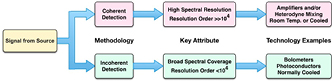
Figure 21. Fundamental detection methodology selection path.
Download figure:
Standard image High-resolution imageFabrication of sensors becomes increasingly challenging at higher frequencies due to the need to minimise parasitic effects that curtail frequency response and limit usable bandwidth. This requires further device miniaturisation and greater consideration of material properties that limit sensor response and sensitivity, e.g. carrier velocity, dielectric effects and resistive losses. For Earth observation, evolution of semiconductor detector technology is required to allow use at supra-THz ( 1 THz) frequencies and relevant developments are described in section 16. For astronomy, similar evolution of superconducting detectors is necessary, including higher ambient temperature operation.
Sensor packaging influences coupling to the incident signal and the pixel count of imaging arrays. It also impacts payload mass and volume and is particularly important with regard to THz heterodyne systems where the provision of local oscillator power is technically demanding and integration with the mixer detector is highly desirable. Mechanical fabrication technologies therefore need advancement to realise minute structures required to both house high-frequency sensors and provide optimum signal matching and some new techniques are considered in section 7. System integration is essential for future payloads, particularly where multiple frequency and or focal plane array operation is required and including future telecommunication applications as discussed in detail in section 17. Complex, diffraction limited quasi-optical trains comprising high tolerance free-space components, e.g. mirrors, frequency selective surfaces, polarisers, and precision calibration mechanisms, must be realised in a compact form that minimises mass and volume. Additionally, signal-processing systems must be enhanced to allow increased digital sampling speed and data processing with reduced power consumption and requires, for example, the development of radiation tolerant complementary metal-oxide semiconductor application specific integrated circuits.
The above present considerable challenges to device and system developers. They will require enhanced electromagnetic and mechanical software modelling methodologies that are complemented by micro-miniature fabrication techniques that enable the realisation of state-of-the-art payload technology.
Concluding remarks.
Deployment of THz technology in space has gained considerable heritage through scientific applications that include astronomy and Earth observation. Excellent potential also exists for increased spaceborne commercial exploitation in support of, for example, weather monitoring and future ultra-high frequency telecommunications. Next generation instrumentation must, however, be compliant with small satellite payload platforms and exhibit low mass, minimal volume, and efficient power consumption. Evolution of sensors to higher frequencies with greater sensitivity and improved imaging capability together with enhanced digital signal processing is also necessary. These technical enhancements present considerable challenges and require developments in, for example, detector materials, circuit miniaturisation, advanced machining, lightweight composites, and improved cooling technologies. Addressing these challenges will allow a wider exploitation of the THz domain from space and important advancements are correspondingly being made within relevant organisations world-wide. Spaceborne THz technology will continue to flourish during coming decades providing both scientific and commercial return.
15. Terahertz components and systems for defence and security imaging
Ken B Cooper1 and Roger Appleby2
1 Jet Propulsion Laboratory, California Institute of Technology, Pasadena, CA, USA
2 Innovasec Ltd, 212b West Malvern Road, Malvern, Worcs, WR14 4BA, UK
Status.
RF systems operating above 150 GHz are poised to find a sustained niche in security applications, with two tipping points recently emerging. First are new standoff body-scanning imaging approaches for checkpoint screening, loss prevention, customs, and intelligence gathering. From distances of many meters, covert crowd-screening is possible that, owing to trade-offs between resolution and aperture size, cannot be accomplished using the longer wavelength millimetre-wave portal systems widely used in aviation security. The Thruvision series of passive imagers from Digital Barriers is the most prominent >150 GHz system commercially available [171]. Another passive imager is that of Asquella, based on cooled microbolometers [172] originally developed at VTT and NIST. Three imagers that operate at either 340 or 680 GHz, which are noteworthy for their relative maturity amongst many active research groups, are JPL's imaging radar (figure 22(a)) [173], the combination radar + passive imager under development by the European concealed object stand-off real-time imaging for security (CONSORTIS) team [174], and the THz-Videocam system from Germany [175] (figure 22(b)). The second development promising wider applicability of THz security technology is the demonstration of InP integrated circuits that open frequency bands up to 850 GHz for use in radar, navigation, and communication. For example, JPL has demonstrated equivalent performance of the system of figure 22(a) with its front-end driven by 340 GHz MMICs developed by Northrop Grumman Aerospace Systems [176] under the DARPA THz Electronics Program. Another near-term application currently receiving intense attention is using the 230 GHz band for imaging through degraded atmospheric environments, such as landing helicopters in brown-outs or targeting from aircraft through low-altitude clouds [177]. In general, THz frequencies are useful in security applications for three reasons:
- 1.Miniaturization of RF hardware: components scale with wavelength, leading to wider deployment opportunities—for example, wearable devices, small aircraft, and small satellites (e.g. see section 14). The ~100 µm length scale of THz devices is also commensurate with lithographic manufacturing techniques (e.g. see section 7), leading to novel THz uses of micro-coax, MEMs devices, artificial dielectrics, and micro-lens antenna arrays.
- 2.High information content: the huge bandwidths available at THz frequencies (tens of GHz) improves spatial resolution of radar and imaging systems, and enables communication with high data rates (also see section 17).
- 3.Unique phenomenology: certain detection capabilities are impossible in any other electromagnetic band, such as molecular fingerprinting via rotational spectroscopy, high-resolution penetration in optically opaque conditions (as described in the section 13), micro-Doppler sensing with simultaneous range resolution, and high sensitivity to scattering from submillimetre scale particles (e.g. micrometeoroids and orbital debris fields that threaten satellites).
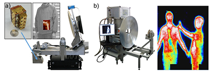
Figure 22. (a) JPL's imaging radar showing a snapshot of an 8.3 Hz frame rate video revealing a handgun inside the pocket of an insulated rain jacket, obtained using a four-element, 340 GHz heterodyne transceiver front end. (b) Hardware and standoff imagery of a checkpoint scenario for the 350 GHz passive imager from the German collaboration of [175] reproduced with permission from Springer, Copyright 2015, where 25 Hz frame rates are achieved with a 128-element detector array. The larger field of view and higher frame rate of the passive system are a consequence of its higher number of detectors.
Download figure:
Standard image High-resolution imageCurrent and future challenges.
The challenges confronting the aforementioned THz body scanners are likely representative of THz security systems more broadly, and here we highlight two primary ones: component cost and signal acquisition. The cost of RF components increases sharply with frequency. For example, a $50 mixer at 5 or 10 GHz might be two orders of magnitude more expensive at 0.5 or 1 THz. (Cost is also addressed in section 16). With other THz-specific subsystems that lack a mass market, such as precision reflector optics and closed-cycle cryogenics (used in some passive imagers), system costs can become prohibitive. Meanwhile, the signal acquisition problem for THz imaging is multidimensional. The achievement of true video rate (30 Hz) imagery requires overcoming difficulties in integrating many THz sensors in a detector array, all calibrated simultaneously, with a low latency back end processor. Imaging over a wide enough field of view (typically dozens of beam widths) is also challenging when reflector antennas are used because of beam aberration off boresight. This can be surmounted with digital beam steering or synthetic aperture approaches, as is done in some W-band imaging systems [178], but the maturity of phased array technology at THz frequencies is currently very low. The importance of the beam-scanning problem has led to a new DARPA program, advanced scanning technology for imaging radars (ASTIR), to overcome current bottlenecks in mechanical subreflector scanning technology. Another major signal challenge, often overlooked in the literature that presents imagery obtained under only favourable laboratory conditions, is the extraction of useful information from clutter such as multi-path confusion for radar systems, and uncontrolled scene illumination for passive imagers. Finally, there is a software challenge of developing THz-imaging-specific automatic threat recognition algorithms to enable more reliable and affordable deployment of checkpoint scanners with minimal operator engagement.
Advances in science and technology to meet challenges.
Many THz technologies that are promising for improving performance or lowering cost of imaging systems, such as compact vacuum electronics, THz lasers, and devices utilizing less mature materials (e.g. carbon electronics) or electromagnetic design principles (e.g. plasmonic devices), will require substantial development times before they prove widely applicable. Similarly, remote sensing solutions for materials identification using standoff THz spectroscopy have not yet demonstrated a path toward general applicability [179]. In the near future, we believe that the trends of past decades suggest that integrated circuits operating above 150 GHz are the most likely devices to enable new THz security systems. For InP transistors that approach 1 THz, advances in scaling gates to 25 nm and below with high yield will require improvements in lithographic processes and metrology reliability during fabrication. Meanwhile, MMICs above 100 GHz using (Bi-)CMOS foundries compatible with mass production promise huge savings in cost and power, enabling applications that use digital beam-forming and ultra-high bandwidth communication. While transceiver circuitry matures, further advances are needed in the digital transistors' scaling and 3D/multi-gate architectures to achieve higher-speed data converters and wider bandwidth digital signal processing. An attraction of passive THz detectors is that high frequency transistors are not needed because densely integrated bolometer arrays, originally developed for astrophysics applications, can be fabricated in a single batch with simple readout circuitry. One example is the kinetic inductance detector (KID) technology, shown in figure 23 [180], which when employed in the CONSORTIS system will have 65 644 pixels at 500 GHz with an NEDT of 0.4 K and 16 416 pixels at 250 GHz with an NEDT of 0.3 K. Also critical for integrated THz electronics are advances in component packaging. For example, dense, high precision waveguide networks made using additive or lithographic fabrication can improve the uniformity and reduce losses in THz source/receiver arrays, and enable efficient power combining of Schottky diode frequency multipliers high power sources above 150 GHz. Examples are Nuvotronics' 230 GHz splitter/combiner network using polystrata waveguide routing [181], and JPL's micromachined silicon waveguide used in the 340 GHz transceiver of figure 22. Accompanying packaging advances, much lower-loss and/or higher-bandwidth passive devices would be immensely helpful for THz systems to mirror the success of lower frequency technology, especially flexible waveguide, substrate antennas, switches, phase shifters, and isolators/circulators.
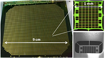
Figure 23. Focal plane array of about 2500 thermal kinetic inductance detectors (left), with optical (upper right) and scanning electron micrograph (lower right) of individual detectors.
Download figure:
Standard image High-resolution imageConcluding remarks.
We have presented the trends and future challenges in THz security systems using the framework of standoff imaging systems. Whereas solid state transistors will likely replace Schottky diodes as sources and receivers in active systems, for passive systems above 150 GHz the large number of receivers (1000s) required to achieve reasonable contrast mean that bolometer arrays continue to be critical, until packaging makes MMICs competitive. For both active and passive systems we therefore predict, with moderate confidence, that integrated circuit and packaging technologies are the highest priority research challenges to achieve lower costs and more widely applicable capabilities. But whatever the route THz technology development takes, we are much more certain that THz systems generally can open sensing modalities simply not possible in any other electromagnetic band.
16. Semiconductor device based THz detection
D Pardo1, P G Huggard1 and V Krozer2
1 Millimeter Wave Technology Group, STFC Rutherford Appleton Laboratory, Didcot OX11 0QX, UK
2 Goethe-Leibniz Terahertz Center, Goethe University of Frankfurt am Main, 60323 Frankfurt am Main, Germany
Status.
We discuss two terminal, majority carrier, semiconductor devices, primarily based on Schottky barriers with GaAs and InGaAs, which underpin a large part of measurement technology at frequencies from below 100 GHz to above 1 THz. Originally configured as point contact devices for frequency multiplication and heterodyne detection [182], this approach has now been supplanted by the more reproducible and reliable airbridged planar technology [183]. Variations of such devices are critical for frequency multiplication to generate local oscillator (LO) signals for heterodyne detectors for radio astronomy [184], for remote sensing of the Earth's atmosphere [185] and for laboratory test and measurement instruments [186]. The same approach is also used for the transmit elements in radars and communication systems. As heterodyne mixer detectors, Schottky diodes dominate in nearly all the above fields, the exception being radio astronomy. They offer a low conversion loss, typically better than 10 dB, room temperature operation and intermediate frequency (IF) bandwidths extending to tens of GHz. Applications are indicated in sections 14, 15 and 17. This section also complements the discussions in sections 5 and 6.
Device topologies range from single anode devices used in direct detectors, through anti-parallel pairs in sub-harmonic mixers (figure 24) to the multiple anode series and anti-series configurations needed for multipliers handling high input powers. Traditionally, devices are diced and soldered to gold on quartz microstrip filters, which are then embedded in single mode waveguide cavities. This approach has evolved to using self-supporting membranes for THz frequencies and high thermal conductivity substrates for high power multipliers. The combination of microstrip and waveguide cavity achieves the required impedance matching over wide instantaneous bandwidths, at RF, LO and IF for mixers. As these are square-law devices, Schottky diodes also function well as video detectors, and either waveguide or quasi-optical mounts can be used for fast, broadband room temperature detectors with a wide dynamic range [187].
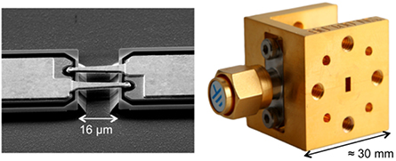
Figure 24. Photographs, left, of an anti-parallel pair of airbridged Schottky diodes and, right, of the typical waveguide block in which the diode circuit is embedded. Photos courtesy of MMT group, RAL space.
Download figure:
Standard image High-resolution imageFurther advances will bring easier design and manufacture, greater output power through improved power handling and efficiency, wider operating bandwidths and improved THz performance and integration with devices offering, for example, low noise RF and IF amplification, power RF amplification and photonic LO provision.
Current and future challenges.
The main challenge is how to maintain device performance as frequency increases. Figure 25 above shows the increase of Schottky mixer conversion loss with frequency, from typically 5 dB at 100 GHz to 10 dB at 1 THz, and the corresponding rise in noise temperature, following approximately 50 times the quantum limit, hν/kB. Similar plots for frequency doublers show a roll off of power conversion efficiency from tens of percent below 100 GHz to a few percent above 1 THz. The corresponding tripler figures are a few percent at 100 GHz and below 1 percent above 1 THz.
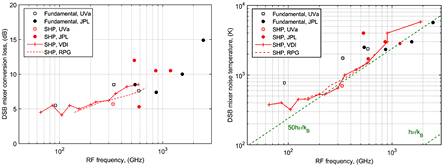
Figure 25. Performance of Schottky mixers as a function of frequency. Left hand graph shows double sideband conversion loss and, right, corresponding mixer noise temperature. Adapted with permission from [188].
Download figure:
Standard image High-resolution imageTo improve individual detector performance, the challenge is to design simultaneously at several frequencies, including the passive waveguide and microstrip with the electrically nonlinear Schottky device, and the antenna structure in the case of a quasi-optical mount. Mutiple frequency design is needed to optimise impedance matching and, for multipliers, to minimise power generation at unwanted frequencies. Imaging and future Earth observation instrumentation requires arrays of detectors, so efficient methods of distributing the LO signal to each pixel are needed: this will also benefit radio-astronomy. Generating a frequency multiplied LO with increased efficiency and lower component count is also required: the current cascading of several x2 and/or 3x multiplication stages to reach THz frequencies is cumbersome and inefficient, with the packaging overwhelmingly dominating the device volume: figure 24. Improved multiplier design tools are also needed: the challenges are as for mixers, with the added complexity of thermal dissipation and the thermal nonlinearity in the Schottky device(s). As performance decreases at elevated temperatures, methods of overcoming the relatively poor thermal conductivity of GaAs are needed. Device area also drops with increasing frequency, to minimise parasitic shunt capacitance, so methods of applying several devices in parallel and combining their outputs to achieve higher power are required.
The challenge of integration of Schottky devices with photodiodes or high frequency transistors also needs addressing, for example to produce mixers with photonic local oscillator generation and integrated IF amplifiers respectively. Composite circuits are currently assembled from discrete devices produced in different laboratories, from dedicated wafers grown and processed by optimised methods in each case. Very little effort has been invested in growing and processing to demonstrate more than one technology on the same chip.
Advances in science and technology to meet challenges.
Improved design tools, changes in device topology and new materials will be needed so that the performance of Schottky technology improves at frequencies close to and above 1 THz and that the cost of anticipated volume applications, for example in short range communications, at frequencies up to a few hundred GHz, drops.
Improved design techniques will require the application of Monte Carlo and hydrodynamic models, in parallel with the conventionally used HFSS/CST and ADS modelling combination. Accurate knowledge of the complex dielectric properties of metals, dielectrics and doped semiconductors at THz frequencies will be needed as inputs to the models. It is also assumed that the application of thermal modelling will be routine. Instead of modelling individual Schottky devices driving a set of impedance matched ports, as done now, the interaction with immediately adjacent devices will be included. Collectively, this means that much more computing power will be needed for the design process.
As mentioned above, the current approach of connecting devices by single mode waveguide is inefficient, but it does offer the advantage that the inevitable loss in the microstrip to waveguide to microstrip transitions offers some isolation and reduces the standing waves that modulate the devices' performance with frequency. A new approach to connecting a series of Schottky devices in a single block, with intermediate microstrip components offering isolation via circulation or attenuation should be used.
New materials and processing approaches will be needed: at low frequencies GaN has potential and more generally composite semiconductors will provide the necessary high thermal conductivity path that is needed from the Schottky anode. For comparison, the thermal conductivities of Si and AlN are roughly three times that of GaAs, and that of CVD diamond is an order of magnitude higher again. For integration, dedicated wafer growth will include the required layers to permit definition of optical waveguides, photodiodes and transistors adjacent to the Schottky device, and process development will permit contact deposition and annealing without adverse effects on other devices.
Concluding remarks.
Schottky devices, made from GaAs and its alloys, will continue to be the most widely applied terahertz detector technology, due to their critical role in test equipment and scientific instrumentation. This includes mixers, with associated frequency multipliers for LO provision, and power detectors. For specific video detection applications, CMOS transistor detectors may be employed [189], but the high initial cost of a wafer run is a barrier to widespread application. High CMOS device impedance restricts the IF bandwidth, making the technology unattractive for mixer applications. However, both direct and mixing functions have been demonstrated in GaAs alloy based heterostructure field effect transistors [190]. Space limitations prevents discussion of other detector devices, e.g. ternary tunnel diodes [191].
Investment in the parallel application of numerical simulations by high power computers, composite semiconductor growth and ambitious integration projects will deliver a step change in the way GaAs devices perform, will physically shrink interconnects and packaging, and achieve the needed integration with other semiconductor technologies.
The authors thank Byron Alderman for his comments.
17. Status of THz communications
Haymen Shams1, Martyn Fice1, Cyril Renaud1, Alwyn Seeds1 and Andreas Stöhr2
1 Department of Electronic and Electrical Engineering, University College London, Torrington Place, London, WC1E 7JE, UK
2 Department of Optoelectronics, Faculty of Engineering, University of Duisburg-Essen, Lotharstr. 55, 47057 Duisburg, Germany
Status.
Wireless data traffic is increasing exponentially, as mobile users increasingly make use of online services. It is expected that global mobile data will grow up to 24.3 Exabytes monthly by 2019 [192]. This huge increase results from the deployment of broadband networks for fixed and wireless communications, and the evolution of new online services such as video streaming, and cloud-based applications. Therefore, there is need for new wireless technology that supports much higher wireless speeds. Although Wi-Fi is the most popular form of wireless communication, its capacity is still limited with worldwide assigned bandwidth. Wider spectral bands are available at millimetre-wave (mm-wave) frequencies, such as 60 GHz, and 70–95 GHz, while the total allocated bandwidth is less than 7 GHz, which support data rates of 10 Gbps over short distances. For higher capacity wireless data systems, THz communication bands (0.1–10 THz) are being investigated for their much larger available bandwidth, which ranges from a few GHz to over 1 THz. Although optical frequencies can offer even larger bandwidth, the optical beams have very small tolerances in line-of-sight alignments, and two orders of magnitude higher losses due to weather conditions such as fog (200 dB km−1) and scintillation effect, compared to little or no effect for THz waves up to 1 THz [193, 194]. This makes photonics-enabled THz wireless a more attractive systems solution.
Several research groups have demonstrated communication links in the W-band (75–95 GHz) and for frequencies over 100 GHz. Real time transmission was reported based on on–off keyed (OOK) modulation using a Schottky barrier diode for direct detection scheme, and polarization multiplexing in a multiple input multiple output (MIMO) system for 48 Gbit s−1 dual channel at 300 GHz [195]. Other THz wireless link demonstrations have been carried out based on offline detection, where the wireless signal is down-converted to intermediate frequency (IF) and digitally processed offline. This scheme improves the receiver sensitivity and the system quality by correcting the transmission impairments using advanced digital signal processing (DSP). Multiple wireless channels at sub-THz frequencies were proposed to use the available spectrum and reduce the bandwidth limitation of the optoelectronic components [196, 197]. Recently, a multiband sub-THz system was demonstrated for downlink transmission with an overall downlink channel data rate of 100 Gbits s−1 and uplink rate of 10 Gbit s−1 OOK (figure 26) [198]. Also, researchers from Université de Lille demonstrated a THz wireless communication system operating at a higher carrier frequency of 400 GHz with up to 46 Gbit s−1 OOK by using a THz photo-mixer integrated with a broadband antenna [199].

Figure 26. Photonic multiband wireless over fibre system. (OFCG: optical frequency comb generator, PD: photodiode, E/O mod: electro-optic modulator, OF: optical filter, UL Rx: uplink receiver, DSP: digital signal processing).
Download figure:
Standard image High-resolution imageCurrent and future challenges.
The fundamental challenges at these THz band frequencies are high path loss, and atmospheric absorption due to water vapour molecules. Beside these the low source power and large down-conversion loss require the use of directional and line-of-sight systems instead of the omni-directional antennas used at lower frequencies. Synergies between fibre and THz wireless links enable THz signal distribution over wide areas, while maintaining the same power budgets. In addition, all the resources of optical communications and photonic methods can be adapted to provide high spectral efficiency data modulation formats, wavelength division multiplexing technology for multichannel THz wireless links, and coherent optical receivers for impairment compensation. These considerations make photonic generation of high-bandwidth mm-wave signals attractive, although impressive work was reported on fully electronic systems at frequencies above 200 GHz [200].
Photonic integration technology can play an important role to provide an efficient and reliable solution for THz wireless over fibre (WoF) in terms of cost and size. However, there is still need to develop integrated THz sources with lower phase noise. Another key challenge for THz WoF is the realization of high optical responsivity, large bandwidth and high power photodiodes (PDs) such as the uni-travelling-carrier (UTC) PD. The use of UTC-PD arrays can be explored to increase output power. Such arrays also enable advanced active beam-forming antennas, which can compensate for path loss and enable mobile device tracking. The challenge of supporting the large bandwidth for multi-Gbit/s links without beam squint will be significant. However, it will be an opportunity for beam steering capability and MIMO systems. Even if photonic THz signal generation is employed at the transmitter, low-loss and wide-bandwidth down-converting mixers are required at the receiver as discussed in section 16. In-phase/quadrature mixers down-converting direct to the baseband are not yet available at mm-wave frequencies, but should give improved performance, and would allow exploitation of DSP hardware and algorithms developed for optical fibre communication systems.
Uplink data transmission is another issue for realizing duplex transmission links. Mobile device power constraints may make it attractive to use lower frequencies and reduced data rates for uplinks depending on service requirements.
Advances in science and technology to meet challenges.
Optical fibre offers many advantages as a transmission medium for high capacity data transmission. Because of these advantages a photonic approach for high frequency signal synthesis and distribution is beneficial over more conventional techniques, using electronic oscillators with multipliers. The most promising photonic technique for optical signal generation is the heterodyning of two optical sources with different wavelengths using a photodiode or other photomixing device. The heterodyned signal is an RF signal at the difference frequency between the two optical sources. This exhibits phase noise fluctuations resulting from the instability of both lasers. Photonic integration of a monolithic dual-wavelength source for mm- and THz-wave generation is attractive as it results in more compact, tuneable sources and can give improved spectral purity.
One approach is based on the monolithic integration of two distributed feedback lasers grown side by side and combined using a coupler as shown in figure 27(a). This approach is compact and both lasers encounter the same environmental fluctuations, thus reducing noise in the heterodyne signal. However, the spectral purity of the generated THz signal is determined by the summed linewidth of the lasers and their frequency instability due to laser thermal drift or mode changes. Several techniques were developed to achieve high spectral purity THz signals based on optical comb sources, where a number of phase correlated optical tones can be generated using either fibre or semiconductor based devices. The comb lines required for heterodyning can be selected using conventional optical filters, but more effective filtering can be achieved by using other photonic techniques such as optical phase lock loop (figures 27(b) and (c)). Due to stringent loop delay requirements, such approaches will rely on photonic integration coupled with carefully designed electronic feedback circuits. A key development here is the move to foundry-based photonic integration enabling reduced development time and closely defined performance, with resultant cost savings.
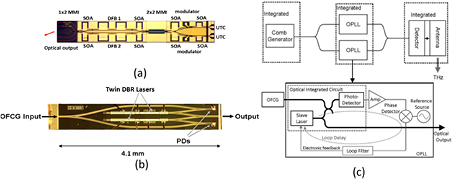
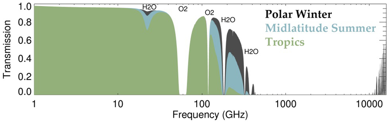
Figure 27. Microscope view of monolithic photonic integration of (a) dual DFB dual wavelength source [201] and (b) a dual OPLL [202], and (c) schematic diagram of tuneable coherent THz source. (SOA: semiconductor amplifier, DFB: distributed feedback laser, DBR: distributed Bragg reflector, OFCG: optical frequency comb, OPLL: optical phase lock loop). © 2011 IEEE. (a) © 2014 IEEE. Reprinted, with permission, from [201]. (b) and (c) reprinted with permission, from [202].
Download figure:
Standard image High-resolution image
Another key component for THz photonic systems is the photomixer, which should offer simultaneously high saturation power, high responsivity, and high bandwidth. Most recent work points towards the use of photodetectors as photomixers, and, in particular, the use of UTC-PDs as they meet most of the key parameters. Further, photonic integration of those InP-based THz photomixers with Si-based low optical transmission loss waveguides is needed for developing electronically steerable antenna arrays which are crucial to achieve the SNR required for spectral efficient THz communications [203]. Advances in mm-wave electronic subsystems will also be required for practical and cost-effective THz communication systems, especially power amplifiers and phased-array antennas.
Concluding remarks.
The need for bandwidth to support high capacity wireless data transmission is a strong driver for the development of THz communication systems. There are a number of transmission windows in the spectrum below 400 GHz that are well suited to short range and indoor wireless systems.
The most important challenges for commercial realisation of this technology are the development of compact and efficient THz sources providing continuous wave output power levels up to 100 mW and the development of compact electronically steerable antenna arrays to minimise wireless link loss.
18. Metrology for THz technologies
Mira Naftaly1, Nick Ridler1 and Roland Clarke2
1 Division of Time, Quantum and Electromagnetics, National Physical Laboratory, Teddington, TW11 0LW, UK
2 School of Electronic and Electrical Engineering, University of Leeds, Leeds, LS2 9JT, UK
Status.
The area of terahertz science and applications has been growing roughly exponentially since the invention of time-domain spectroscopy in the early 1990s (see section 8), as indicated by the number of scientific publications. However, it is only in the last few years that the field has matured to the degree that metrology and standardisation have gained focused attention, resulting in an increasing number of publications and a book devoted to the subject [204].
Measurements at THz frequencies employ two disparate classes of instrumentation platforms: free-space and waveguide-based. Whereas free-space techniques have evolved from optical spectroscopy by expanding the operational range to longer wavelengths, waveguide-based approaches are an extension of electronic RF measurements to higher frequencies. In a sense, the increasing bandwidth overlap between these technologies represents the continuing shrinkage of the so-called 'THz gap'.
Free-space and waveguide techniques occupy different and separate spheres of THz applications, in that free-space measurements are employed primarily for material spectroscopy and imaging, whereas waveguide measurements are utilised for device characterization. Although state-of-the-art waveguide-based devices overlap the lower frequency range of free-space instruments, nevertheless the two types of THz measurements remain distinct, divided by both areas of application and experimental methodologies. Their metrological problems and challenges are also different, and for that reason will be discussed separately.
Free-space THz spectroscopy is mainly accomplished by two types of instruments: Fourier transform spectrometers (FTS) and time-domain spectrometers (TDS). Although both rely on the Fourier transform to derive spectral data, they are in other respects significantly different, operationally and metrologically. The most important distinction is that TDS is a coherent technique, that is to say, it measures directly the time-varying electric field of the THz pulse, yielding both field amplitude and phase; whereas FTS is incoherent, measuring only field intensity. As a direct consequence, TDS provides a straightforward means of determining unambiguously the refractive indices and absorption coefficients of materials studied. In contrast, parameter extraction from FTS data is complicated, requiring specially prepared samples and measurements in both transmission and reflection geometries, and results in large uncertainties. Moreover, TDS systems can achieve (and typically demonstrate) much larger signal-to-noise ratio and dynamic range than FTS instruments. For that reason, TDS dominates measurements of optical constants of materials. FTS, on the other hand, is preferentially employed in measurements requiring ultra-wide bandwidth from sub-THz to mid-IR. Complementary to TDS and FTS, non-spectroscopic or narrow-band THz measurements, including imaging, have been performed using a variety of emitter-detector combinations, and are often employed in types of applications where metrological considerations are of secondary importance (see sections 6 and 13).
Waveguide-based THz measurements are predominantly made using heterodyne vector network analyzer (VNA) based systems [205], whose operational bandwidth and upper frequency limit has been steadily increasing and now extends to THz frequencies. This has been achieved using frequency extender heads that are external to the VNA and that operate using harmonics of the fundamental of a microwave signal source. VNA systems employ coherent detection and enable calibration procedures (i.e. error correction routines) to be applied automatically so that imperfect system hardware is corrected 'in software' without needing to make manual adjustments to the measuring instrument.
Current and future challenges.
The most straightforward of metrology issues in free-space THz measurements is the lack of calibrated traceable power measurement devices suitable for sources which are frequently broadband and typically less than 100 µW. The technological challenge centres on designing a detector with a frequency-independent responsivity over a very large bandwidth and capable of detecting incident power down to a few µW (see section 16). This is being addressed by the team at PTB (Physikalisch-Technische Bundesanstalt, Germany) [206] who have been developing and have now demonstrated a pyroelectric power meter calibrated using radiometric techniques.
FTS is a mature and established technology in the near- and mid-infrared, and its extension into the THz band is relatively straightforward. However, historically it has been used primarily to identify resonance absorption features in a variety of materials. In contrast, THz spectroscopy most often requires accurate determination of the absorption coefficient and refractive index from featureless spectral data, especially in the frequency band where TDS is also available. FTS, however, is less well suited to such measurements, because derivation of these optical constants from intensity data is problematic. Design, performance and parameter extraction using far-IR FTS are thoroughly reviewed in numerous books on the subject, e.g. [207, 208].
TDS, as the newest and least mature spectroscopic technique encounters metrological challenges specific to this modality. Similarly to other instrumental platforms, these are of three types: device configuration and performance; sample effects; and parameter extraction algorithms. One of the most important papers in THz metrology was the analysis of the limits placed on the spectral bandwidth of a TDS by its dynamic range in frequency domain [209]. Similarly, the dynamic range of a TDS in time domain was shown to limit its frequency resolution [210]. Since the dynamic range is in turn limited by system noise, sources of noise are an important parameter of TDS performance. The greatest attention has been accorded to the methods of parameter extraction, where calculation procedures have been proposed and analysed by several authors, e.g. [211, 212]. The uncertainties in the obtained optical constants (absorption coefficient and refractive index) have also been analysed in detail, e.g. [213, 214].
Free-space THz measurements are currently encountering several different metrological problems, which also vary among the instrumentation platforms. FTS and TDS share a significant problem in the lack of agreed calibration standards or artefacts for the THz band. Because measurements at THz frequencies are used to determine the optical constants of materials, standards are required for frequency, optical thickness (phase delay) and loss. There is also a lack of rigorous measurement intercomparison studies between FTS and TDS. In addition, several metrological issues specific to TDS have not yet been adequately addressed. The most important of these are: the effects of instrument performance and of different THz beam path configurations; and the accuracy of different methods of parameter extraction and their suitability to various types of sample. An international intercomparison study of different TDS systems and measurement techniques is currently taking place, aimed at resolving some of these questions.
Current VNAs enable measurements to be made at all frequencies up to 1.1 THz. This is achieved by using harmonic multiplying and mixing which takes place in extender heads that are attached to the VNA. A pair of extender heads, fitted with waveguide test ports, is needed so that two-port devices (i.e. devices with both an input and an output) can be measured using signals propagating in both forward and reverse directions.
The aperture size of the waveguide is chosen to support the required frequency range; standardised waveguide sizes are available for frequencies to 3.3 THz and beyond [215]. Measurements can also be made on planar wafer substrates by attaching probes to the waveguide test ports; these are currently available at frequencies up to 1.1 THz [216]. Obtaining the required machining tolerances of waveguides used at THz frequencies is a major technological challenge. These tolerances give rise to both random and systematic errors in measurements made using waveguides, which arise from interface reflections when two connected waveguides are either misaligned or have slightly differing aperture dimensions (height and width) [215]. Although reflection losses in pristine, optically polished metals are well known, variations in waveguide losses arising from surface defects, oxidation and roughness have not been investigated or quantified.
Advances in science and technology to meet challenges.
The metrological challenges in free-space THz measurements are primarily organisational rather than technological. International standards must be agreed; calibration artefacts must be developed and tested; and procedures for instrumentation and device specifications must be defined.
The most important technological challenge of using metallic waveguides at THz frequencies is to increase the dimensional precision of mechanically machined waveguide components—particularly, waveguide interfaces and apertures, as shown in table 3. Although aperture tolerances of 5.1 µm and 1.7 µm (for a reflection coefficient of −42 dB at mm-wave frequencies) are achievable using current technology, tolerances of 0.50 µm and 0.17 µm (for a reflection coefficient of −42 dB at THz frequencies) are considered beyond state-of-the-art, at least for routine industrial manufacturing capabilities.
Table 3. Required aperture tolerances for −42 dB reflection coefficient to 3.3 THz, and reflection coefficient values achieved by the existing IEEE 1785.2a interface [217] to 3.3 THz.
| Frequency range | Waveguide size | Aperture dimensional tolerances for −42 dB reflection coefficient (µm) | Reflection coefficient due to waveguide interface dimensional tolerances (dB) |
|---|---|---|---|
| 75 GHz–110 GHz | WR-10 | 5.1 | –60 |
| 220 GHz–330 GHz | WR-03 | 1.7 | –39 |
| 0.75 THz–1.1 THz | WM-250 | 0.50 | –19 |
| 2.2 THz–3.3 THz | WM-86 | 0.17 | –3 |
Table 3 also lists the performance of an existing waveguide interface intended for mm-wave and THz frequencies [217], showing that reflection coefficients approaching −40 dB are achievable at frequencies up to 330 GHz, but performance is much degraded at higher frequencies (i.e. 1.1 THz and 3.3 THz). This indicates that improved or new waveguide interface designs are needed for waveguide metrology at THz frequencies.
All the above problems could be resolved by adopting new forms of waveguide (e.g. [87]), provided these can win end-user acceptance.
Concluding remarks.
The broad area of THz measurements is set to continue its rapid expansion, encompassing all types of instrumentation platforms, free-space and waveguide-based. These will require robust metrological underpinning in order to support both scientific research and industrial applications. Several issues demand to be addressed in particular. For TDS these are: establishment of standardised measurement, calibration, and data analysis procedures. For VNA, engineering solutions are needed for high-precision waveguides and interconnects. In addition to these, inter-operability and inter-comparability must be achieved between TDS and VNA measurements.
The ultimate goal is to establish a robust framework of metrological traceability to the international system of units (SI) for the portfolio of measurands (i.e. for physical quantities that need to be measured) that are, and will be, needed to underpin scientific and technological developments in the years to come. This framework will ensure the reliability and equivalence of all measurements made at terahertz frequencies. This is a pre-requisite for effective science, trade and industry that exploits the terahertz region of the electromagnetic spectrum.