

Abstract
A first principles analysis of the behaviour of point defects, namely, self-interstitial atoms, a single vacancy and light impurity atoms such as H and He in tungsten is reported. These defects can be produced in the first wall of the future nuclear fusion reactors due to the high radiation fluxes present. The evolution of defects that appear in the bulk and end up reaching the surface has been followed. An energetic study has been combined with a detailed charge density analysis of the system by means of the SIESTA code. The resulting data have been validated by confronting them with those obtained with a more precise plane wave code, namely VASP. Meanwhile, the structural and the mechanical properties of the system have been positively compared with experimental measurements. Such comparisons have led us to present a new SIESTA basis for tungsten. This complete analysis establishes a nanoscopic view of the phenomena involving the presence of light atoms at native defects in tungsten, paying special attention to the vicinity of surfaces.
Export citation and abstract BibTeX RIS
1. Introduction
In the design of both inertial and magnetic confinement fusion reactors, one of the elements that must support the largest damage due to radiation exposure is the first wall material. As a result of the fusion reaction a large number of isotopes of hydrogen and helium reach the first wall. In principle, the retention of H and He can lead to bubble formation that in turn produces damage in the form of 'swelling', 'embrittlement' and 'creep' [1]. These non-desirable effects dramatically change the properties and operational performance of the material. A well analyzed foreseen candidate for the design of these reactors is metallic tungsten due to its resistance to high temperatures, low sputtering yield, its favourable thermal properties, as a high thermal conductivity, and its interesting macroscopic mechanical properties [2]. These outstanding characteristics can be further improved when tungsten is nanostructured leading to a high density of grain boundaries [3]. This promising material presents a clear advantage with respect to its counterpart with grain size in the micrometer range, the so-called coarse grained tungsten. In particular, the light impurity species like H and He may have a greater mobility along the grain boundaries of the nanostructures [4]. This effect implies that the increase in size of the bubbles, due to the accumulation of the light species, will be delayed with time of exposure. For that reason, in order to understand the behaviour of impurities in nanostructured tungsten it is interesting to study their behaviour in the bulk, on the surface, and at the interface.
The study of the H absorption/desorption in metals is important in chemistry [5] due to their catalytic properties. Several studies have been reported about the configuration of superficial defects and the deformation of the surrounding atoms in the metallic surfaces. To begin with, energy changes have been analyzed for oxygen atoms adsorbed near superficial vacancies on silver [6]. Then, the mobility of vacancy clusters on a copper surface has been studied by Akbarzadeh and co-workers [7]. Finally, the interaction and stability of hydrogen atoms adsorbed on the tungsten surface at different orientations, namely, (1 0 0), (1 1 0) or (1 1 2) has been analyzed by many authors [8–11]. Nojima et al [9] studied the deformation of the layers near the surface obtaining a more stable configuration for a H atom adsorbed on a hollow position at the surface, in agreement with other authors [8, 10]. The energy of the H atoms was calculated depending on the fractional surface coverage (θ) of H, defined as the number of absorption sites occupied relative to the number of absorption sites available. For θ = 1, the energy obtained was 2.12 eV, while for θ = 0.5 the value was 2.4 eV. Johnson et al [8] studied the entire path that leads hydrogen from the surface to the volume. The energy absorption was estimated in −0.75 eV, or −0.71 eV when the zero point energy (ZPE) is included [8]. This value was related to the results of experiments of thermal desorption spectroscopy (TDS) [12] that found desorption peaks located at 1.17 eV/H2 and 1.42 eV/H2. According to Johnson et al [8], the second peak shows a direct relation with the adsorption energy (Eads), as it doubles the calculated energy. However, as discussed more comprehensively in [13], the relationship between density functional theory (DFT) calculations and TDS experiments is not so straightforward. Similarly, previous works studied the interaction of H and He inside the bulk, obtaining the tetrahedral interstitial site (TIS) as their most stable position in W. The corresponding formation energies were 0.89 eV for H [14] and 6.16 eV for He [15].
In this work, we present a complete energetic analysis of the different defects in W bulk proposing a new W basis to be used within the DFT SIESTA code [16]. In order to validate this basis, some energetic results are compared with the well-tested plane-wave code VASP [17]. The structural and mechanical properties have been compared with experimental measurements [18]. Our calculations allow us to relate the results at the surface with those in the bulk. We have analyzed the energies, charge densities and structural configurations of different defects (vacancy and interstitial W, H and He atoms) present at the layers close to the surface. The article is divided as follows: the second section is devoted to the explanation of the methodology. The third section shows the different tests performed to validate our W basis for SIESTA, taking especial attention to the comparison of the mechanical properties with previous experimental data and to the formation energies of the isolated defects calculated in tungsten bulk as well as the combination of a He/H atom inside a W vacancy. In the fourth section, we repeated the calculations of such defects but in positions close to the surface, including a detailed study of the charge distribution for all the cases mentioned before. Finally, we summarize our results in the conclusions section.
2. Methodology
DFT simulations have been performed with the SIESTA (Spanish Initiative for Electronic Simulations with Thousands of Atoms) code [16] that uses a basis of atomic-like orbitals. We have created a new Double zeta (DZ) basis for tungsten with the following cutoff radii (in atomic units): n = 6, l = 0: r(ζ 1) = 5.400 and r(ζ 2) = 3.500; n = 5 and l = 2: r(ζ 1) = 5.000 and r(ζ 2) = 3.000; finally for n = 6 and l = 1, we propose a simple basis inspired by the one presented by Walkingshaw et al in [19] with r(ζ 1) = 5.500. The standard SIESTA double zeta plus polarization (DZP) basis for hydrogen and helium has been used [20]. In order to validate the results, we have performed calculations based on the plane-wave Vienna ab initio simulation package (VASP) code [17]. In SIESTA simulations, we employed the Troullier-Martins pseudo-potentials [21], together with the revised Perdew–Burke–Ernzerhof for solids (PBEsol) parametrization of the generalized gradient approximation (GGA) for the exchange and correlation functional [22]. On the other hand, for the VASP simulations, we used the original Perdew–Burke–Ernzerhof (PBE) approximation [23] for the exchange and correlation functional and the projector augmented-wave (PAW) pseudo-potentials provided by VASP [24]. The energy cutoff for the plane waves was 479 eV, i.e. the default value for He as given by the VASP code. The first Brillouin zone is sampled by 8 k-points within a 2 × 2 × 2 Monkhorst-Pack scheme [25] for the bulk calculations and by 4 k-points within a 2 × 2 × 1 scheme for the surface. In both simulations with VASP and SIESTA codes a Methfessel–Paxton smearing was used with a broadening of 0.2 eV [26].
The defects will be incorporated to a big enough supercell representing the bulk. In our calculations, a 4 × 4 × 4 cubic unit cell (128 atoms) is generated, in the bcc structure for α − W phase (see section 3.1). Then, the formation energy is estimated with the general standard expression for the different defects included:

where Etot(nV + NHe/H) is the energy obtained after the relaxation of a system with n vacancies and NHe/H He or H atoms, respectively, Ebulk(NW) is the energy of one W atom in the perfect W bulk supercell of NW atoms and finally, Eat(He/H) is the energy of one isolated He atom or half the energy of a H2 molecule [½ Emol(H2)] in the same 4 × 4 × 4 cubic unit cell.
On the other hand, the surface calculations have been performed for 10 atomic layers following the W(1 1 0) orientation (corresponding to the most stable surface found in nanostructured tungsten, see section 3.1) with a 6 × 3 periodicity and fixing the last two layers in the bottom part of the slab (36 atoms) to mimic bulk behaviour. For this system, the formation energy at the surface, compatible with equation (1), is defined as:

where now Esurf(NW) is the relaxed clean surface energy and NI is the number of the so-called self-interstitial atoms (SIAs), i.e. W atoms out of their original bulk positions. The different bulk and surface configurations have been relaxed until the interatomic forces are lower than 0.05 eV Å−1. The SIESTA code, having localized orbitals with finite radius, must be corrected by the Boys and Benardi method [27]. The system is corrected by introducing the so-called ghost atoms where the basis is represented without nuclei or charges. For the calculation we use the following expression:

where EA/B is the energy of the isolated systems A or B and EAB* is the energy for system A replacing B with ghost atoms and vice versa. See [27] for more details.
Charge analysis is performed using the method of Mulliken Population Analysis [28], as implemented in the SIESTA code. Using the atomic-like orbital basis, the charge around each atom is determined within this methodology. The use of the atomic and orbital charges allows the estimation of the electronic interaction between tungsten atoms and the different defects.
3. W basis tests
In order to validate the W basis mentioned above, three different tests were carried out.
3.1. Assessment via experiments: mechanical and structural properties
The first test was to compare the simulated and experimental results. The structural and mechanical properties characterizations were carried out in two kinds of samples: nanostructured W (NW) and commercial coarse grained W (CGW). The fabrication of NW is described as follows: the nanostructured W coatings were deposited by DC magnetron sputtering from a pure W commercial target (99.95%) in the presence of a pure Ar atmosphere (99.9999%) at constant Ar pressure (P = 8 × 10⁻³ mbar). The plasma power was set at 39 W (260 V and 150 mA). These NW coatings consist of compact nanocolumns with an average diameter of 150 nm and about 2 μm in thickness. Structural characterization of the samples was carried out by x-ray diffraction (XRD) using a Philips X-PERT four cycle diffractometer with a CuKα (λ = 0.15 405 nm) radiation source. XRD measurements were performed in Bragg–Brentano geometry. The θ − 2θ XRD pattern is shown in figure 1. The results indicate that both NW and CGW are polycrystalline made of pure bcc α − W phase with a preferential (1 1 0) orientation. The lattice parameter was calculated from the position of the centroid (1 1 0) by Gaussian fitting and the Bragg's law to be 3.163 Å for the NW coating and 3.165 Å for the CGW sample. The mechanical response of the coatings was evaluated by nanoindentation tests. The indents were performed by using a MTS Nanoindenter XP and the continuous stiffness measurement technique together with a diamond Berkovich indenter. The calculated Young's modulus was 390 GPa for the NW coating and 402 GPa for the CGW. More information about the NW coatings deposition processes and characterization can be found in references [3, 18].
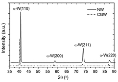
Figure 1. XRD pattern of NW coating (black line) and CGW sample (dashed line). The Bragg peaks corresponding to the α − (1 1 0), α − (2 0 0), α − (2 1 1) and α − (2 2 0) reflections of the thermodynamically stable bcc α − W phase are indicated.
Download figure:
Standard image High-resolution imageThe lattice parameter from the simulations was estimated to be 3.167 Å, being in good agreement with our experimental results and other data found in the literature, 3.165 Å [29]. The second parameter to be compared with the experiment is the Young's modulus. This parameter was calculated, by adding a 1% strain along each direction of the bcc structure to obtain the different components of the elastic tensor, Cij. For the highly symmetric metals, the expression for the Young's modulus is: E = (C11 * C12 + 2) * (C11 − C12)/(C11 + C12). The calculated value is 410.6 GPa, also in good agreement with the experimental result quoted previously. Finally, the bulk modulus obtained was 315 GPa again in good agreement with the experimental value of 310 GPa presented in [29].
The agreement between the simulations and experimental data indicates that the W basis proposed for the SIESTA code has positively passed the mechanical and structural properties test.
3.2. Single defects in Tungsten Bulk
The second test consists in a comparison of the formation energies of the main point defects to the results obtained with the well-tested VASP code. Table 1 shows the defect formation energies estimated by SIESTA versus VASP. The first case will be the SIAs. Our attention will be focused on the most stable cases shown in figures 2(a) and (b): the dumbbells along directions 〈1 1 0〉 and 〈1 1 1〉 (denoted as d110 and d111, respectively). The results from SIESTA seem to be overestimated, i.e. the formation energy for d111 is 10.35 eV versus 10.08 eV from the VASP calculations. Nevertheless, it is worthwhile to mention that the difference in the formation energies between defects d110 and d111 remains quite stable, being 0.12 eV and 0.20 eV, with SIESTA and VASP, respectively. These differences are close to the values reported by Becquart et al [15] (0.26 eV) and Nguyen–Manh et al [30] (0.30 eV).
Table 1. Formation energies values of the different defects: SIESTA versus VASP.
| SIAs | SIESTA (eV) | VASP (eV) | Impurities (eV) | SIESTA (eV) | VASP (eV) |
|---|---|---|---|---|---|
| d111 | 10.35 | 10.08 | H_oct | 1.19 | 1.35 |
| d110 | 10.47 | 10.28 | H_tet | 0.80 | 0.96 |
| d100 | 12.30 | 12.09 | He_oct | 6.66 | 6.49 |
| Oct | 12.21 | 12.21 | He_tet | 6.45 | 6.25 |
| Tet | 11.47 | 11.49 | W-Vac | 3.11 | 3.16 |
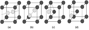
Figure 2. Ball and stick models showing the most interesting defects studied: (a) d110 ; (b) d111; (c) H/He in an octahedral position; (d) H/He in a tetrahedral position.
Download figure:
Standard image High-resolution imageOther kinds of interesting defects are the light impurity atoms like hydrogen or helium. They can be accommodated in the two highly symmetric positions in the bulk: the octahedral interstitial site (OIS) and the previously defined TIS as shown in figures 2(c) and (d), respectively. For both impurities (H and He) the TIS is the preferential site. Again, the formation energies of the impurities differ between 0.15–0.20 eV respect to the values obtained with the VASP code (see table 1 where all these values are summarized), suggesting that the lower deformation induced by the light H or He atoms in the system has a relatively small effect on the formation energy. The differences between the formation energies of TIS and OIS sites are 0.21 eV for He and 0.39 eV for H in good agreement with the VASP results.
In figure 3, the valence charge density of one He and one H atom is shown for both TIS and OIS sites inside the W crystal. While in the He case the interaction with the W atoms is very low, the H atom case presents a remarkable electronic interaction with four/two surrounding neighbours in the TIS/OIS site, respectively. This is observed in the projections of figure 3 where the H atom (in blue) in the TIS forms a bridge (in green) with the four W atoms forming the tetrahedron in which it is immersed (atoms A, B, E, and J in figure 3). The results are in good agreement with previous DFT calculations performed by Liu [31].
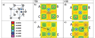
Figure 3. (a) Ball and stick model of the OIS (black sphere) and TIS (blue sphere) sites, (b) and (c) charge density for the TIS for He and H, respectively; (d) and (e) the same for OIS. Labels A–J indicate the atoms in the charge distribution map. For TIS, the A and B atoms interact with H, in addition to the J and E, but for OIS the hydrogen only interacts with J and E. The colour bar shows the magnitude of the charge density.
Download figure:
Standard image High-resolution imageAnother important effect of the impurities is the deformation produced in the metallic bulk. From this point of view, the He atom has a greater impact in the metallic structure. This is especially appreciable in the TIS site. The final volume of the irregular tetrahedron formed by the four W atoms around the light atom increases a 30% in the case of He and only a 12% for a tetrahedral H atom after a complete relaxation. This result implies that, although the He atom does not interact electronically with the W atoms, it is able to create a bigger deformation in the metallic matrix. On the other hand, the stronger electronic interaction of the hydrogen induces a small geometrical deformation in its search to find the most stable accommodation, due to the bonds established among the H and the nearest W atoms.
Therefore, from these results we can conclude that the W basis generated for the SIESTA code has successfully passed the second test.
3.3. H and He inside a vacancy in W bulk
In a nuclear fusion environment, the tungsten samples will be exposed to radiation damage. This implies that an important number of vacancies can be created. Thus, the light He and H atoms can occupy these vacancies present in the material [32]. For this reason, the theoretical analysis of the energetic behaviour of one (or several) light atoms occupying the vacancy appears as a very interesting task. In a first step, the mono-vacancy is created by removing one W atom from the bulk. The first nearest neighbour W atoms approach the vacancy center while the second nearest neighbours are detached from their original positions as analyzed previously [33]. The formation energy obtained with our SIESTA basis is 3.11 eV in better agreement than the previous point defects with the VASP value 3.16 eV (see table 1). Once the vacancy is created, the light atoms (He and H) can be placed inside it. The energies of the calculated configurations are presented in table 2. Hydrogen prefers a sub-octahedral position (S-OIS) out of the vacancy instead of the substitutional site as reported before [34]. The difference in the formation energy between the H in and out of the vacancy is 0.75 eV (see table 2). Notice that the formation energy of the H outside the center of the vacancy for SIESTA is 2.87 eV, close to the VASP value of 2.80 eV. However, in the case of the formation energy for the H atom accommodated in the center of the vacancy, the difference between the VASP and SIESTA values is 0.41 eV. The reason is that SIESTA overestimates the interaction when the H is occupying the vacancy that produces a strong decrease in the formation energy (see table 2). Nevertheless, this configuration is not the most stable for one H atom close to a vacancy and the good agreement found for the H atom outside the vacancy should be highlighted. In addition, other studies have found that the formation and binding energies are consistent with both codes [35]. In this most stable case, the H is placed at 1.13 Å from the vacancy site (see figure 4(a)), a little bit closer than the value obtained in our VASP simulations (1.26 Å), by Liu et al (1.28 Å) [36], Ohsawa et al (1.27 Å) [37] and Jiang et al (1.26 Å) [38]. On the contrary, the He atom moves directly to occupy the position of the absent W atom, whereas the W-He repulsion experiments a strong reduction as explained in [33]. The resulting formation energy obtained by the SIESTA code is 4.70 eV in good agreement with the calculated VASP value (4.75 eV) [15].
Table 2. Formation energy of the vacancy with a H/He atom inside.
| SIESTA (eV) | VASP (eV) | |
|---|---|---|
| 1H1V in/out | 3.62/2.87 | 4.03/2.80 |
| 1He1V | 4.70 | 4.75 |
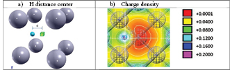
Figure 4. (a) The most stable configuration for one H atom close to a vacancy is shown indicating the distance defined in the text and (b) the corresponding charge density map where the interaction between the H and the central W atom in the nearest cell is shown (see green colour in the map). The red colour indicates the charge deficit around the vacancy.
Download figure:
Standard image High-resolution imageFigure 4(b) shows the valence charge density associated with the S-OIS case. It reflects a lower charge in the center of the vacancy (see the red area in the center) in a similar way as explained before. The symmetry of the red area is broken due to the presence of the H atom. Finally, the green colour can be associated to the W-H interaction among the H and the first metallic neighbours.
The agreement of the energies and charge distribution with the plane wave codes results seems to further validate the W basis proposed for SIESTA in this work. Thus, the basis has positively passed the third test whereby a metallic vacancy is combined with a light atom (H and He).
Consequently, we can conclude that these 3 tests validate our basis to perform the additional calculations proposed in the following sections.
4. Point defects close to the surface
4.1. Formation energy
Once we have analyzed the different defects in the bulk, the next step is to study how they can reach the surface. From this section onwards, all results have been obtained with SIESTA (using the PBEsol functional). According to figure 1, the highest x-ray peak intensity is obtained for an α − W (1 1 0) surface. For this reason, we have firstly simulated a clean W (1 1 0) surface following the conditions described in the methodology section. The analysis of the distance between the first and second layers shows a reduction of 4.3% from the distance between bulk layers, in agreement with the results shown by Nojima et al (4.1%) [9].
After that, we have created a vacancy and a self-interstitial atom at different layers near the surface. Subsequently, an energetic analysis of the stability is performed. Figure 5(a) shows the formation energy for a vacancy with a red curve with diamond points. The relative position of the vacancy with regards to the surface is displayed in figure 5(b). Plane 1 means that the vacancy is at the surface. For plane 2 the vacancy is formed when a W atom is removed from the layer immediately below the surface and so on. The bulk conditions have been recovered when plane 5 below the surface is reached. At this point, the formation energy takes on a value of 3.03 eV, very similar to the one calculated in the bulk, 3.11 eV (see table 1). As expected, the most stable configuration is found when the vacancy is at the surface [8]. There is a big gain of 1.54 eV when the vacancy moves from the second layer (2.68 eV) to the surface (1.14 eV), while moving the vacancy from the second to the fifth layer the energy increases until it saturates close to the bulk value. This behaviour is similar to that presented by Wang et al [39] for a vacancy near the tungsten surface. They report a slight increase in the formation energy with respect to the depth of the vacancy. For them, the formation energy of the vacancy at the surface is 1.85 eV, well above our value (1.14 eV), while for the vacancy in the bulk they obtained a value of 3.07 eV, in good agreement with the one presented in this work (3.11 eV).

Figure 5. (a) Formation energy of a vacancy (red diamonds) and a self-interstitial (black triangles) versus the depth relative to the surface. (b) Ball and stick model of a monovacancy in different layers (from 1 to 5) with respect to the W(1 1 0) surface. (c) The adsorbate configuration found after the relaxation of a self-interstitial starting from the fourth to the first layer. (d) The first stable self-interstitial position located on the fifth plane.
Download figure:
Standard image High-resolution imageThe self-interstitial case presents a different behaviour. When a d111 is created at the surface, the atoms are reorganized in the system that finally recovers the 10-layer configuration with an additional atom adsorbed in a hollow position (see figure 5(c)). When the dumbbell is created from the second to the fourth layer, the system undergoes a strong reconstruction obtaining, at the end of the relaxation, the same structure as for the final reconstruction of the first layer. This suggests that there is no energy barrier for a W atom to find the surface in a crystal without vacancies. This idea is supported by the very small barrier obtained for a d111 moving in the perfect bulk [15, 40]. The formation energy calculated for this configuration is 1.64 eV, similar to the 1.62 eV found by Yang et al [41]. Finally, for the fifth layer, the d111 remains stable as shown in figure 5(d) but the resulting formation energy (8.2 eV) is a much smaller value, comparing to the one calculated in the perfect bulk 10.35 eV (see table 1). This great energy difference reflects that a larger unit cell is required to recover the bulk conditions due to the high deformation created by the extra W in the surrounding atoms. In fact, this situation implies a meta-stable structure, i.e. the calculations have been performed at 0 K temperature and consequently, due to the small energy barrier of the dumbbell, it is expected that a fast movement to the surface should take place when thermal effects are included.
A similar energetic analysis can be done for one H or He atom adsorbed at different layers close to the surface. Firstly, we have checked that the most stable position in each layer is the corresponding tetrahedral site as happened in the bulk. This is confirmed by our SIESTA simulations. In figure 6(a) the formation energy of the most stable cases in each layer is represented for H (green circles) and He (blue squares). At the third, fourth and fifth layers, the most stable sites are the TIS for both H and He, as happened in the bulk [36]. In fact, the H atom is adsorbed on a hollow site (near to the equivalent tetrahedral position) bonded to the surrounding W atoms as happened again in the bulk [8, 9]. The formation energy remains stable close to the bulk value for both impurities until the most stable position is found at the surface (see the schematic representation in figure 6(c)). In fact, for both kinds of atoms, the positions at the second layer are unstable, and thus a direct movement is found to their corresponding superficial more stable positions. The H and He atom present a different behaviour at the surface. While the H atom stays bonded to the superficial W atoms around a hollow position, the He atom is completely desorbed, finding a very stable position more than 3 Å far away from the metallic surface (schematically represented in figure 6(b)). In the latter situation, the system gains more than 6 eV, showing the great repulsion established between the He and the metallic atoms in the bulk as suggested before [33]. Wang et al [39] show the formation energy for He with respect to the position in the W-cell and the depth at which this cell is located. In the plane just below the surface, the He atom is not stable and so they have only shown an unrelaxed value of the energy. However, directly below this second plane, the formation energy is close to the bulk energy (6.15 eV). This result is directly comparable to our calculations as discussed above and agrees with what was shown in figure 6(a). The He atom has the same energy in the first and second planes because the final configuration is the same. In both cases, the He atom escapes from the bulk, while in the third plane He (and H too) atoms begin to behave in a similar way as in the bulk.
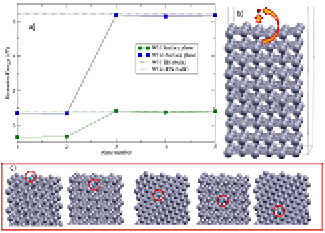
Figure 6. (a) Calculated formation energy for one H atom (green circles) or He atom (blue squares) adsorbed at different layers with respect to the surface. (b) Ball and stick model of the He atom desorbed from the W (1 1 0) surface. (c) Ball and stick model for one H atom in the different layers.
Download figure:
Standard image High-resolution imageSummarizing, the four defects analyzed in this section have a value for the formation energy very similar to the bulk when they are at the fifth layer, except in the case of the SIA, probably due to technical details related with the size of the unit cell used. This means that future calculations involving surfaces will require at least 10 layers to recover the bulk conditions, unless a great deformation could be created (as happened with the additional W atom in the SIA case) and then an even bigger unit cell is highly recommended.
4.2. Charge density for defects at the surface
Now we will analyze the charge distribution in the system when the defects are placed in different layers. We will take the previously calculated bulk as a reference (see figures 3 and 4).
Figure 7(a) shows a frontal view of the clean W (1 1 0) surface. The first neighbour distance is labeled by h, the lattice parameter is i, and finally the distance between the third neighbours to the vacancy is j, as shown in figure 7(a). In figures 7(b) and (c), a red region appears around the vacancy showing the absence of charge. The three parameters h, i, j defined above, are reduced from 2.740 Å to 2.723 Å for h, from 3.167 Å to 3.120 Å for i and from 8.968 Å to 8.880 Å for j, showing the tendency of the metallic atoms around the vacancy to approach its center. Figure 7(d) shows the vacancy in the 5th plane. It can be seen that the red region is symmetrical in comparison with the case of a vacancy located in the first plane.
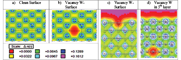
Figure 7. Frontal view of the charge distribution on the (a) clean surface and (b) a vacancy; (c) lateral view of the vacancy at the surface; (d) lateral view of the vacancy in the 5th plane. Again, the green paths indicate the bonds between atoms and the red patch shows the absence of charge. The indexes h, i and j define the first neighbour distance, the lattice parameter and the distance between the third nearest neighbours to the vacancy at the surface, respectively.
Download figure:
Standard image High-resolution imageThe analysis of the deformation when W is absorbed at the surface is shown in figure 8(a). In this case the W adatom is placed at a hollow position at 1.810 Å above the surface. This is in contrast with the bulk value of 2.290 Å, suggesting that the W atom approaches to the surface in order to optimize the bonds (see the darker green colour between the surface and the adsorbed W atom in figure 8(a)). This effect on the adatom has been previously found in other bcc materials such as iron [42], where the distance of an Fe adatom over an Fe (1 1 0) surface is 1.771 Å, while in bulk conditions this distance is 2.035 Å.

Figure 8. Charge density for the three defect atoms on the surface. (a) The W adatom shows a smaller W–W distance. (b) Hydrogen accommodates much closer to the surface in a displaced position with regards to the bulk. (c) Helium accommodates at the greater distance from the surface, interacting therewith only by means of Van der Waals forces. The legend is the same as in previous figures. All previous and current 3D figures and the distribution map of the charge density have been made with XCrysDen [43].
Download figure:
Standard image High-resolution imageIn the same way, the H atom is adsorbed at a hollow position close to the surface layer. The H-surface distance is 1.30 Å, close to the W-surface distance, although far from the bulk value of the distance between the W plane and the H interstitial, namely, 0.7 Å. Hydrogen interacts electronically with W (figure 8(b)) sharing part of its charge with the surrounding W atoms. The total charge of the H adsorbed on the surface is 0.637 e−, larger than the bulk value of 0.440 e−. These results show that H has less charge at the bulk, where H has a greater number of 1NNs to interact with. The deformation between the first and the second layers when the H atom is at the surface is a 1.5% with respect to the pure surface (figure 8(b)) while in the fourth and fifth layers it is a 1.3% with H in the 5th plane (figure 9(b)). On the other hand, the He atom moves more than 3 Å away from the surface. This means that the interaction between He and substrate is weak, taking place via Van der Waals forces (see figure 8(c)), recovering the charge distribution of both isolated systems.
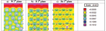
Figure 9. Charge density in a bulk-like environment calculated at the 5th layer for the different defects analyzed. (a) SIA d111, (b) H atom, and (c) He atom.
Download figure:
Standard image High-resolution image
Although the charge deformation produced by the defects is clear, as shown in figure 8, we have not observed signs of reconstruction on the 110 surface, induced by the presence of H, He or a W adatom, just as it is neither seen in the work of Johnson et al and Nojima et al [8, 9], and happens as well with the 100 surface [8].
In figure 9, we show the corresponding charge distributions for the SIA d111 and the light H/He atoms placed at the fifth layer. In the case of the W SIA at the 5th layer (figure 9(a)), it binds to its neighbours and moves the rest of them along the 〈1 1 1〉 direction, producing a dumbbell 111. The charges of both atoms in the dumbbell are −0.054 e− in the bulk and −0.065 e− in the 5th layer, explaining why the formation energy differs in both cases and suggesting that a bigger unit cell should be used.
Regarding the light atoms, hydrogen (figure 9(b)) interacts electronically with the neighbouring metallic atoms that are slightly deviated from their stable lattice positions. The charges of the closest neighbours W are −0.106 e− in the bulk in good agreement with the value −0.108 e− (in average) obtained in the 5th layer. On the other hand, helium (figure 9(c)) does not interact electronically with the metallic neighbours, as shown by the absence of green paths indicating that a bond is not formed. In any case, the He atom produces a charge re-arrangement in the W atoms in its vicinity. The Mulliken charge approximation result shows how the surface generates an asymmetry in the charge rearrangement around the defects depending on the depth (see the supplementary material A1 (stacks.iop.org/MSMS/24/045006/mmedia)).
The interaction with 2NNs and 3NNs changes between the light atom species. H interacts electronically with the 1NNs without inducing any changes in neither 2NNs nor 3NNs. On the other hand, He does not interact electronically with the 1NNs, although it induces charge rearrangements in the 2NNs and 3NNs. Hydrogen in the TIS position displaces W atoms away by a 3.7% (figure 9(b)), while W first neighbours around a He atom are displaced even further by a 6.7% with respect to their position in the bulk. Then, the deformation produced by the He in a TIS position at the fifth plane (figure 9(c)) is greater than that produced by H in both cases in good agreement with the corresponding bulk case.
Finally, we will focus our attention in the intermediate layers. As mentioned before, above the fifth plane the extra W atom produces a cascade of movements along the (111) direction that lead to the appearance of an adatom in the surface, instead of an interstitial in the internal layers. Consequently, there is not any real structure to analyze between the 2nd and the 4th layers. On the other hand, the vacancy and light atoms (H and He) produce a slightly asymmetric density of charge at the intermediate layers. This asymmetry disappears at the fifth layer as shown in figure 9 (a charge analysis can be found at the supplementary material A1).
The average interplanar distances between the layers are almost unchanged when placing a defect on the surface, being the first layer closer to the second than the rest. However, there are certain changes in the arrangement of the layers by introducing a defect in the volume. For instance, the thickness of the slab increases in the case of H by 0.27%, by 1% for a W adatom, by 0.22% for a He, and decreases in the case of the vacancy by 0.13%. Although very low, the deformation induced relates to the observation that high concentrations of defects cause problems that appear as pickling or fracture in NW tungsten [44, 45], causing defects as self-interstitials, vacancies and H and He interstitials to move closer to the grain boundaries where, according to previous studies, they find more stable accommodations [46].
5. Conclusions
In conclusion, a new SIESTA basis has been presented for tungsten. The simulations for the structural properties, bulk and Young's moduli are in good agreement with our experimental measurements. Different defects (a self-interstitial, a monovacancy, a H and a He atoms) have been introduced in the perfect W bulk and the results compare positively with the data calculated with a plane wave code. The great tendency of the four defects to reach the surface has been proven. The self-interstitial migrates directly to the surface from the fourth layer due to the small energy barrier that it has to overcome. Both, vacancy and H atom present a similar behaviour, namely, a great energy gain is obtained when they finally reach the surface. On the other hand, when the He atom reaches the second layer, it directly desorbs far away from the surface. Our results show how the bulk conditions are rapidly recovered at the fifth layer for the different defects, although for H and He a bulk-like behaviour is already found in the third layer. Deformation due to the implantation of H, He, W, or the presence of vacancies reveals itself as an increase in the interplanar distances.
The Mulliken charge analysis performed shows that hydrogen and W atoms stay bonded to the surface atoms while the He atoms do not create any bond with the metallic atoms at any layer. The analysis of the charge distribution and charge exchange shows how each defect evolves from the bulk to the surface. The W adatom and the H at the surface acquire a greater charge than the W and H interstitials in the bulk. In the case of a vacancy at the surface the charge distribution of the neighbours is asymmetrical, recovering the complete symmetry at the fifth layer. Although the helium atom does not interact electronically, it influences the distribution of the lattice charge of tungsten that ends up recovering its bulk configuration at the third layer.
The results obtained with this work could be considered as highly valuable input for subsequent simulations on larger scales, such as kinetic Monte Carlo or Molecular Dynamics.
Acknowledgments
This work has been supported by the Spanish projects MAT2012-38541-C02-01and ENE2012-39787-C06-03 from the Ministry of Economy and Competitiveness. CLG acknowledges the computer resources and technical assistance provided by the Centro de Supercomputación y Visualización de Madrid (CeSViMa) and Prof E Bringa for his extensive help in the discussion of some results. CG and RI thank the FP7 project 'RADINTERFACES' the RES project FI-2014-3-0005 and the European PRACE-3IP project (FP7 RI-312763) resource Fionn based in Ireland at ICHEC and Supernova based on Poland at Wroclaw University of Technology Research. NG work is supported by MINECO (Spain) under project JCI-2012–12652.