

Abstract
A range of methods including soft lithography are available for patterning protein layers for cell adhesion on quasi-planar substrates. Suitably structured, these layers favor the geometrically constrained, controlled growth of cells and the development of cellular extensions on them. For this purpose, the ability to control the shape and dimension of cell-adhesive areas with high precision is crucial. For more advanced studies of cell interactions, the surface modification or functionalization of substrates with complex topographies is desirable. This paper describes a simple technique allowing to produce surface modification patterns using delicate molecules such as laminin on substrates exhibiting pronounced topographies with recessed and protruding microstructures. The technique is based on the combination of sacrificial photoresist structures with a connected parylene-C layer. This layer locally adheres to the substrate wherever the substrate needs to be protected against the surface modification. After surface modification, the parylene-C layer is peeled off. Patterns comprising arbitrary networks of modified and unmodified substrate areas can thus be realized. We demonstrate the technique with the guided growth of neuron-like PC12 cells on networks of laminin lines on substrates structured with micropillars and microwells.
Export citation and abstract BibTeX RIS
1. Introduction
The analysis of cell–cell interactions and the arrangement of cells into networks of controlled geometry has grown rapidly over the past decade and stays important for biological studies and biomedical research. Positioning individual cells has become a key technique for cell engineering applications such as cell therapy and brain regeneration [1]. Various techniques relying on microfluidic guiding structures [2, 3] and traps [4, 5], field-induced dielectrophoresis [6], mechanical constraints [7] and surface modification [8] by, e.g. chemical treatment [9] have been used to position and fix cells in intended locations.
The current state of the art in chemical surface modification relies on soft lithography [10–12]. By means of micro- or nanostructured elastomeric material stamps, layers of molecules are transferred in well-defined patterns onto planar substrates. Micro-contact printing is the most widely used soft lithography variant [11], where a patterned polydimethylsiloxane (PDMS) master stamp is used to transfer a thin layer of a chemical species self-assembled on its surface by direct contact onto the planar target substrate [12, 13]. When nanometer-sized features are involved, the technique is called nano-transfer printing [14, 15]. Microfluidic channels in PDMS filled with solutions carrying the surface-modifying species [16] and laminar flow configurations with more than one such species [17] have also served the purpose of controlled surface modification. Besides these soft lithography based techniques, other methods relying on ion implantation [18], laser photo-ablation [19], photolithography [20] and laser vapor deposition [21] have also allowed to realize patterned surface modifications. However often they require complex cleanroom facilities.
None of the techniques mentioned so far allows to produce arbitrary surface modification patterns on substrates with pronounced topographies. Although Langmuir–Blodgett films [22] can readily be deposited over large areas and on high-aspect-ratio microstructures [23], it is challenging to structure them into micrometer-scale patterns and constrain their deposition to small areas.
An alternative material able to cover surfaces with pronounced topographies is parylene-C. By chemical vapor deposition, this poly(p-xylylene) polymer is known to conformally envelop complex, high aspect-ratio microstructures [24]. Moreover it is appreciated for its chemical barrier properties [25] and moderate cost. Structured parylene-C layers have been peeled off from planar substrates [26] and more complex surfaces [27]. Several studies have demonstrated the use of the parylene peel-off technique to pattern proteins [26, 28, 29]. However this technique has served to realize only simple geometries consisting of isolated surface-modified patches without interconnections, since it is most advantageous to peel off the parylene-C protection layer when it is a single connected layer.
For advanced studies of cell interactions, the preparation of arbitrary surface modification patterns on surfaces with pronounced topographic features is desirable [30]. To the best of our knowledge, none of the above techniques is able to achieve this goal when the surface modification relies on delicate organic molecules such as proteins. These are incompatible with the solvent-based development and cleaning procedures of standard microfabrication. In this paper, we propose a solution to this problem based on a parylene-C protection layer shaped by sacrificial photoresist structures. After completion of the process the high-topography surface possesses the altered property in the intended areas.
The technological elements of this concept were succinctly reported in a previous conference publication [31]. Here we describe the technique including its potential and limitations in significantly greater detail. This includes the fabrication and systematic analysis of a wider range of surface topographies and surface modification patterns.
2. Materials and methods
2.1. Concept
The concept of this technique relies on the selective protection of the surface by parylene-C [26]. Areas intended to remain unmodified are protected by parylene-C while the complementary areas are left unprotected by it. After surface modification of the unprotected areas the parylene-C protection is simply peeled off [28].
Although this procedure may seem trivial, we give it a twist that allows a much larger variety of patterns to be realized than using the conventional technique. Conventionally parylene-C is deposited conformally on the entire substrate [32]. It is then structured by photolithography and etching. For topological reasons, however, a wide class of surface modification patterns cannot be realized in this way. Consider the example of an unmodified island completely surrounded by an area with modified surface properties. The corresponding parylene-C layer would need to be structured into the corresponding island geometry and, after surface treatment of the substrate, would need to be peeled off. This is impracticable if the island is small or one among many islands isolated from each other by the surface-modified area. The parylene protection layer can then be peeled off in a single step only if it is connected. However, the islands would then cease to be isolated, in contradiction with the original goal.
The central innovation introduced by this paper is to implement the connection idea in such a way that the isolation of individual parylene-protected areas on the substrate remains guaranteed. For this purpose we propose to raise the connections between these areas above the substrate surface. In this way the surface modification chemistry is able reach the entire area intended to be modified. As illustrated in figure 1, this general concept can be applied even to substrates with pronounced topography including recesses and protruding microstructures. More specifically, figure 1(a) schematically shows a substrate with a recess and two areas with protruding pillars. As schematically shown in figure 1(b) the goal in this schematic example is to modify the surface properties of the recess, of the pillar array in the middle, and partially of the extended pillar array on the right. In this fictive geometry, unmodified patches are surrounded by a modified area. The corresponding parylene layer geometry is shown in figure 1(c) in a top view and in cross-section. Portions of the parylene are raised above the surface by vertical parylene walls anchored on the substrate in areas protected by parylene. After surface modification of all exposed substrate and parylene surfaces, the parylene layer is peeled off in a single piece (figure 1(d)); as a result, the substrate is locally modified as intended and as indicated by the surface portion in green color in figures 1(b) and (d)–(g). Using a second surface modification process, the complementary area can now be modified to assume a second surface property. This is indicated in figures 1(e)–(g) by the red surface coloring. The contrast between surface modification no. 1 and surface modification no. 2 therefore enables patterned cell adhesion and growth, as indicated by figures 1(f) and (g) and demonstrated in section 3.

Figure 1. Concept of the parylene-C-based surface modification of substrates with pronounced topographies. (a) Substrate comprising recessed and protruding microstructures in top view and cross-section. (b) Green color indicates areas including recesses and protruding microstructures destined to be surface-modified by process no. 1, while the complementary area is to be protected against surface modification. (c) Parylene-C is deposited so that areas to be protected are covered by parylene, whereas in complementary areas the parylene layer is raised sufficiently above the substrate surface; unprotected substrate areas are ready to be surface-modified through openings in the parylene layer. (d) Surface modification process no. 1 and removal of the parylene protection layer by peel-off. (e) Optional surface modification process no. 2 to modify complementary areas previously protected against the first modification process. All cross-sections are along line A–A' in (a). Cell growth is favored on areas with surface modification no. 1 and suppressed on complementary areas with surface modification no. 2.
Download figure:
Standard image High-resolution image2.2. Substrate fabrication
In order to validate the concept and test its limits, substrates with pronounced topographies were fabricated. Microwell and micropillar arrays of various in-plane geometries and sizes and out-of-plane dimensions were realized on two-inch standard  silicon substrates. Silicon microstructures were fabricated using photolithography (using Shipley resist S1805) followed by deep reactive ion etching (DRIE). Standard DRIE with an RF coil power of 600 W and RF platen power of 17 W gives typically an etching rate of 3 µm min−1 with a scalloping of 300 nm per cycle. For each cycle, the isotropic etching and passivation times are 13 s and 7 s respectively, while the chamber pressure during the etching step is around 30 mT. Those conditions promote the isotropic etching of silicon with high-density plasma because of the large average adsorption time of ions on silicon (13 s) and the non-directional etching due the relatively high pressure.
For this study, the DRIE recipe was modified in order to reduce the scalloping while keeping accurate depth control and vertical sidewalls. The strategy was to reduce the chemical contribution to etching by lowering the plasma density (coil RF power of 300 W) to get fewer active chemical species, by increasing the physical contribution of ions by raising the platen RF power to 30 W and decreasing the chamber pressure to 5 mT to reduce the rate of ion collisions and thus benefit of a more directional etching. After optimization of the recipe by lowering the etching/passivation times to 7 s/4 s, the resulting etching rate is about 1 µm min−1 with a scalloping of less than 100 nm, with almost vertical sidewalls for etch depths ranging from 1 µm to 7 µm. Aspect ratio dependent etching was not investigated due to the relatively large periods of the pillar arrays. After DRIE, photoresist residues were removed by O2 plasma.
Different geometries were realized in order to allow the influence of topography on the surface modification process to be assessed. In view of a first study, patterns of proteins favoring cell attachment were designed to cover surfaces with pronounced topographies, with the parylene-C layer anchored exclusively on planar substrate areas. Consequently these planar areas remain unfavorable for cell growth. The structured areas to be surface modified were designed to comprise microwells [33, 34] and micropillar arrays [4, 35]. Circular microwells with a diameter of 40 µm and depths of 5 µm and 10 µm (figure 2(a)) were produced. The micropillar arrays are composed of 19 pillars in a hexagonal arrangement (figure 2(b)) with a pitch between neighboring pillars of 5 µm. Pillars with diameters of 500 nm–900 nm and heights of 3 µm, 5 µm, and 7 µm were realized. Both, microwells and micropillar arrays were arranged in the simplest periodic patterns in two dimensions, namely hexagonal and square lattices with periods of 60 µm and 150 µm, respectively.
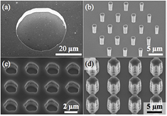
Figure 2. Scanning electron micrographs of silicon substrates with examples of recessed and protruding microstructures to be surface-modified using the parylene-C protection layer method: (a) microwell (diameter 40 µm, depth 5 µm); (b) array of 19 micropillars (diameter 1 µm, height 5 µm); section of extended square arrays of (c) microwells (depth 5 µm) and (d) micropillars (height 7 µm).
Download figure:
Standard image High-resolution imageThe second study aimed at assessing the suitability of parylene-C in protecting complex extended topographies against the surface modification process. For this purpose, large areas of the substrates were structured with high-topography features. The parylene layer was then designed to partially protect these areas, while leaving others free for surface modification. On the one hand extended regular arrangements of microwells were etched, with well diameters of 2 µm, 5 µm and 10 µm and a depth of 5 µm (figure 2(c)). On the other hand we also fabricated micropillars with nominal diameters of 1 µm, 3 µm, and 5 µm and heights of 3 µm, 5 µm, and 7 µm forming square lattices with nominal distances between next neighbors of 1 µm, 3 µm, and 5 µm. Depending on the local chemical contribution of the etching step, the shape of the smaller micropillars was found to depart from the exact, circular geometries defined by the mask (e.g. figure 2(d)). Each configuration was designed to cover an area of 1 cm2.
2.3. Parylene protection layer fabrication
The process steps leading to parylene-C protection layers with the required properties are summarized in figure 3. The starting point is again a substrate that may comprise protrusions and recesses, as shown in figure 3(a). Areas to be surface modified are first protected using a sufficiently thick, photolithographically structured, sacrificial photoresist layer (figure 3(b)) [36]. Since the test microstructures in this work are up to 10 µm deep and 7 µm high, we worked with 10 µm thick AZP4620 photoresist. A 10 µm thick parylene-C layer (from Specialty Coating Systems, Indianapolis, USA) is then conformally deposited. At this thickness, the layer and in particular its more fragile sidewalls proved to be robust enough to survive the mechanical strain during peel-off. In preparation of the parylene patterning, an approximately 50 nm thick aluminum (Al) mask is sputtered onto the structure and Shipley S1818 photoresist (figure 3(c)) is spun on using the standard recipe for 1 µm nominal thickness. After the resist has been photolithographically exposed, both resist and Al layer are locally removed in a single step using 2.38% tetramethyl ammonium hydroxide (TMAH) developer (Tama Chemicals Co., Ltd, Japan) (figure 3(d)). Anisotropic RIE is then used to cut through the parylene-C, as shown in figure 3(e). During this step, the S1818 photoresist is also removed, whereas the Al layer assumes the function of a reliable mask. Next, the sacrificial photoresist is dissolved in acetone (figure 3(f)). Although the Al layer serves no further purpose, it is left on the parylene-C since its removal would require unnecessary additional processing. Finally an oxygen (O2) plasma treatment removes solvent and photoresist residues and makes the parylene hydrophilic. The structure is then ready for surface modification.
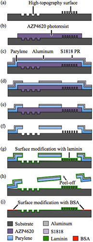
Figure 3. Fabrication process for parylene-C-based surface modification: (a) substrate with pronounced topography; (b) structuring of sacrificial photoresist; (c) deposition of parylene-C and Al, spinning of photoresist; (d) photoresist, Al, and (e) parylene structuring; (f) sacrificial photoresist removal; (g) surface modification no. 1 with laminin; (h) parylene protection layer removal; (i) surface modification no. 2 with BSA.
Download figure:
Standard image High-resolution image2.4. Surface modification
With the purpose of promoting the controlled attachment and growth of cells, the cell-adhesion-promoting protein laminin is then dispensed in phosphate-buffered saline (PBS) solution (ten times diluted Dulbecco's PBS 10×, D1408, Sigma-Aldrich), densely covering all exposed parylene-C and substrate surfaces, as shown in figure 3(g). After rinsing, the parylene layer is peeled off the substrate, as schematically shown in figure 3(h), using a pair of tweezers. As a result the initially photoresist-covered areas on the substrate are exclusively modified.
For visualizing the surface modification patterns with the purpose of controlling their geometry we employed a mixture of 25% of rhodamine-tagged laminin (LMN01-A, Cytoskeleton, Inc.) and 75% laminin (L2020, Sigma-Aldrich) with a total laminin concentration of 50 µg ml−1 [37]. Fluorescence microscopy (Olympus IX, Olympus) was used to detect rhodamine-tagged laminin using its excitation and detection peaks of 535 nm and 585 nm, respectively. Alternatively laminin-coated areas can also be distinguished from laminin-free areas after optimizing the contrast of optical micrographs.
In view of obtaining patterned cell cultures, after laminin coating and parylene-C peel-off the substrates are exposed to a 5%-solution of bovine serum albumin (BSA) (A-7906, Sigma-Aldrich) [38] in PBS for 2 h. During this exposure, the complementary area formerly protected by parylene is BSA-coated, as shown schematically in figure 3(i). Cell growth is favored on laminin and suppressed on BSA [39].
2.5. PC12 cell culture
The experiments were performed using PC12 cells (RCB0009, Riken Bio Resource Center) that had undergone fewer than ten passages with Dulbecco's Modified Eagle's Medium (DMEM) (D5796, Sigma) supplemented with 1% (v/v) penicillin-streptomycin (P4333, Sigma), 10% (v/v) fetal bovine serum (Biosera), and 10% (v/v) horse serum (Japan Bio Serum). Neuron-like PC12 cells were seeded as described previously [40, 41] onto laminin-coated chips with DMEM supplemented with 1% penicillin-streptomycin and 10 ng ml−1 nerve growth factor (N6009, Sigma). About 30 000 cells cm−2 were deposited onto the chips. Incubation was carried out under standard conditions for neuron-like PC12 cells, i.e. 5% CO2 at 37 °C. For seven consecutive days, the medium was left unchanged. This duration was required for the development of cellular extensions. In this study, we do not explicitly distinguish between axons and dendrites and subsequently term all extensions neurites.
After observation by optical microscopy (Olympus IX, Olympus), neuron-like PC12 cells were visualized with the LIVE/DEAD® Viability/Cytotoxicity Kit for mammalian cells (L3224, Molecular Probes). In this test, viable cells are labeled with calcein AM detectable as green fluorescence, whereas dead cells are labeled with ethidium homodimer (EthD-1) responding by red fluorescence. Excitation of the live stain occurs at 494 nm with fluorescent emission at 530 nm. For the dead stain, the excitation is at 528 nm, with fluorescent emission at 617 nm.
3. Results
3.1. Planar laminin structures
First, we explore the limits of the new process on planar substrates. Of interest are the minimum diameter of laminin islands and the minimum width and maximum length of laminin lines.
As far as islands are concerned, we obtained well-controlled protein patches with diameters down to 600 nm. For these experiments, the parylene layer as specified in section 2.3 was RIE-patterned in planar areas, without the use of sacrificial photoresist, using an Al mask with square and circular holes with diameters down to 1 µm. At the smallest dimensions, both types of openings in the Al mask similarly resulted in circular protein-coated areas due to the high aspect ratio of the holes etched through the parylene (1 µm : 10 µm).
Regarding the achievable line geometries, we successfully patterned microchannels with widths between 1 µm and 100 µm. Since the traces defined by the microchannels are usually intended to connect other areas with modified surface properties, sacrificial photoresist protection was used in this case. Figure 4 shows the entrance ports of microchannels of selected widths ranging through the entire investigated range as well as laminin traces of corresponding dimensions after parylene removal. It is remarkable that the parylene layer reliably spans even the widest channel. The regularity of the laminin traces suggests that the channels were successfully cleared of their sacrificial photoresist.

Figure 4. Scanning electron micrographs of laminin lines of nominal widths (a) 100 µm, (b) 10 µm and (c) 1 µm realized using microchannels of corresponding width in parylene left by sacrificial photoresist. Left hand side: entrance ports of microchannels. Right hand side: top views of laminin lines.
Download figure:
Standard image High-resolution imageNevertheless clearing channels longer than 1 mm proved challenging. For this reason we equipped long microchannels with an opening through the parylene cover every 1 mm of channel length. Through these openings the photoresist is removed effectively from the adjacent channel segments. We report surface-modified lines with an overall length up to 2.5 cm. It proved helpful to ensure the hydrophilicity of the parylene layer by an O2 plasma treatment for reliably filling microchannels of all investigated widths and lengths with aqueous solutions. During the entire process the parylene layer remained firmly attached to the substrate.
The path to more complex surface modification geometries is shown in figure 5. The modification pattern is a hexagonal, honeycomb-shaped configuration of laminin-coated disks connected pairwise by lines (see figure 5(a)). Figure 5(b) shows the corresponding sacrificial photoresist pattern. The structured parylene-C layer after sacrificial photoresist removal is shown in figure 5(c). It consists of dome-shaped reservoirs with an inner diameter of 50 µm and a circular opening at their top, and connected by 10 µm wide microchannels. Figures 5(d) and (e) show scanning electron and fluorescence micrographs of the resulting laminin pattern whose geometry is as intended and whose dimensions are designed to host neuron-like PC12 cells and their interconnection by neurites.
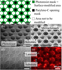
Figure 5. From mask design to a completed surface modification pattern consisting of a honeycomb-shaped arrangement of interconnected disks. (a) Mask geometries for sacrificial photoresist (green) and parylene-C openings (black). Scanning electron micrographs of (b) sacrificial photoresist and (c) parylene-C domes opened at the top and connected by microchannels. (d) Laminin pattern after coating and parylene peel-off. (e) Optical micrograph of laminin fluorescence. All scale bars are 40 µm in length.
Download figure:
Standard image High-resolution imageClearly, similar results on planar substrates can also be obtained by micro-contact printing. However in contrast, the present method can also be applied to substrates with high-aspect ratio microstructures, as demonstrated in section 3.3. Note also that deposition of a parylene-C layer directly on the substrate and its structuring into the intended protection pattern would have led to a large number of separate microscopic parylene-C patches difficult to peel off.
3.2. Parylene peel-off from surfaces with pronounced topographies
The reliable removal of the parylene protection layer from the substrate is essential for the success of the method. Especially on surfaces with fragile microstructures this is not necessarily evident. For this reason, we investigated the peel-off of parylene from substrates densely covered with micropillars of the geometries described in section 2.2. As illustrated by figure 6, the parylene-C layer is able to fully cover the pronounced topography defined by micropillars and can be entirely detached from them. In this case, a 10 µm high and 20 µm wide sacrificial photoresist structure was additionally designed to realize a channel in the parylene and, ultimately, a surface-modified trace on the substrate, as schematically shown in figure 6(a). The micropillars are 5 µm high. After laminin coating, the parylene was peeled off. A scanning electron micrograph during this process is shown in figure 6(b). On the one hand the array of holes in the parylene indicates that parylene has nicely surrounded the micropillars. On the other hand, despite the possibly large mechanical load due to the peel-off, the micropillars remained intact on the substrate. Moreover the bottom view of the channel in the parylene sheet suggests that the channel has been successfully cleared of photoresist through the opening provided for this purpose.
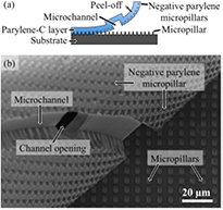
Figure 6. (a) Schematic and (b) scanning electron micrograph of parylene-C sheet deposited on substrate with extended micropillar array during peel-off. The parylene layer comprises a microchannel with an opening and the negative mold of the micropillars from which it has been detached.
Download figure:
Standard image High-resolution imageThe study also showed that some designs are less favorable for parylene peel-off than others. Indeed, figure 7 summarizes the peel-off results as a function of the micropillar geometry characterized by the pillar diameter and height (=substrate etching depth) and the nominal pillar-to-pillar spacing. The quality of the peel-off is measured in terms of the fractional area from which the parylene was clearly removed. The evaluation was performed by optical observation, which allowed to identify, delimit, and quantify areas with imperfect parylene peel-off. Several trends can be inferred from the observations. First, pillars with smaller diameters, smaller heights, and larger spacings ensure an easier release of the parylene. In less favorable cases defined by the pillars with the largest diameter, larger heights and smaller spacings, it was difficult to achieve consistent peel-off because of the rupture of the parylene layer. At the other extreme, the most fragile micropillars with a diameter of 1 µm and a height of 7 µm were found to remain firmly embedded in the parylene upon peel-off. These micropillars broke at their bases and stayed trapped in the polymer matrix.

Figure 7. Quality of parylene peel-off from substrates with extended micropillar arrays as a function of micropillar geometry. Geometry parameters are: micropillar height = substrate etching depth (3 µm, 5 µm, 7 µm), micropillar diameter (1 µm, 3 µm, 5 µm), and nominal spacing between nearest neighbors (1 µm, 3 µm, 5 µm).
Download figure:
Standard image High-resolution imageIn contrast to the parylene-C peel-off from micropillar arrangements, its peel-off from regular well arrangements was found to be unproblematic for all investigated geometries. In fact, we observed no fracture of any microstructure nor rupture of the parylene-C protection layer (see figure S1 of the supplementary information (stacks.iop.org/JMM/26/095017/mmedia)).
3.3. Cell growth
In order to assess the capability of the surface modification technique with regard to controlled cell growth, all three types of substrates exhibiting planar, recessed and protruding topographies were subjected to the cell culture protocol of section 2.5 after selective laminin and BSA patterning.
The tests with planar substrates served for the validation of the basic principle and as a reference for the tests on structured substrates. Results are reported in the supplementary information, in particular in figure S2.
For testing the method on topographies with recesses, we used the microwell geometries described in section 2.2. The surface modification pattern was designed to favor cell attachment and growth within microwells and neurite growth in-between. Patterns similar to those applied to the planar substrates were used: all microwells are coated with laminin and connected by 5 µm wide laminin traces. The complementary areas were again BSA-functionalized. Figure 8(a) demonstrates that the parylene-C peel-off technique works satisfactorily on recessed structures. The wells in figure 8(a) are 40 µm in diameter and have a pitch of 60 µm. Several wells host cell bodies and neurites are seen to protrude across the planar substrate from well to well, essentially along the invisible 5 µm wide laminin lines. In figure 8(b) the wells are 40 µm in diameter and likewise bridged by 10 µm wide laminin traces. A large fraction of cells seem to prefer adhering and growing on the lines. Similar observations were made on this surface modification pattern irrespective of whether the microwell depth was 5 or 10 µm.
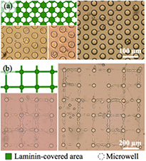
Figure 8. Ordered cell growth on microwell-structured substrates. Schematic topography and surface modification patterns and optical micrographs of cell cultures on (a) hexagonal and (b) square arrangements of laminin-coated microwells connected by laminin lines. Cell adhesion and neurite extension occurs dominantly on laminin structures.
Download figure:
Standard image High-resolution imageIn the case of protruding microstructures, arrangements of clustered micropillar arrays and densely micropillar-covered substrates were used. Using the first category of structures, we validated the possibility to position neuronal cells on micropillar arrays and to guide neurites on pre-defined protein paths between them. Designs with different geometries as described in section 2.2 were tested. The micropillar cluster arrays as well as 5 µm wide paths between them were again coated with laminin. Figure 9 shows the result of cell culture on these patterns. In figure 9(a) cells are seen to populate the asperities offered by the micropillars and to project extensions along the laminin traces connecting the micropillar patches. In figure 9(b) cell somas apparently settled and developed on the connecting lines as well. This growth pattern is confirmed by epifluorescence microscopy (figure 9(b), right hand side) with the live/dead test described in section 2.5.
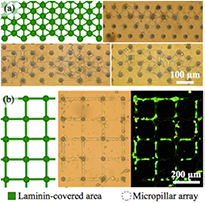
Figure 9. Ordered cell growth on micropillar-structured substrates. Each micropillar array is composed of 19 micropillars in a hexagonal arrangements favoring cell attachment. Schematic geometry of topography and surface modification patterns and optical micrographs of cell cultures on (a) hexagonal and (b) square arrangements of laminin-coated micropillar arrays connected by laminin lines. The right figure in (b) shows the epifluorescence of the culture in the central figure after live/dead cell testing.
Download figure:
Standard image High-resolution imageThe settling and growth of individual cells on alternative surface modification geometries provided for this purpose, both on substrates with recesses and protrusions, is reported in the supplementary information.
Observations of cell growth were made at the boundaries of protruding and recessed structures by optical and scanning electron microscopy. In the case of protruding microstructures, cell bodies were found to cling to their edges. The smaller is the distance between micropillars, the more frequently neurites are found to be attached to the top of the micropillars. In the case of recessed microstructures, cells and neurites tend to stay on the substrate surface rather than descending into the microwells if the well diameters are small. In the contrary, when cells are smaller than the well diameters, they grow also in the wells and in fact mostly along their sidewalls. For the largest microstructures of both types, neurites are found to follow the laminin traces whatever the topography.
4. Discussion
With this study, we demonstrated the possibility to define a contrast between laminin and BSA patterns even on surfaces with pronounced topographies and to guide the adhesion and interconnection of neuron-like cells on them. The design freedom offered by the new method likely allows to realize geometries suited for a wide range of cell interaction studies.
Surfaces with fragile microstructures are not in all cases surface modified as desired. This was found to be the case for example with 1 µm diameter micropillars with aspect ratios of 1:7, irrespective of their spacing. These microstructures were consistently found to break during parylene peel-off and to remain embedded in the polymer layer.
On the technological side, let us note that the Al sputtering has to be carried out with circumspection. Insufficient Al coverage of the parylene sidewalls was found to lead to fracture of the parylene layer during peel-off and thus to its incomplete removal. The reason is simple: subcritical Al deposition leaves microscopic openings along the steep parylene sidewalls where the walls vertically merge into the horizontal portions of the parylene sheets. During parylene etching these openings were found to propagate into the parylene layer and to noticeably weaken it. Isotropic Al sputtering helps to avoid the unwanted openings.
After peel-off we successfully re-used honeycomb-shaped parylene-C protection layers up to four times on planar substrates. For this purpose, a peeled-off protection layer is thoroughly cleaned with isopropyl alcohol and applied to the next substrate, which was previously activated by an O2 plasma. The parylene layer is dried directly on the substrate on a hotplate at 120 °C for 5 min and in vacuum for 20 min. The substrate is then ready for surface modification. Resulting surface modification patterns have served up to four times for culturing patterned cell arrangements [42].
This paper demonstrated the growth of neuron-like PC12 cells on such patterns. However as shown for example by the square matrix design in figure 9(b), neuron-like PC12 cells turned out to be located not only on micropillar arrays at the intersections of the laminin grid, but also on the 10 µm wide connection lines between neighboring micropillar arrays. Therefore if growth is to be achieved exclusively on the micropillar arrays, thinner connection lines are likely preferable. In some cases we even observed the parallel growth of neurites distant by 10 µm along the 10 µm wide lines. This effect likely results from the higher concentration of laminin along the edges of the parylene mask [43], which attracts the neurites. Likely the effect can be reduced with connection lines of smaller width. Finally, we also observed the occasional non-specific cell adhesion on BSA-covered areas close to the laminin coatings. Although BSA reduces such non-specific cell adhesion, it is not able to suppress it completely. Likely non-specific adhesion is promoted by the proximity of large numbers of healthy cells on the laminin patterns. The proximity and number of nearby laminin patterns as well as the growth of neurites on the laminin patterns also seem to be factors in guiding the cell growth in unexpected areas.
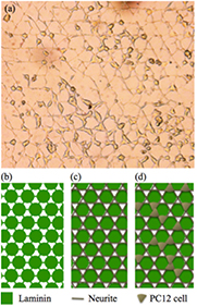
A striking example of such unexpected, yet regular growth is given by figure 10(a), while an interpretation of the culture development is offered in figures 10(b)–(d). Rather than growing from laminin disk to laminin disk strictly along the laminin paths, neurites seem to have favored in this case to grow from disk edge to disk edge via laminin interconnections. Thereby they also form rather straight lines. Triples of such intersecting neurite lines define small triangles which seem to form a basis favorable for cell settlement, despite the BSA on the surface underneath [39]. We conclude that the relation between surface modification pattern and cell culture geometry is more complicated than expected. It is not necessarily the simple geometrical replica of the pattern, but appears to be shaped by additional neurite and cell growth principles that necessitate further study.
Figure 10. (a) Optical micrographs of neuron-like PC12 cells after 5 d of culture on laminin honeycomb pattern schematically shown in (b). Schematic arrangement apparently favored in this case by (c) neurites and (d) cell somas.
Download figure:
Standard image High-resolution image
5. Conclusion
In this paper, a technique for patterning delicate surface modification layers on surfaces with pronounced topographies has been reported. The technique is based on the peel-off of a parylene-C protection layer conformally deposited on a structured sacrificial photoresist. The parylene layer serves the combined purpose of a mask and a structural material: on the one hand it locally protects the substrate by direct contact; on the other hand, by bridging over areas to be surface modified, it interconnects all protection patches into a continuous layer. The substrate is ready for surface modification as soon as the sacrificial photoresist has been dissolved. Thereafter, the parylene layer is straightforwardly peeled off. We demonstrated this technique with the guided growth of neuron-like PC12 cells on different laminin/BSA patterns on planar substrates and others structured with micropillars and microwells of various dimensions and configurations.
The technique promises to be useful for a number of applications including cell biology, microfluidics, and lab-on-a-chip systems. It may also be of interest for applications where surface modification needs to be carried out right before use. It is indeed conceivable that the surface modification chemistry is applied and the parylene layer is peeled off just when needed.
Acknowledgments
This research was funded by the EU 7th Framework Programme under the EUJO-LIMMS project, grant agreement no. 295089.