

Abstract
We present waveguide-integrated graphene devices for photonic gas sensing. In a gas environment, graphene's conductivity is changed by adsorbed gas molecules which serve as charge-carrier donors or acceptors. To accurately probe gas-induced variations in the graphene's conductivity, we optimize the graphene's Fermi level and spectral region. Then, we propose graphene-on-silicon and graphene-on-germanium suspended membrane slot waveguides in which propagating light in the waveguide has a strong interaction with the top graphene layer. The gas concentration can be calculated by measuring the spectrum of the optical reflection from the waveguide Bragg grating. The maximum sensitivity of the waveguide-integrated gas sensor can reach one part per million for sensing gaseous nitrogen dioxide. Its sensitivity is about 20 times higher than that of the graphene-covered microfiber sensor and is comparable with that of a graphene plasmonic sensor. The fabrication of the proposed graphene device is CMOS compatible. Our results pave a way for chip-integrated sensitive photonic gas sensors.
Export citation and abstract BibTeX RIS
1. Introduction
Compact and smart gas sensors have widespread applications in toxic and flammable gas detection, greenhouse gas monitoring, and breath analysis for disease diagnosis. Over the last few decades, a number of gas sensors have been proposed, such as electrochemical gas sensors [1], field effect transistor gas sensors [2, 3], and photonic gas sensors [4–9]. Among them, photonic gas sensors have the merits of high sensitivity, stability, chemical specificity, and electromagnetic immunity compared with other types. Several configurations of compact photonic gas sensors have been proposed and demonstrated, such as microfiber sensors [4], surface plasmon resonance sensors [5], and planar waveguide-integrated sensors [6–9]. Taking advantage of today's cutting-edge fabrication process in microelectronics, silicon waveguide-integrated photonic gas sensors [6–8] have a promising potential to be commercialized at low cost. Such gas sensors may further be integrated with electronic devices for signal processing and communication.
Graphene plays an important role in the development of gas sensors. Graphene is a two-dimensional monolayer of carbon atoms with unique optoelectronic and mechanical properties, high surface-to-volume ratio, and large gas-adsorption capacity. Due to its low carrier density, graphene's conductivity can be changed drastically by adsorbed gas molecules which serve as charge-carrier donors or acceptors to modulate the local carrier concentration of graphene [2, 10]. The variation in graphene's conductivity can affect the electrical and optical performance of devices which can be used to develop electronic and photonic gas sensors. Compared to electronic gas sensors, photonic gas sensors are known to be less affected by the degradation of graphene's quality over time [11]. However, the variation in graphene's conductivity is difficult to optically probe due to the weak interaction between the atom-thick graphene layer and normal incident light. To overcome this limitation, several types of in-plane interaction configurations of propagating light with the top graphene layer, such as graphene-integrated fibers, surface plasmon devices, and waveguide devices, provide a promising platform for developing photonic gas sensors.
In recent years, the development of graphene-based photonic gas sensors has attracted much attention [11–15]. For example, graphene-covered microfiber gas sensors based on Mach–Zehnder-interferometric devices and Bragg gratings have been proposed and demonstrated [12, 13]. A factor of 10 higher sensitivity has been achieved with the sensors than microfiber Bragg grating sensors without any coating [12]. In a recent study, the performance of graphene-based plasmonic gas sensors have been theoretically optimized at low THz frequencies [14]. While these pieces of work have opened a window onto the development of sensitive low-cost photonic gas sensors, it is required to monolithically integrate the gas sensors with other components such as spectrometers and photodetectors before using them as practical devices. Although waveguide-integrated spectrometers and optoelectronic devices have been demonstrated [16–20], the development of waveguide-integrated graphene devices for photonic gas sensing is still in its infancy.
In this paper, we present a systematic design of waveguide-integrated graphene devices for gas sensing. First, we investigate and optimize graphene's Fermi level and spectral region for the purpose of gas sensing. We then propose graphene-on-silicon (GoS) and graphene-on-germanium (GoG) suspended membrane slot waveguide (SMSW) configurations for enhancing the interaction of propagating light in the waveguide with the top graphene layer at mid-infrared (mid-IR) wavelengths such that the light experiences a large phase shift when gas molecules are adsorbed on the top graphene layer. The phase shift results in a variation in the bandwidth of the waveguide Bragg grating. The gas concentration can be calculated by measuring the bandwidth of the waveguide Bragg grating. Our theoretical results indicate that the sensitivity of the proposed gas sensor can reach one part per million (ppm) which is about 20 times higher than that of the graphene-covered microfiber gas sensor and is also comparable with that of theoretically proposed graphene plasmonic sensors.
2. Graphene's relative permittivity
2.1. Graphene's relative permittivity in vacuum
Graphene's optical properties can be determined by its relative permittivity. The equivalent in-plane component of graphene's relative permittivity is given by [20, 21]

where  is the thickness of the graphene layer (0.7 nm in our calculation),
  is vacuum's permittivity,
  is the optical frequency, and
  is graphene's optical conductivity. By using the Kubo method, we can calculate the optical conductivity
  which consists of its intraband
  and interband
  contributions [22]

where


Here,  μS is the universal optical conductance,
  is the Fermi level of graphene,
  is Planck's constant, and Γ1 = 8.3 × 10¹¹ s−1 and Γ2 = 1013 s−1 are relaxation rates at room temperature associated with the interband and intraband transitions, respectively.
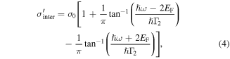
The calculated graphene's relative permittivity as a function of wavelength and Fermi level is shown in figures 1(a) and (b). As shown in figure 1(a), at a given wavelength, ![${\rm{Re}}[\varepsilon (\omega )]$](https://content.cld.iop.org/journals/0957-4484/27/50/505206/revision1/nanoaa49edieqn11.gif) increases first as the Fermi level increases. When the Fermi level is beyond the half of the photon energy, it rapidly decreases as the Fermi level increases, such that the light which interacts with graphene experiences an obvious phase change as the Fermi level increases. On the other hand, figure 1(b) shows that
increases first as the Fermi level increases. When the Fermi level is beyond the half of the photon energy, it rapidly decreases as the Fermi level increases, such that the light which interacts with graphene experiences an obvious phase change as the Fermi level increases. On the other hand, figure 1(b) shows that ![${\rm{Im}}[\varepsilon (\omega )]$](https://content.cld.iop.org/journals/0957-4484/27/50/505206/revision1/nanoaa49edieqn12.gif) is almost unchanged as the Fermi level increases at first. When the Fermi level is beyond the half of the photon energy,
is almost unchanged as the Fermi level increases at first. When the Fermi level is beyond the half of the photon energy, ![${\rm{Im}}[\varepsilon (\omega )]$](https://content.cld.iop.org/journals/0957-4484/27/50/505206/revision1/nanoaa49edieqn13.gif) is reduced sharply and then becomes stable again. The reason for this is that there is no interband transition in the graphene when the Fermi level is beyond the half of the photon energy.
is reduced sharply and then becomes stable again. The reason for this is that there is no interband transition in the graphene when the Fermi level is beyond the half of the photon energy.
Figure 1. Graphene's relative permittivity as a function of wavelength and Fermi level. (a) Real part. (b) Imaginary part.
Download figure:
Standard image High-resolution image2.2. Graphene's relative permittivity in a gaseous environment
Based on these properties of graphene, we design a graphene-based gas sensor with the Fermi level beyond the half of the photon energy in which the graphene induces a negligible optical loss, but a large phase change. Considering the transparent window of silicon-photonic devices (from 1.1 to 8.0 μm for silicon and from 2.0 to 13.0 μm for germanium), we carry out the following calculations within the mid-IR spectral region.
When graphene is exposed to a gas, the carrier concentration of graphene is changed by gas molecules. The relative permittivity of graphene is changed at different gas concentrations. In addition, due to the selectivity of gas adsorption on graphene, the variation in graphene's Fermi level is also related to the gas species. Taking a nitrogen dioxide (NO2) gas as an example, the relation between the carrier density of graphene and the NO2 gas molecule concentration is empirically given by [2]
where C is the carrier concentration of graphene (cm−2) and  is the concentration of the NO2 gas (ppm). Here the details of equation (2) can be found in [2]. It is worthwhile to note that a mixture of NO2 diluted in inert gases (nitrogen and helium) is used in the gas sensing experiment in [2]. Equation (2) should be changed if graphene is used to sense a NO2 gas in the atmosphere due to possible interferences from oxygen and other air pollutants. Moreover, these possible interferences may limit the sensitivity of the proposed photonic gas sensor. The variation in graphene's Fermi level
  can be calculated by

where  is the initial Fermi level before the gas molecules adsorb on the graphene and
  is the final Fermi level after the gas molecules adsorb on the graphene, which is given by [23]

where  is the Fermi velocity, gv = 2 is the valley degeneracy, gs = 2 is the spin degeneracy, and
  is the initial carrier concentration of graphene, which is given by

The variations in the graphene's complex relative permittivity before and after the gas molecules adsorb on the graphene are calculated and shown in figures 2(a) and (b). Here the NO2 gas concentration is chosen as 10 ppm, which corresponds to the variation in the carrier density of 6.03 × 1011 cm−2. At longer wavelengths and lower Fermi levels, the variation in ![${\rm{Re}}[\varepsilon (\omega )]$](https://content.cld.iop.org/journals/0957-4484/27/50/505206/revision1/nanoaa49edieqn20.gif) becomes much larger, which results in a more obvious phase shift of light. Moreover, when graphene is adsorbed by gas molecules, the variation in the carrier concentration in the graphene sensor is limited compared to that in the electro-optic modulator [21]. Due to the linear dispersion of graphene's energy band diagram, the carrier density is proportional to the Fermi level. Therefore, for a given carrier concentration change, variations in graphene's Fermi level and permittivity are small at high Fermi levels. This shows that the Fermi level of graphene cannot be too large if we want to achieve a sensitive gas sensor. On the other hand, the variation in
becomes much larger, which results in a more obvious phase shift of light. Moreover, when graphene is adsorbed by gas molecules, the variation in the carrier concentration in the graphene sensor is limited compared to that in the electro-optic modulator [21]. Due to the linear dispersion of graphene's energy band diagram, the carrier density is proportional to the Fermi level. Therefore, for a given carrier concentration change, variations in graphene's Fermi level and permittivity are small at high Fermi levels. This shows that the Fermi level of graphene cannot be too large if we want to achieve a sensitive gas sensor. On the other hand, the variation in ![${\rm{Im}}[\varepsilon (\omega )]$](https://content.cld.iop.org/journals/0957-4484/27/50/505206/revision1/nanoaa49edieqn21.gif) should be small, such that fluctuations in the optical loss in the waveguide are negligible for photonic devices. As a result, photonic gas sensors are preferred to work in the long wavelength and low Fermi level regions. As the propagating light is greatly absorbed by silicon if the wavelength is beyond 8 μm, the wavelength of 8.0 μm and the initial Fermi level of 0.1 eV are chosen for GoS devices in our simulation below. The germanium waveguide can be used at an extended wavelength of 13.0 μm [24], such that the sensitivity of the photonic gas sensor can be further improved.
should be small, such that fluctuations in the optical loss in the waveguide are negligible for photonic devices. As a result, photonic gas sensors are preferred to work in the long wavelength and low Fermi level regions. As the propagating light is greatly absorbed by silicon if the wavelength is beyond 8 μm, the wavelength of 8.0 μm and the initial Fermi level of 0.1 eV are chosen for GoS devices in our simulation below. The germanium waveguide can be used at an extended wavelength of 13.0 μm [24], such that the sensitivity of the photonic gas sensor can be further improved.

Figure 2. Variations in graphene's relative permittivity as a function of wavelength and Fermi level when graphene is exposed to NO2 gas at a concentration of 10 ppm. (a) Real part. (b) Imaginary part.
Download figure:
Standard image High-resolution image3. GoS-SMSWs
The proposed GoS-SMSW is schematically shown in figure 3(a). A mid-IR silicon waveguide is designed based on a commercial silicon-on-insulator wafer with a 500 nm thick top silicon layer and a 3 μm thick buried oxide (BOX). The waveguide structure can be patterned by using electron beam lithography (EBL) and transferred onto the top silicon layer by using the deep reactive-ion etching process. Since the BOX has an extremely strong absorption to the propagating light when the wavelength is beyond 2.5 μm, the BOX below the top silicon device can be removed by using the chemical wet etching process in a hydrogen fluoride solution. As shown in figure 3(b), the silicon waveguide can be supported by two-side cantilevers. After fabricating the silicon chip, graphene can be integrated onto the waveguide by using the wet transfer process. Finally, the graphene layer can be patterned by using the EBL and oxygen plasma etching. All the fabrication steps are CMOS compatible. Details of fabricating the suspended membrane devices can be found in previous reports [16–19, 25]. Similar structures can be fabricated based on a germanium-on-insulator wafer [24].
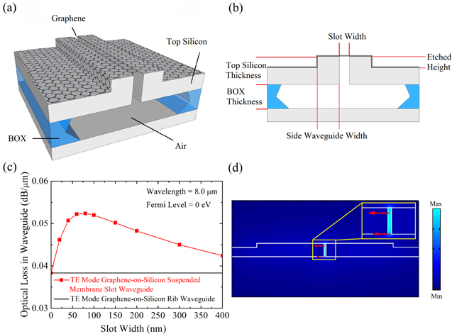
Figure 3. Design of the GoS-SMSW. (a) Three-dimensional schematic of the waveguide. (b) Schematic of the waveguide cross section. (c) Simulated optical absorption of the waveguide and its comparison with that of a TE mode GoS rib waveguide. (d) Eclectic filed distribution of the GoS-SMSW. The insert shows an enlarged view of the slot region. The arrows indicate the direction of the electric field.
Download figure:
Standard image High-resolution imageFor developing sensitive photonic gas sensors, it is important to consider the interaction of propagating light in the waveguide to the top graphene layer. Here the light can be used to probe variations in graphene's relative permittivity caused by gas molecules which adsorb on the sensor. As the variations are small at a low gas concentration, it is crucial to increase the interaction of the light with the top graphene layer. By applying the calculated relative permittivity of graphene into a commercial software tool (COMSOL Multiphysics), we simulate optical losses in different GoS waveguides. Two types of suspended membrane waveguide structures, namely, rib waveguides and slot waveguides, are studied with different parameters at a wavelength of 8.0 μm under the Fermi level of 0 eV. Simulation results are shown in figure 3(c). For the GoS rib waveguide, we choose the waveguide width as 5 μm and the etched height as 150 nm which ensures the condition for the propagating light in the fundamental transverse electric (TE) mode. According to the simulation, the optical loss is 0.038 dB μm−1 for the TE mode GoS rib waveguide (indicated by the black line in the figure). For the TE mode GoS-SMSW, we choose the side waveguide as 2.5 μm and the etched height as 150 nm. The slot width varies from 0 to 400 nm. The simulation results show that the GoS-SMSW has a larger optical absorption than that of the GoS rib waveguide, which shows a stronger light interaction with the top graphene layer. This is because the electrical field in the slot region has discontinuity at the high refractive index (RI) contrast interface. This discontinuity can be used to strongly confine light in the slot region [26], as shown in figure 3(d). Another possible reason for the enhancement is the loose mode confinement for the slot waveguide (with an effective RI of 1.784 279) compared to the rib waveguide (with an effective RI of 1.925 608). On the other hand, a wider slot size provides a larger interaction area between the top graphene layer and the propagating light, but the light intensity enhancement is reduced. Therefore, there is an optimum width which gives the maximum interaction. Figure 3(c) shows that the optimized slot width is 80 nm which provides the maximum absorption of 0.052 dB μm−1 (indicated by the red curve). This feature size can be achieved in the CMOS fabrication process.
4. Waveguide-integrated photonic gas sensors
Based on the GoS-SMSW, we propose and simulate a photonic gas sensor based on the Bragg grating structure shown in figure 4(a). The Bragg grating can be designed by using the coupled-mode theory [27]. The power reflection spectra of the Bragg grating can be estimated using the equation [28]

where  is the length of the Bragg grating and κ and
  are the 'ac' coupling and 'dc' self-coupling coefficients of the Bragg grating, which are given by


where  is the optical wavelength in vacuum,
  is the average effective RI of the Bragg grating,
  is the grating period, and
  is the 'dc' index change spatially averaged over the grating period. We choose L = 4 mm and Λ = 2241 nm to calculate the reflection spectra of the Bragg grating at the center wavelength of 8 μm. Our COMSOL simulation shows that the effective RIs of the GoS-SMSW are found to be 1.782 762, 1.782 21, and 1.778 506 at NO2 gas concentrations of 0 ppm, 1 ppm, and 10 ppm, respectively. Without the graphene covering the waveguide, the effective RI of the silicon slot waveguide is simulated as 1.784 279. As shown in figure 4(b), the central reflection bandwidth increases as the NO2 gas concentration increases. This is because the effective RI of the graphene-covered slot waveguide decreases when gas molecules adsorb on the graphene. Our calculations show that at the center wavelength of 8 μm and the Fermi level of 0.1 eV, variations in the 3 dB bandwidth of the zeroth-order power reflection are 1.2 and 9.6 nm at NO2 gas concentrations of 1 ppm and 10 ppm, respectively, which correspond to the normalized bandwidth
  of 1.5 × 10⁻⁴ and 1.2 × 10⁻³, respectively.

Figure 4. Design of the GoS-SMSW Bragg grating gas sensor in comparison with the graphene-covered microfiber Bragg grating gas sensor. (a) Schematic of the GoS-SMSW Bragg grating gas sensor. (b) Reflection spectra of the GoS-SMSW Bragg grating gas sensor for sensing the NO2 gas. The black, red, and blue curves represent the Bragg grating reflection spectra at 0ppm, 1ppm, and 10 ppm NO2 gas concentrations, respectively. (c) Schematic of the graphene-covered microfiber Bragg grating gas sensor. (d) Reflection spectra of the graphene-covered microfiber Bragg grating gas sensor for sensing the NO2 gas. The red and black curves represent the Bragg grating reflection spectra at 0 ppm and 20 ppm NO2 gas concentrations, respectively.
Download figure:
Standard image High-resolution imageFor comparison, a similar calculation is carried out to predict the performance of the graphene-covered microfiber Bragg grating sensor, as schematically illustrated in figure 4(c). The grating length and period are chosen as 2 mm and 596 nm, respectively. The diameter of the microfiber is chosen as 10 μm which is a common size used in previous experiments [13, 14, 29]. Due to the limited transparent window of silicon dioxide, the microfiber can only work from the visible to near-IR spectral region. Here we choose the wavelength as 1.55 μm and the initial Fermi level as 0.1 eV. Our COMSOL simulation results indicate that the effective RI of the microfiber is 1.298 889. With the graphene covering the fiber, the effective RI is simulated as 1.299 098 and 1.299 111 at NO2 gas concentrations of 0 ppm and 20 ppm, respectively. Similar to the GoS-SMSW Bragg grating gas sensor, the power reflection bandwidth increases with the increase of the NO2 gas concentration, as shown in figure 4(d). However, the variation in the 3 dB bandwidth of the zeroth-order power reflection is only 0.08 nm at the NO2 gas concentration of 20 ppm. The normalized bandwidth  is 0.6 × 10⁻⁴ which is comparable with that of the GoS-SMSW Bragg grating gas sensor at the NO2 gas concentration of 1 ppm. Therefore, the sensitivity of the proposed gas sensor is approximately a factor of 20 higher than that of the graphene-covered microfiber gas sensor. The reason for the lower sensitivity of the graphene-covered microfiber is that the shorter wavelength of the propagating light corresponds to a smaller variation in graphene's relative permittivity as shown in figure 2(b). In addition, the microfiber structure provides a better confinement to the propagating light such that the interaction of the light to graphene is weak in this sensor type.
Comparing figures 4(b) and (d), there is an obvious difference in gas sensing sensitivity between the two types of waveguide. The calculated 3 dB bandwidth of the proposed GoS and GoG-SMSW Bragg gratings as a function of the NO2 gas concentration is shown in figure 5. By integrating an on-chip spectrometer with a channel spacing of 10 GHz [15] into the device, the sensitivity of the NO2 gas sensor based on the GoS slot waveguide Bragg grating can reach a level of ∼3 ppm. The sensitivity can be further improved by using the GoG slot waveguide since it can be operated at a longer wavelength. Our calculations show that with the slot width of 80 nm, the maximum sensitivity of the GoG-SMSW Bragg grating sensor can reach a level of ∼1 ppm at the wavelength of 13.0 μm and the Fermi level of 0.1 eV. For NO2 gas sensing, the sensitivity of both types of photonic gas sensors can reach the Permissible Exposure Limit given by the Occupational Safety & Health Administration in the United States (5 ppm) [30].

Figure 5. Comparison in the 3 dB power reflection bandwidth between the GoS (black line) and GoG (red line) SMSW Bragg gratings as a function of the NO2 gas concentration.
Download figure:
Standard image High-resolution image
Finally, we compare three types of graphene-based photonic gas sensing techniques: (i) microfiber sensors, (ii) plasmonic sensors, (iii) waveguide-integrated sensors. As shown in table 1, the proposed waveguide-integrated Bragg grating gas sensor has a comparable sensitivity with that of the theoretically proposed plasmonic gas sensor. It is slightly lower than the sensitivity of the graphene-covered optical waveguide which can reach 0.2 ppm and 0.5 ppm for ammonia and xylene gas sensing, respectively. It is worthwhile to note that the high-resolution on-chip spectrometer can be useful for further improving the sensitivity of the proposed waveguide-integrated gas sensor. In addition, as the proposed photonic gas sensor works within the mid-IR spectral region, it has chemical specificity due to the strong and distinctive fundamental vibrational and rotational transitions of gas molecules in the spectral region. With the rapid development of chip-integrated mid-IR lasers, such as quantum cascade lasers, it is promising to realize the monolithic integration of the graphene gas sensor with other photonic and electronic devices. The chip-integrated graphene gas sensor may boost the future development of portable sensing devices and various applications.
Table 1. Comparison of different configurations of graphene-based photonic gas sensors.
| Microfiber sensors | Plasmonic sensors | Waveguide-integrated sensors | |
|---|---|---|---|
| Spectral region | Visible to near-IR | Mid-IR to low-THz | Near-IR to mid-IR |
| Sensitivity | <1 ppm [12] | 1 ppm [14] | <1 ppm |
| Advantages | Convenient for building a sensor network | Compact | Compact, low cost, monolithically integratable with photonic and electronic devices |
| Potential applications | Distributed sensing networks | Compact sensors | Gas sensing devices installed in portable devices |
5. Conclusions
In summary, we present the design of mid-IR slot waveguide-integrated graphene Bragg gratings for sensitive photonic gas sensing. The charge transfer from adsorbed gas molecules to the graphene induces variations in graphene's conductivity and the phase of the interacting light. The mid-IR slot waveguide structure is designed to enhance the interaction between the top graphene layer and the propagating light in the waveguide. The waveguide Bragg grating acts as an interference structure to transform the phase shift of the propagating light into the change in the output power spectrum. The sensitivity of the proposed waveguide-integrated gas sensor can reach ∼1 ppm, which is approximately a factor of 20 higher than that of the graphene-covered microfiber gas sensor and comparable with that of the plasmonic gas sensor. This study paves a way for chip-integrated sensitive gas sensors.
Acknowledgments
The work was partly supported by Konica Minolta Imaging Science Encouragement Award, MEXT APSA, and Burroughs Wellcome Foundation. We thank Jeffrey Harmon for helping with revisions to the manuscript.