
Abstract
Nanowire based solar cells have attracted great attention due to their potential for high efficiency and low device cost. Photovoltaic devices based on InP nanowires now have characteristics comparable to InP bulk solar cells. A detailed and direct correlation of the influence of growth conditions on performance is necessary to improve efficiency further. We explored the effects of the growth temperature, and of the addition of HCl during growth, on the efficiency of nanowire array based solar cell devices. By increasing HCl, the saturation dark current was reduced, and thereby the nanowire solar cell efficiency was enhanced from less than 1% to 7.6% under AM 1.5 illumination at 1 sun. At the same time, we observed that the solar cell efficiency decreased by increasing the tri-methyl-indium content, strongly suggesting that these effects are carbon related.
Export citation and abstract BibTeX RIS
1. Introduction
Energy generation via photovoltaic devices is a prominent research topic as solar power is a renewable, clean and abundant source [1]. Its development, though, has been curbed by the conflicting requirements of high efficiency and low cost [2, 3]. Nanowires have strong potential to disentangle the current impasse, with an efficiency up to 15.3% demonstrated recently in the literature [4, 5], due to several advantages. The most well known is lower material consumption, compared to bulk [6, 7], which correlates to a high absorption-to-volume ratio [8, 9] and the possibility of re-using the substrate. Moreover, the morphology of nanowires enables straightforward realization of flexible solar cells [10]. At the same time, the reduced surface coverage implies that elastic relaxation of lattice-mismatch induced strain is possible [11], allowing a broader material choice for multi-junction solar cells, and thus granting the opportunity of realizing higher efficiency photovoltaic devices [1]. Additionally, for solar cell applications, the nanowire geometry is inherently superior to bulk due to its enhanced light out-coupling and reduced non-radiative recombination rate [12, 41]. Previous studies have shown that nanowires with 180 nm diameter, 1.5 micron length and a 500 nm wire-to-wire spacing, feature optimum solar light absorption for III–V nanowire arrays such as InP and GaAs [4, 5]. In order to realize wires with such large diameters, and at the same time good electrical and optical properties, the growth parameters have to be optimized. Two key growth parameters are the growth temperature and the HCl molar fraction. Higher temperatures have been shown to diminish the presence of impurities [13], and lower the density of crystalline defects of the nanowires [14]; both impurities and crystalline defects have a detrimental effect on device efficiency [15, 16]. HCl, added during growth, is used for suppressing side facet growth, which yields a shell with a lower electronic quality than material grown directly via the catalyst particle [17, 18]. In this article, we study the effect of these two factors on the efficiency of photovoltaic devices based on nanowire arrays with ideal morphology for light absorption. In addition, a scheme for achieving high vertical yield and good morphology of the nanowire arrays is discussed.
2. Experimental details
Nanowires were grown in a low-pressure Aixtron Closed Coupled Showerhead (CCS) metalorganic vapor phase epitaxy (MOVPE) machine. Hydrogen (H2) was used as a carrier gas for the precursors, with a total gas flow of 6 l min−1 at a pressure of 50 mbar. Axial p–i–n junctions were obtained by doping nanowires in situ with diethyl-zinc (DEZn, as p-dopant) and hydrogen sulfide (H2S, as n-dopant). Nanowires are grown on (111)B InP substrates using the vapor–liquid–solid method, in which Au droplets act as catalysts. To realize a nanowire array with diameter ≈180 nm, optimum for light absorption, Au disks with a thickness of 40 nm and a diameter of 240 nm were patterned with a square symmetry and a pitch of 513 nm, by nanoimprint lithography on a 2 in wafer [19, 20]. Tri-methyl-indium (TMI) and phosphine (PH3) were used as group III and V precursors. Before nanowire growth, an annealing step at 510 °C under PH3 atmosphere was performed to remove organic residues from the nanoimprint process. HCl was used in situ to suppress tapering of the nanowires [17], with different molar fractions. The HCl molar fraction was kept constant during growth for both p- and n- doping segments. The ∼200 nm nanowire diameter was defined by the amount of Au catalyst, which was kept constant for all of our samples. The growth times of the p- and n-doped segments was varied to control the nanowire length within a range 1.3–1.5 μm, and position the intrinsic region halfway along the nanowire length. We chose this doping configuration, even though it is not optimal [21], to reduce the number of variables affecting the performance of the solar cells.
To fabricate nanowire array solar cell devices we followed, with minimal deviation, a procedure described earlier in the literature [22]. After growth, the nanowires were etched using a Piranha solution for 50 s, to remove surface defects and shunting paths that cannot be removed by in situ HCl, as previously demonstrated [22]. The result was a nanowire array with a final nanowire diameter of 170 nm, which is ideal for solar light absorption. A 50 nm layer of silicon oxide (SiO2) was then deposited by plasma-enhanced chemical vapor deposition. To planarize the device and to isolate the top from the back contact, benzocyclobutene (BCB) was used to fill in the spaces between the nanowires, and was cured in a vacuum oven. The BCB was subsequently etched back by reactive ion etching in order to expose the tips of the nanowires (the open segment was 200–300 nm long). Au particles on top of the nanowires were removed by wet etching in KI/I2 solution. After this step, the SiO2 on the top of the nanowires was removed by a short dip in buffered hydrofluoric acid (BHF 7:1) and 300 nm of indium tin oxide (ITO) was sputtered as a transparent conductive oxide. A final optical lithography step was used to define 500 × 500 μm ITO pads, which act eventually as the cell area for solar cell devices. As back contact, a p-doped InGaAs layer was grown by MOVPE on the backside of the complete 2 in InP wafer, on the opposite side of nanowire growth. The step was performed prior to nanoimprint lithography, which was then done on the polished front-side where the nanowires were then grown [22]. Ti/Pt/Au multi-layers were then deposited as a contact layer, to obtain ohmic contact to the substrate. The performance of the nanowire array solar cell devices was subsequently evaluated by current–voltage measurements in a two terminal electrical setup. A xenon lamp simulating the AM 1.5 solar spectrum was used as a light source. The lamp was calibrated using a GaAs reference photovoltaic cell supplied by ReRa B.V.
The nanowire arrays were imaged on cleaved samples by using a Zeiss Sigma field emission scanning electron microscope (SEM) operating at 3 kV. Imaging was performed at either 30° or 90° tilt compared to the normal to the surface.
Atom probe tomography (APT) was performed using a Cameca LEAP 4000X HR. The system was equipped with a laser generating picosecond pulses at a wavelength of 355 nm. For the analysis, samples were cooled down to a temperature of 20 K. The experimental data were collected at a laser pulse rate of 65–100 kHz at laser powers between 0.6 and 1 pJ. APT data were reconstructed using IVAS 3.6.8 and visualized using AtomBlend in Blender 2.7.6. Depth-profiles were extracted from the APT data by slicing the reconstructed 3D volume perpendicular to the growth axis and determining the fraction of atoms of each element detected in the resulting sub-volumes from a background-corrected local mass spectrum [23]. Errors were estimated for each element as the sum of the expected statistical counting errors [24] and the fluctuations in the background signal next to the respective elemental peaks.
3. Results
Before proceeding to the fabrication of solar cell devices, optimization of the nanowire growth is needed to obtain an optimum nanowire array geometry for sufficient light absorption and a uniform nanowire distribution, which grants stable electrical behavior of the cells. The nanowire diameter and pitch were determined using a nanoimprint mask and Au layer thickness. We used a distance of 513 nm between the nanowire centers. In order to obtain nanowires with diameters of the order of 180–200 nm, we deposited a relatively thick Au disk (40 nm) with a diameter of 241 nm. If growth proceeds without any further steps, the vertical yield and the uniformity, in the case of these relatively thick nanowires, are both relatively low. In fact, the Au droplets, which were all in the intended position before growth, can split, move on the substrate and/or merge with other Au particles. As a result, nanowires were missing from the pattern or had a diameter noticeably divergent from what was intended (see figures 1(a) and (c)). In order to reduce this effect, we added a step, performed before the annealing phase at 510 °C, in which the sample was pre-heated at 370 °C for 5 min in PH3/H2 atmosphere (PH3 was switched on at a temperature of 300 °C, to prevent phosphorous evaporation from the InP substrate). With this step, the Au catalysts were fixed to their position, preventing them from moving across the substrate surface (figures 1(b) and (d)). The vertical yield of nanowires, averaged over arrays of 10 × 10 nanowires, increases from 45 ± 17% to over 99%, while the diameter changed from 195 ± 43 to 201 ± 6 nm (relative standard deviation reduced from 22% to 3%). The Au catalysts reacted with the InP substrate below them [25–27, 42] during this pre-growth step, restraining them from changing location and guaranteeing a high vertical yield, as is evident by comparing figures 1(c) with (d).
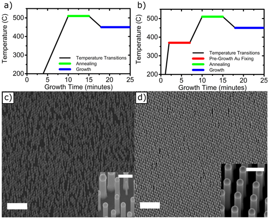
Figure 1. Pre-growth Au fixing. Scheme of the temperature sequence during nanowire growth, (a) without and (b) with pre-growth fixing of the Au particle to its position (PH3 is always switched on in these schemes). SEM image of sample after 10 min growth, (c) without and (d) with pre-growth Au fixing. Scale bars are 5 μm. The insets show corresponding higher magnification SEM images, with 1 μm scale bar.
Download figure:
Standard image High-resolution imageOnce the morphology of the nanowire array was adequate, the first parameter we investigated to optimize the performance of nanowire solar cells was the growth temperature. The growth temperature has also been shown to influence the crystalline structure of undoped InP nanowires, and to affect the presence of impurities, in bulk InP [13, 28]. We varied the growth temperature from 450 °C up to 510 °C. At 510 °C, as has been previously reported in several cases [25, 29, 30], growth became very unstable and it was difficult to obtain vertical nanowires with good morphology without considerably altering the growth conditions (see online supplementary data). Therefore, we could not use these arrays for further processing. In the range 450–490 °C, the nanowires were uniform under analogous growth conditions. We processed these nanowire samples to fabricate nanowire solar cells, and the results are shown in figure 2(a). We clearly see an improvement in the solar cell performance with the increase of growth temperature. Additionally, we observed a small decrease in the dark current. Table 1 lists the characteristic parameters (open circuit voltage, short circuit current, fill factor, and efficiency, respectively Voc, Isc, FF, and η) for the different growth temperatures. An overall enhancement with increasing temperature is evident. It has been shown previously that increasing the growth temperature of undoped nanowires can: (1) lower the density of stacking faults and induce a homogeneous crystalline structure [14]; and (2) decrease the incorporation of non-radiative recombination centers [13]. We will further focus on the details of these non-radiative centers in the discussion section. Both these effects would be expected to have a favorable effect on the optical properties and on the photovoltaic performance. We have not seen an effect of temperature on the crystalline structure, from transmission electron microscopy (TEM) analyses. The nature and concentration of the intentional dopants has, in fact, the most dominant effect on the crystalline structure. As a result, the zincblende structure, with several twins (tens/μm), is predominant in the p-doped segment, while the n-doped segment exhibits the wurtzite structure, with a high stacking fault density (hundreds/μm), as has also been demonstrated previously (figure 2(b)) [22, 31]. Post-growth rapid thermal annealing was also performed, but no improvement of performance was observed.
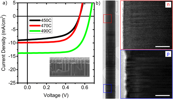
Figure 2. Effect of the growth temperature on the nanowire solar cell performance. (a) I–V curves of solar cells based on nanowire arrays grown at temperatures of 450 °C, 470 °C, and 490 °C. The HCl molar fraction is 1.3 × 10⁻⁶. The inset shows an SEM image of a device after processing. Scale bar is 1 μm. (b) TEM image showing an overview of a p-n-doped 〈111〉 InP nanowire. Scale bar is 250 nm. The two insets show HRTEM images of zoomed-in sections of p- and n-doped segments. Scale bars are 50 nm. Growth temperature is 490 °C.
Download figure:
Standard image High-resolution imageTable 1. Solar cell performance parameters (Jsc, Voc, FF and efficiency η) as a function of growth temperature. The HCl molar fraction is 1.3 × 10⁻⁶.
| Growth temperature | Short circuit current Jsc (mA cm−2) | Open circuit voltage Voc (V) | Fill factor (FF) | Efficiency (η) |
|---|---|---|---|---|
| 450 °C | 8.8 ± 0.4 | 0.55 ± 0.10 | 0.6 ± 0.1 | 2.8 ± 0.6 |
| 470 °C | 9.8 ± 0.4 | 0.55 ± 0.10 | 0.65 ± 0.05 | 3.5 ± 0.7 |
| 490 °C | 13.7 ± 0.5 | 0.66 ± 0.10 | 0.70 ± 0.05 | 6.3 ± 1.1 |
The second parameter we studied is the HCl molar fraction, χHCl. HCl is used to prevent lateral growth on the side facets of the nanowires. It is an excellent means employed to avoid tapering without altering other growth conditions [17]. The effect of HCl on the solar cell performance, though, is largely unexplored. We varied χHCl by a factor of three (from 5 × 10⁻⁷ to 1.6 × 10⁻⁶) without changing any other parameters, apart from the growth time, modified to take into account the reduced growth rate, so that the total length of the nanowire is kept constant [17]. Using an χHCl lower than 5 × 10⁻⁷ results in nanowire tapering, as has been proven before in the literature [17, 22], while a molar fraction higher than 1.6 × 10⁻⁶ yields a growth rate several times lower, and often leads to a kinked nanowire morphology (see online supplementary data). We observed that varying the χHCl within this range does not affect either the morphology or the crystalline structure of the nanowires. In particular, we did not observe a change in the density of the crystalline defects such as twins and stacking faults. The optoelectronic properties of the nanowire devices, instead, were dramatically affected by changing the HCl molar fraction.
We first focus on the dark saturation current of nanowire solar cells (figure 3(a)). The dark current is related to the density of non-radiative recombination centers in the bulk of the wires, such as unintentional impurities, crystalline and point defects. We observed a sharp decrease of three orders of magnitude in the dark current by increasing χHCl by a factor of three. The nanowire solar cells were subsequently studied under AM 1.5 illumination at 1-sun intensity (figures 3(b)–(c)). All performance parameters (Voc, Jsc, and FF) clearly improved by increasing χHCl. The increased standard deviation in Jsc and FF is explained by the presence of kinked wires, which was observed for χHCl larger than 1.2 × 10⁻⁶. Even a small number of kinked wires significantly decreases the probability of contacting all the nanowires with a thin ITO top contact layer, introducing leakage current and shunting paths, as p-doped regions are short-circuited. We now focus on the relation between the increase in Voc and the decrease in the dark current  In fact, the open circuit potential can be expressed as:
where n is the ideality factor, k is the Boltzmann constant, Tc is the temperature of the solar cell, and q is the elemental charge of electrons. According to this equation, a decrease of three orders of magnitude of J0 should correspond to a linear increase in Voc by approximately a factor of three. This is consistent with the observed enhancement (see figure 3(d)). The highest efficiency achieved was 7.6%, with a Voc of 0.61 V, Jsc of 18.2 mA cm−2 and FF of 0.68, at an HCl molar fraction of of 1.46 × 10⁻⁶. Use of a higher χHCl is possible, but the growth rate reduces dramatically, making such growth impractical. Furthermore, a very high χHCl favors nanowire kinking and a general degradation of morphology, which negatively affects the solar cell performance. This dataset demonstrates that Voc is directly correlated to the saturation dark current, as expected, and that HCl can improve substantially the performance.

Figure 3. Effect of HCl on solar cell performance. Log J–V characteristics in the dark (a) and linear J–V at 1-sun illumination (b) for nanowire solar cells with different HCl molar fraction. (c) Measured Voc, FF and Jsc for nanowire solar cells with different HCl molar fraction. (d) Measured Voc as function of the ratio of Jsc and J0. All growth was performed at a temperature of 490 °C.
Download figure:
Standard image High-resolution imageA possible reason for the improvement of the characteristics of the nanowire solar cells is the reduction of unintentional impurities, which act as recombination centers. A common impurity in MOCVD growth is carbon, introduced by the metalorganic precursors. To study a possible adverse effect of carbon on the cell performance, we grew nanowires at a temperature of 490 °C with a constant χHCl (1.2 × 10⁻⁶) and increased the TMI molar fraction, effectively augmenting the amount of carbon present during growth. There was no effect on the morphology of the nanowires, which were not tapered and have similar growth rate; also, the crystalline structure is unchanged. The performance of the solar cells obtained was instead clearly degrading with increasing TMI molar fraction (figures 4(a)–(b)). Voc, Jsc and FF all declined when the TMI molar fraction was increased in the reaction chamber, and an increase in the dark current was observed at the highest TMI molar fraction. These measurements indicate that the amount of TMI, or more accurately the ratio between TMI and HCl, is critical for solar cell performance.

Figure 4. Effect of TMI on the solar cell performance. (a) J–V characteristics at 1 sun illumination for nanowire solar cells with different TMI molar fractions. (b) Measured Voc, FF and Jsc for nanowire solar cells with different TMI molar fractions. All samples were grown at 490 °C with a HCl molar fraction of 1.2 × 10⁻⁶.
Download figure:
Standard image High-resolution imageSince the growth rate changes with varying χHCl and with temperature, the intentional doping concentration can be slightly different between samples. This change is not expected to drastically affect the performance, but it introduces an additional variable that is difficult to control. A thorough doping study is out of the scope of this article, but to exclude a significant effect of the growth conditions on the dopant concentration, we performed atom probe tomography (APT) measurements on single InP nanowires extracted from the solar cells. We observed no substantial differences in the concentration of dopants when comparing nanowires from samples grown at the extremes of our experimental range. One sample was grown at low HCl and high TMI molar fraction (5 × 10⁻⁷ and 1.16 × 10⁻⁵, respectively), a second at high HCl and lower TMI molar fraction (1.2 × 10⁻⁶ and 8.9 × 10⁻⁵, respectively), with all other growth parameters identical. The doping concentrations measured were in the range of a few ppm, which resulted in 1017 cm−3. A typical 3D APT reconstruction of a nanowire extracted from the first sample is shown in figure 5.
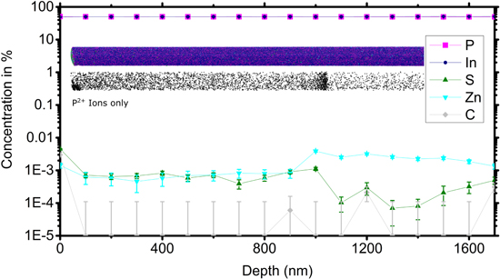
Figure 5. APT measurements of a single InP nanowire taken from a solar cell, grown with HCl and TMI molar fractions of 5 × 10⁻⁷ and 1.16 × 10⁻⁵, respectively. The axial concentration profile extracted from the APT analysis locates the p-n-doped InP nanowire. No evident carbon signal can be detected. The error estimate for the carbon detection indicates a sensitivity to carbon of 1 × 1017 cm−3. Insets: position of the atoms in the 3D APT reconstruction (top, only 5% of In and P shown for clarity) and positions of doubly charge P ions (bottom). As the abrupt change in the presence of doubly charged P ions is caused by a change in the material properties, it substantiates the presence of the p-n junction at this position.
Download figure:
Standard image High-resolution image
The figure shows the concentration profiles of In, P, S, Zn, and C extracted from the APT analysis overlapped with two representations of the reconstructed 3D volume—one showing the reconstructed positions of all ions and one highlighting the position of the doubly charged phosphorus ions (P2+). The concentration profiles suggest that the p-n junction is at a depth of 1000–1100 nm in this wire. At the same position, an abrupt change in the presence of doubly charged phosphorus ions is observed.
The charge state of the ions in APT is known to be related to the electric field on the surface of the analyzed sample [32] and an abrupt change in the electric field necessary to remove ions from the sample surface is likely to be related to a change in the material properties [33]. The abrupt change in the number of P2+ ions is thus another indication for the presence of the p-n junction at this depth.
4. Discussion
We now discuss different possibilities for the origin of the observed effects: the improvement of nanowire solar cell performance with increased temperature and HCl molar fraction, and the degrading effect of an increase in TMI molar fraction. Several explanations are possible: surface states and shunting paths, planar crystalline defects, point defects, and unintentional impurities.
Surface states and shunting paths can be ruled out, as we always removed a layer of about 25 nm from the nanowire sidewalls directly after growth, which was demonstrated in a previous work as being effective in removing possible as-grown shunting paths and surface impurities [22]. Since the surface is etched, it is the same for all types of wire in our study, excluding an effect from it.
The effect of changes in the density of planar crystalline defects (like stacking faults and twins) can also be excluded, as we have seen no influence of growth conditions on the crystalline structure of nanowires, evidenced by the TEM study. The improved solar cell performance at higher growth temperature should thus be explained by a reduced number of non-radiative recombination centers, such as point defects, like vacancies and anti-sites, and/or unintentional impurities.
A possible explanation is related to the incorporation of unintentional impurities [17, 28]. As we saw no significant changes in the concentration of the Zn and S dopants, measured by APT in samples with dramatically different growth conditions, we can also exclude their effect. The most likely unintentional impurity in MOVPE growth is then carbon, originating from the metalorganic precursors used, as In(CH3)3 (TMI) and (C2H5)2Zn (DEZn) are used as precursors for In and Zn, respectively. Carbon acts as a donor (n-type dopant) in InP, so that it can partially compensate for the intentional Zn-doping in the p-doped region, and perturb S-doping in the n-doped region [34, 35]. Our strongest argument in favor of carbon is the fact that the solar cell performance heavily degrades with increasing TMI flux. Both the growth temperature and HCl are also expected to affect carbon; temperature has been shown before to be crucial to reduce carbon incorporation, both in bulk layers and nanowires [13, 28], while it is known that HCl can react with TMI in the gas phase to form InCl3, removing methyl groups from In, which results in less incorporation of C in the InP wires [36].
As shown in figure 5, where the sensitivity of APT to carbon is in the range of 1 × 1017 cm−3, no clear carbon signal is detected. Nevertheless, even a carbon concentration as low as 1016 cm−3 can influence the performance of the devices [37]. We thus conclude that although carbon is a clear suspect for decreasing the solar cell performance, we cannot provide conclusive evidence. As an alternative explanation, a decrease in the density of point defects might also explain the improved solar cell efficiency, as point defect formation is known to be influenced by growth conditions, even though direct measurement of their presence in nanowires is not straightforward [38, 39]. Most likely, thus, the enhanced performance can be explained by a combination of effects related to the reduction of carbon impurities and/or point defects.
The results above give a deeper insight into the influence of basic growth conditions on the performance of nanowire solar cells. However, the efficiency demonstrated in this work is lower than previously reported efficiencies [4, 22]. As the APT analysis indicates diffusion of Zn into the nominally S doped top layer, elimination of the intermixing of p- and n-dopants in the nominally n-doped top region of the wires can be expected to further improve the performance of our devices. Furthermore, we note that the dopant profile design used is not ideal [4, 21], and we expect that the performance of the devices can be strongly enhanced by its optimization [40].
5. Conclusion
We have studied the effect of important growth parameters on the performance of solar cells based on InP nanowire arrays. We showed that the growth temperature, the HCl molar fraction, and the TMI molar fraction, have a huge influence on the efficiency of solar cells. Carbon incorporation or point defects are suggested to be the key factor in solar cell performance, and their reduction appears to be a straightforward path towards improved efficiency, together with optimization of the doping profile. We have shown solar cell efficiencies as high as 7.6%. Knowledge of the factors that limit the current performance of nanowire solar cells will enable realization of high efficiency devices [43].
Acknowledgments
This research is supported by the Dutch Technology Foundation STW (Project 11826), which is part of the Netherlands Organisation for Scientific Research (NWO), and which is partly funded by the Ministry of Economic Affairs. We acknowledge the long-term energy and innovation program EOS-LT, which is funded by Agentschap NL, as well as the Cobra research school funded by NWO. We would like to acknowledge Solliance for funding the TEM facility and the Investment Subsidy NWO Large for funding the Atom Probe facility. We would like to acknowledge Rene Van Veldhoven for the exceptional work and care for the MOVPE systems, and the technical support from the NanoLab@TU/e cleanroom. The authors thank Vavara Efremova, Anna Ceguerra, Simon Ringer and Peter Felfer from the University of Sydney for the development of the AtomBlend plug-in.