

Abstract
Material used in flexible devices may experience anisotropic strain with identical magnitude, outputting coherent signals that tend to have a serious impact on device reliability. In this work, the surface topography of the nanoparticles (NPs) is proposed to be a parameter to control the performance of strain gauge based on tunneling behavior. In contrast to anisotropic tunneling in a monolayer of spherical NPs, electron tunneling in a monolayer of urchin-like NPs actually exhibits a nearly isotropic response to strain with different loading orientations. Isotropic tunneling of the urchin-like NPs is caused by the interlocked pikes of these urchin-like NPs in a random manner during external mechanical stimulus. Topography-dependent isotropic tunneling in two dimensions reported here opens a new opportunity to create highly reliable electronics with superior performance.
Export citation and abstract BibTeX RIS
Introduction
As a quantum mechanical phenomenon, where an electron flows through a potential barrier that it could not surmount classically, electron tunneling plays an essential role in a wealth of physical phenomena and functional devices, such as the nuclear fusion occurring in the Sun [1], the tunneling diode [2, 3], quantum computing and communication [4], the scanning tunneling microscope [5], plasmonic substrates [6–9], mechanical sensors [10–13] and flexible electronics [14–16]. Ultrathin dielectric layer sandwiched by two conductors is an ideal configuration to mathematically model 1D tunneling [17, 18], and this model can be extended to describe hybrids with 3D stacking by introducing a percolation term that considers the statistical distribution of conductive channels [19]. In this case, macroscopic conductivity G is given as [19]:
where (i) G0 is a constant; (ii) d is the crevice size and ξ is a parameter depending on the potential barrier, and the exponential term relies on the tunneling behavior; and (iii) p is the volume fraction of conductive component, pc is the threshold above which the percolation occurs, n is the transport exponent, and the power term governs the percolation possibility.
To some extent, this transport model applies well to many conductors consisting of flexible matrix, such as nanowires [20–22], carbon materials [12, 23–25], metal nanoparticles (NPs) [13, 26–28] and organic semiconductors [29]. However, spatial distribution of the conductors and the crevice sizes of the hybrids stacked in 3D cannot be precisely reflected in this model, leading to a large variation of the transport exponent n (1 ∼ 10) [30, 31]. Meanwhile, in situ characterization of macroscopic conductivity becomes more important to consider the tunneling behavior in sub-nm scale crevices.
Recent studies showed that macroscopic conductivity of the planar NP array on a flexible substrate can be precisely tuned through mechanical bending, rendering such a planar NP array as strain gauge. [11, 15, 28] On the other hand, when the NP arrays are irradiated by the light, the tunneling within the crevices will affect the collective oscillations of the electrons [7, 8]. If one estimates the strain level by evaluating the optical spectra of the NP arrays, plasmonic behaviors with near-field coupling [8, 9] can be considered as a parameter of strain gauge based on electron tunneling. Unfortunately, planar NP arrays exhibit anisotropic conductivity and anisotropic optical property in response to strain, which become a major obstacle to design ultrasensitive and reliable strain gauge [32]. Herein, we demonstrate that isotropic tunneling is highly dependent on the surface topography of the NPs. This observation on isotropic tunneling essentially opens an opportunity to design mechanical gauges with superior reliability and plasmonic devices with near-field coupling.
Methods
Fabrication and characterization of NP monolayer
Spherical and urchin-like Au NPs [33] were synthesized by the seed-mediated reduction of gold (III) chloride trihydrate (HAuCl4). Polyethylene terephthalate (PET) film with a scale of 35 × 35 × 0.1 mm3 was cleaned by ultrasonic wave in water and ethanol. Subsequent plasmon treatment improved its hydrophilicity in favor of convective assembly [34]. The NP monolayer with a width of 1–2 μm was assembled on the PET film, silicon wafer, and amorphous carbon film. The morphologies of the NP monolayer on the silicon wafer were characterized by a JEOL 7500F scanning electron microscope (SEM), and the crevice size of the assembled NP monolayer on an amorphous carbon film was characterized using a TECNAI F30 transmission electron microscope (TEM).
Fabrication and characterization of Au thin film
The gold film with a thickness of 12 nm was deposited on different substrates, including the silicon and SiO2 wafers by thermal evaporation [35]. The morphologies of the Au film on the silicon wafer were characterized by SEM (see figure S2), which showed a continuous film with few nanoscale voids.
Strain supplying and electron transport measurement
For low-level mechanical strain (<0.12%), the PET substrate was situated on one immobilized terminal vertically, and the other terminal was driven by translation stages with a displacement resolution of 50 nm. A displacement can be tailored in real time, and the exact strain level can then be precisely calculated [35]. For high-level strain (>0.12%), the PET substrate was wrapped around the cylinders with different diameters [36]. The revolution of electron transport in response to the external mechanical stimulus was characterized by using a Keithley 4200-SCS semiconductor characterization system. The resistivity of the NP monolayer and Au film were detected by using the physical property measurement system (PPMS) within a temperature range of 270–350 K.
Results and discussion
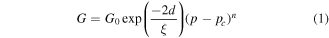
A strip of NP monolayer with a width of 1 ∼ 2 μm is situated on the flexible PET substrate by means of convective assembly at the confined contact angle, whose mechanism was described in our previous work [34] and reproduced in figure 1(a). Two kinds of Au NPs, the nanosphere (NS) with a smooth surface and the nano-urchin (NU) with a rough surface, are hexagonally packed on the PET substrate within a short range, as shown in figures 1(b)–(f) and figure S1. The crevice size can be as small as ∼1 nm in both the Au NS and NU arrays (figures 1(d) and (f)). Although physical touch is visible amongst some neighboring Au NPs, chemical bonding or welding does not occur, as revealed by the temperature effect of the electrical properties shown in figures 2(a) and (c). The relative change of resistance value of the NU monolayer monotonously declines from 2.206 to 1.152 MΩ when the temperature rises from 270 to 350 K. The average temperature coefficient of resistance (TCR) is −0.006 Ω/K within the temperature range of 270–350 K. Meanwhile, the relative change of resistance value of the NS monolayer with the increasing of temperature declines and its TCR is −0.01 Ω K-1 within the temperature range of 270–350 K. (see figure 2(a)). Note that polycrystalline Au film has a positive TCR (figure 2(a), inset), whose average TCR is 0.001 Ω K-1 within the same temperature range [37]. Sign change in TCR is a good indicator that tiny crevices have been embedded into the NP monolayer. Even though surface morphologies of the NP monolayer as shown in figures 1(d) and (f) suggest the existence of some kinds of physical contact, actual electrical contact between the NPs is probably at atomic level. According to previous investigation on granular film, tunneling across a potential barrier is thermally activated. That is, electron tunneling becomes easier at higher temperature. By contrast, a granular Au film with a positive TCR primarily results from electron scattering by the phonon [38].

Figure 1. The morphology of Au NS monolayer and Au NU monolayer fabricated by convective assembly. (a) Optical micrograph of a NP strip prepared by convective assembly (yellow line). Inset: schematic illustration to assemble one strip of Au NP. (b) Top view of the SEM image of Au NS monolayer with a width of 1∼2 μm. (c)–(d) TEM images with different magnifications of Au NS with a smooth surface. (e)–(f) TEM images with different magnifications of Au NU with a rough surface.
Download figure:
Standard image High-resolution image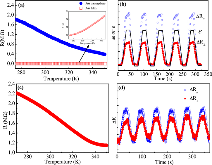
Figure 2. The behavior of tunneling within sub-nm scale crevice characterized by the electrical responses of the NS and NU monolayer. (a) Normalized resistance value of Au NS monolayer (blue line) and Au thin film (red line) as a function of temperature. Inset: relative change of resistance of polycrystalline Au film as a function of temperature. (b) Variation of resistance of a parallel NP strip (blue line) and a perpendicular NP strip (red line) on the same chip when it was cyclically mechanically stimulated (black line). (c) Normalized electrical resistivity of Au NU monolayer as a function of temperature. (d) Variation of resistance of Au NU monolayer of a parallel NP strip (blue line) and a perpendicular NP strip (red line) when it was cyclically bent (ε = 0.012%).
Download figure:
Standard image High-resolution imageTo investigate the anisotropic tunneling within sub-nm scale crevices, electrical conductivity of the NS monolayer is measured in real time. When the flexible substrate is periodically bent convex (loading) and then released (unloading), resistance correspondingly varies in exactly the same cyclic fashion (ε = 0.112%) (see figures 2(b) and (d)). Obviously, the value of ((ΔR/R)//)/((ΔR/R)⊥) of the NS is much larger than that of the NU. It indicates that the conduction property of the NS behaves anisotropically, whereas the NU is nearly isotropic (as shown in figure 2(d)). When mechanical strain is respectively discomposed along the perpendicular and the parallel axes (see figure S3), ΔR/R varies differently with respect to ε. When ε rises from zero to 0.114% as shown in figure 2(d), the value of (ΔR/R)// is 0.12, which is almost double that of (ΔR/R)⊥ as shown in figure 2(c). When ε drops from 0.114% to 0.093%, there is a noticeable difference between (ΔR/R)// and (ΔR/R)⊥, indicating that the conductivity is anisotropic. More importantly, the relative variation of resistance, denoted as ΔR/R, can restore to its original value even when an extremely low mechanical strain is released, as shown in figure S3. The recovered resistance after loading-unloading cycles at low strain level indicates the reliability and high sensitivity of strain sensor. Figures 3(a) and (b) represent the overall variation of the (ΔR/R)// and (ΔR/R)⊥ as a function of ε in convex and concave axes. For the NS monolayer, both the (ΔR/R)// and (ΔR/R)⊥ monotonously increase with the strain going from −0.01 (concave) to 0.01 (convex). When the strain is negative (−0.01), (ΔR/R)// is about 0.41 and (ΔR/R)⊥ is about 0.70. In the presence of positive strain, the value of (ΔR/R)// is much higher than that of (ΔR/R)⊥, especially in the presence of high strain level. For instance, (ΔR/R)// is about 5.18, which is almost five times higher than the (ΔR/R)⊥ (∼0.91), for a strain level of 0.01. For the NU monolayer, the almost identical relation between ΔR/R and ε can be attained in the parallel and perpendicular axes, except for a slight deviation at high strain level. This relationship causes the NU monolayer to have an isotropic response to mechanical strain.
Figure 3. Topography-dependent isotropic tunneling characterized by the electrical responses of the NS monolayer and NU monolayer. (a), (b) Relative resistance variation ΔR/R as a function of horizontal mechanical strain and vertical mechanical strain for the Au NS monolayer and the Au NU monolayer. The red line and blue line are the fitting curves according to equations (3) and (4). (c), (d) The ΔR/R for the Au NS monolayer and Au NU monolayer measured by bending the substrate at orientation angles from zero to 90°.
Download figure:
Standard image High-resolution imageThe results described above indicate that isotropic electron tunneling is dependent on the surface topography of the Au NPs. In this work, most crevices between the neighboring NPs are at sub-nm scale as shown in figure 1 prior to mechanical bending. Therefore, the parameters p and n can be assumed as the constants, implying that the power term in equation (1) that corresponds to the percolation possibility is a constant throughout the entire range of the mechanical stimulus. If one assumes that crevice size changes from d to d + Δd, the strain of the bent substrate is now given as ε = Δd/d. The NP monolayer can be considered as a tunneling network, and its conductivity can be rewritten in terms of ΔR/R:
R1 is the initial resistance in the unstrained state. G1 is the initial conductivity in the unstrained state. G2 is the final conductivity in the tensile state. Substituting equation (1) into equation (2) yields the ΔR/R in parallel axes:
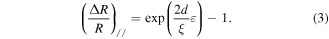
If anisotropic resistivity is considered during mechanical bending, anisotropic factor B can be introduced into equation (3) to account for the orientation dependence of ΔR/R. Hence, the ΔR/R in the perpendicular axes can be described as:
Therefore, one can fit experimental data by simultaneously using equations (3) and (4). For an NS monolayer, B has a value of about 0.37 (The detailed derivation is compiled in the supplementary material). To verify the anisotropic tunneling between the straining arrays, the ΔR/R is measured by bending the PET substrate at orientation angles from zero to 90° in the same strained condition (ε = 0.637%). In the convex state, the relative variation of resistance (ΔR/R) decreases from 2.1 to 0.6 with the increase in the angle. Meanwhile, the ΔR/R drops from 0.63 to 0.26 with the increase in the angle in the concave state. Therefore, the ΔR/R exhibits an angle-dependent property as shown in figure 3(c). By comparison, the fitting B is 0.88 for the NU monolayer. Besides, when the angle increases from zero to 90°, the ΔR/R of the NU monolayer remains almost unchanged like a constant (∼1.3) in the convex state and the concave state (∼0.58) as shown in figure 3(d). The result here indicates that the ΔR/R has angle-independent property in the case of the NU.
Transport anisotropy in many disordered systems is of fundamental concern. Ultrathin granular film, as a classical system, has been commercialized in the electronics industry [25, 39, 40]. The anisotropic resistivity depends on the predictable evolution of geometrical parameters along different orientations to supply the mechanical strain [16, 41]. In this system, the resistivity does not rely on the electron tunneling between the neighboring conductors [25, 39, 40]. However, electron transport of both the isolated metallic islands and the assembled NP arrays relies on electron tunneling between the neighboring islands or NPs. This intrinsic mechanism has been experimentally verified by in situ tailoring the crevice size and tunneling barrier. The former can be reliably tuned by mechanical bending [24, 40], and the latter is tuned not only by mechanical bending, but by changing the ambient environment [28, 37]. In our previous investigations, the isolated metallic islands are exposed to the atmosphere with different humidity levels, confirming the evolution of tunneling barrier [28, 35].
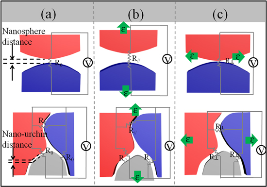
To understand the distinct tunneling behaviors within the NS and NU monolayers, a schematic is illustrated in figure 4. The minimum crevice (d) of two NPs is defined as the tunneling path of the NS/NU as shown in figure 4(a). Each NP is connected with its nearest neighbors to form a resistor with a resistance of R0 ∼ e2d/ξ. As indicated in figures 4(b) and (c), when mechanical strain is respectively decomposed along the perpendicular and parallel axes, the ε// of the planar NS arrays is larger than ε⊥ ≈ νε//. The tunneling path does not change when there is face-to-face contact and the tunneling distance is only affected by Poisson's ratio (see figure S4). Therefore, the planar NS arrays (B = 0.37) exhibit anisotropic conductivity in response to the strain, which is close to a previous report on Poisson's ratio of 0.32 in NP monolayer [39, 42, 43]. Thus, the tunneling resistance dependent on the crevice size exhibits anisotropic behavior ((ΔR/R)// > (ΔR/R)⊥). On the other hand, nearly isotropic tunneling appears in the NU monolayer, which can be attributed to the irregular surface profiles. Surface pikes in the NU monolayer are randomly distributed in space, indicating the crevice variation of two NUs along the direction of applied strain can be statistically identical (see figure S4). The equivalent tunneling paths are also randomly distributed in the substrate plane when the substrate is bent. In this case, the tunneling path in the NU arrays does not depend on the orientation to supply the mechanical strain. Therefore, the B in the NU array is 0.88, exhibiting isotropic tunneling in response to mechanical strain exerted from different orientations. Hence, the relative variation of electrical resistance caused by the disconnection of each NP surface presents isotropic character ((ΔR/R)// ≈ (ΔR/R)⊥).
Figure 4. The variation of the (ΔR/R)// and (ΔR/R)⊥ with a function of ε in convex axes. (a) The behavior of Au NS monolayer and Au NU monolayer in the unstrained stages. (b), (c) The behavior of Au NS monolayer and Au NU monolayer in the stages of tensile strain along the parallel and perpendicular axes.
Download figure:
Standard image High-resolution image
Topography-dependent isotropic tunneling observed in this work will be an advantage to design reliable flexible devices. Because the electrical resistance of the NU arrays is not sensitive to the direction of the applied mechanical strain, one can explore their applications in some flexible electronics with high precision, such as finger-touching sensor [10], and acoustic vibration with small amplitude [11]. In addition, if the NS array contains the crevice at sub-nm scale, plasmonic performance will sensitively rely on electron tunneling within the crevices. Its optical spectrum should be sensitive to the polarized direction of incident light. If isotropic tunneling is obtained in the NU array, the identical spectrum is not dependent on the polarized direction of incident light. Strain gauge with high sensitivity and reliability can be designed by considering tunable and isotropic tunneling by monitoring its plasmonic property [44].
Conclusion
In conclusion, the assembled NP monolayers with both spherical contour and urchin-like contour are configured to clarify electron tunneling mechanism that depends on the orientation of the applied mechanical strain. Different from the spherical NPs, electron tunneling within urchin-like NPs exhibits the nearly isotropic response to the compressive and tensile strains with different loading orientation. Topography-dependent isotropic tunneling results from the randomly spatial interlocking between the pikes of urchin-like NPs subjected to external mechanical stimulus. The conversion mechanism from anisotropic to isotropic offers one unique road to design flexible electronics with high precision including finger-touching sensor and acoustic vibrometer in the future.
Acknowledgments
This work was partially supported by Innovation Funding of HUST for International Collaborations (2014ZZGH018), the Specialized Research Fund for the Doctoral Program of Higher Education (20130142120089), and the National Natural Science Foundation of China (51371084 and 91545131). Microstructure characterizations were carried out by the State Key Laboratory of MPDMT in HUST.
Conflict of interest
The authors declare no competing financial interest.