
Abstract
Resistive random access memory (RRAM) is considered an attractive candidate for next generation memory devices due to its competitive scalability, low-power operation and high switching speed. The technology however, still faces several challenges that overall prohibit its industrial translation, such as low yields, large switching variability and ultimately hard breakdown due to long-term operation or high-voltage biasing. The latter issue is of particular interest, because it ultimately leads to device failure. In this work, we have investigated the physicochemical changes that occur within RRAM devices as a consequence of soft and hard breakdown by combining full-field transmission x-ray microscopy with soft x-ray spectroscopic analysis performed on lamella samples. The high lateral resolution of this technique (down to 25 nm) allows the investigation of localized nanometric areas underneath permanent damage of the metal top electrode. Results show that devices after hard breakdown present discontinuity in the active layer, Pt inclusions and the formation of crystalline phases such as rutile, which indicates that the temperature increased locally up to 1000 K.
Export citation and abstract BibTeX RIS

Original content from this work may be used under the terms of the Creative Commons Attribution 3.0 licence. Any further distribution of this work must maintain attribution to the author(s) and the title of the work, journal citation and DOI.
1. Introduction
Resistive random access memory (RRAM) devices, also known as memristors, are typically metal–insulator–metal heterostructures, which are often based on transition-metal-oxide thin films. RRAM is considered a prominent candidate for next generation memory due to the device's simple structure, low power consumption, high-density integration and high-speed operation (<10 ns) [1]. RRAM cells exhibit resistive switching (RS), meaning that they can toggle between high-resistive states (HRS or OFF) and low-resistive states (LRS or ON) under appropriate biasing. Such ON/OFF cycles can be repeated several times before the device's eventual failure [2, 3]. The dynamics of RRAM cells are still not well understood despite the several mechanisms that have been reported to date. One of the most popular is the filament-type, which is based on the formation and migration of defects (e.g. oxygen vacancies or titanium interstitials) along the metal-oxide thin film that result in the formation of highly conductive nanofilaments (CFs) of reduced oxide phases perpendicular to the electrodes [4–6]. Yet, so far, very limited direct experimental evidence of the nanoscale changes that occur in the oxide film, as a consequence of switching, have been reported [7–11]. In particular, there is a lack of knowledge of changes that occur in the oxide when the device undergoes permanent failure.
It has been observed that RS in RRAM devices is often associated with morphological changes of the metallic top electrode (TE) [4, 12–17]. Early reports on such defects have existed since the 1970s [18, 19], when the theory of memristors was first formalised by Chua [20, 21]. Minor deformations typically denote a reversible soft-breakdown (SB) mechanism [4]. However, after the application of high voltages or a large number of switching cycles such protrusions accumulate irreversibly until the device is damaged, i.e. it is no longer possible to alter the device's memory state, also known as hard breakdown (HB) [22]. These dramatic events that cause permanent failure of the devices are one of the major issues that prevent RRAM scalability and commercialization [23]. The causes of these morphological changes are still controversial and have been ascribed to different mechanisms such as solid electrolysis and electrode melting [12]. As these indicate dramatic changes due to RS, it is essential to perform an accurate analysis of the defect area, in particular of the oxide structure underneath the TE defect that can shine more light towards the underlying RS and failure mechanism.
Recently, Lee et al [24] have investigated the physical mechanisms that cause fatal damage to nanometric thick top electrodes in RRAM devices. By employing a computer simulation based on a percolation model, they ascribed the fatal electrical breakdown to the large voltage stress and current flow caused by the formation of many CFs. However, atomic-scale studies of chemical changes occurring in the active layer and at the interfaces during SB and HB are still limited. In particular, there is lack of information on the specific oxide phases that form underneath the TE damage [25, 26].
In this work, we present an atomic-scale chemical investigation of changes that occur along a cross-section of a Pt/TiOx/Pt/Cr/Si/SiO2-based device after SB and HB switching underneath a TE defect using soft x-ray spectromicroscopy, a synchrotron-based technique that measures near-edge x-ray absorption fine structure (NEXAFS) spectra at high spatial resolution in a full-field transmission x-ray microscopy (TXM). Recently, we have presented the results obtained using this technique applied to a functioning Pt/TiOx/Pt pre-switched device in LRS. The device was switched by applying a relative low voltage in the range ±1.5 V. Spatial resolution and chemical characterization of distinct TiOx phases along the cross-section were performed [27]. In this case, only a very small defect of the TE was observed. Results showed the formation of voids underneath this defect, with localized reduction of the pristine TiOx phase and crystallization to anatase and rutile in regions adjacent to the voids. In this manuscript, we have used the same experimental technique to investigate the cross-section of devices after SB and HB, switched using higher voltages compared to the functioning LRS device, where much more extensive damage of the TE was observed, with the final aim to study the failure mechanism of RRAM devices. Different from our previous work, several Pt inclusions were observed into the active oxide underneath the extended defect of the devices after both SB and HB, which could be responsible for the failure mechanism that eventually occurs in these devices.
2. Experimental section
2.1. Device preparation
The Pt/TiOx/Pt/Cr-based devices were fabricated on an oxidized (200 nm SiO2) 6 inches Si wafer. A bottom electrode (BE) and TE were fabricated using conventional optical lithography, and electron-beam evaporation followed by a lift-off process, with the BE and TE composed of Cr/Pt (3 nm /30 nm) and Pt (30 nm), respectively. The Cr film served as the adhesive layer for the Pt BE. A 50 nm TiOx layer was then deposited using reactive sputtering from a Ti metal target with the following settings: 8 sccm O2, 35 sccm Ar, 2 kW at the cathode, and 15 sccm O2 and 2 kW at the additional plasma source. The active layer area was patterned using optical lithography and the lift-off process.
2.2. Electrical characterization of devices
Electrical biasing of the devices has been carried out through voltage sweeping both for assessing and modifying their resistive states. Passive resistive state assessment of the device under test was carried out via low voltage (within +/−2 V), non-invasive voltage sweeps, whilst RS was induced through the application of more aggressive, high-voltage sweeps. All voltage biasing was carried out under current compliance protection. The compliance current levels were determined on an ad hoc basis. All sweeping was performed using a Keithley 4200 electrical characterization instrument.
2.3. Atomic force microscopy (AFM)
AFM maps were acquired with a MultiMode Nanoscope V AFM (Veeco Metrology Group) in contact mode using Pt/Ir coated Si tips with a cantilever spring constant of 0.2 N m−1 and a nominal radius of 12 nm (Bruker, SCM-PIC).
2.4. Focused ion-beam scanning electron microscopy (BFIB-SEM)
A dual-beam BFIB-SEM system (Zeiss NVision 40 FIB/FEGSEM) equipped with a gas injection system was used to record SEM images and for cutting FIB cross-sections. SEM images were recorded at an accelerating voltage of 5 kV. Prior to performing FIB cross-sections, an electron-beam-induced tungsten protective layer was deposited on the top of the electrodes in order to minimize damage caused by the gallium ions in the subsequent cutting steps. After extraction, the thickness of the lamella is further decreased to allow x-ray transmission by low-energy ion polishing at a low incident angle until a thickness of 40–70 nm is achieved.
2.5. TXM-NEXAFS
The TXM-NEXAFS study was performed at the undulator beamline U41-FSGM at the BESSY II electron storage ring operated by the Helmholtz-Zentrum Berlin. The TXM has a spatial resolution of 25 nm and spectral resolution of E/ΔE = 10 000 [28]. Sequences (stacks) of x-ray images were acquired at closely spaced photon energies (0.1 eV steps) using a TXM, in the Ti 2p (450–485 eV) and O 1s (525–555 eV) energy range. Image size is 1340 × 1300 pixels corresponding to 5 nm per pixel. Each image was taken with the sample at the proper focus position to optimize the spatial resolution [29]. The stack of all images was created followed by automatic alignment using Fourier cross-correlation techniques in aXis2000 and in Stack_Analyze [30]. Each stack, consisting of 1053 images over the Ti 2p energy range and 351 images over the O 1s energy range, was carefully aligned using a cross-correlation iteration process until the image shift was less than ±0.6 pixels (±3 nm) across the entire energy range. The alignment of images is required to correct for lateral motion of the x-ray beam on the sample [29]. The incident x-ray intensity (Io) for each stack was obtained from an internal region of each stack (off the FIB section) and used to convert the aligned stack from transmission to optical density (OD = −log[I(E)/Io(E)]). Ti 2p and O 1s spectra were then extracted from the stack. Spectra can be obtained from regions as small as the spatial resolution of the microscope (25 nm). A detailed analysis involving extraction of the x-ray absorption spectra of specific regions of interest was performed [31, 32] using aXis2000 software[30].
2.6. Materials and methods of choice
Several transition-metal oxides are of particular interest for RRAM, in particular TaOx [33] and HfOx [34] due to their simple reduction dynamics. On the other hand, TiOx provides wider opportunities for multi-state memory capacity due to the intrinsic variety of possible chemical phases. A previous work by Kwon et al [4] based on high-resolution transmission electron microscopy (HRTEM) study and interpretation of electron diffraction patterns, identified Ti4O7 as the structure of CFs buried underneath a TE deformation in a TiO2 based RRAM device. However, HRTEM requires the use of high-energy electron beam (200–300 kV), which could induce sample crystallization and effectively alter the physical–chemical state of the film during irradiation. Furthermore, electron diffraction requires crystals to be aligned in specific orientations with respect to the beam for unambiguously capturing distinct diffraction patterns [4]. Previous works have shown that synchrotron radiation-based techniques are powerful tools for nanoscale characterization of changes in RRAM devices [7, 10, 11, 15–17, 35, 36]. TXM-NEXAFS allowed us to simultaneously perform imaging and spectroscopy for investigating morphological changes in the film as well as performing chemical analysis at nanometer scale of localized regions, respectively. Identification of distinct TiOx phases formed in localized regions underneath the TE damage has been achieved using Ti 2p and O 1s NEXAFS spectra. The identification is based on fingerprint methods, avoiding the difficulties imposed via multiple scattering effects and/or the presence of diffraction spots from other TiO2 phases and/or metallic electrodes when employing electron diffraction.
3. Results
The RRAM devices investigated here are based on a Pt (30 nm) TE/TiOx active layer (50 nm)/Pt (30 nm) BE stack fabricated on a SiO2/Si substrate, as schematically represented in figure 1(a). Figure 1(b) shows a single device with an active junction of 40 × 40 μm2. The value of x in TiOx was determined to be 1.95 by x-ray photoelectron spectroscopy (data not shown).
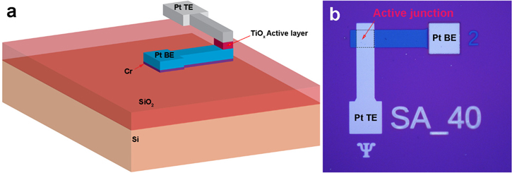
Figure 1. TiOx RRAM-based device: (a) schematic of the device's architecture; (b) optical image of a single device with an active junction of 40 × 40 μm2.
Download figure:
Standard image High-resolution image3.1. Electrical characterization
Two devices were electrically characterized using voltage sweeping and the corresponding current–voltage (I–V) curves are reported in figure 2. The first device was electroformed at +5.7 V (inset of figure 2(a), compliance current 10 mA) and subsequently underwent a single switching cycle (figure 2(a)). First, a negative sweep caused switching from an LRS to an HRS at approximately −5.0 V. Next, a positive voltage sweep caused the device to switch back to the original LRS. Despite the high voltages employed, the device successfully switched between ohmic and non-linear regimes reversibly, as shown in the I–V curve of figure 2(a) and it will be hereafter called Dev_SB. The second device was formed at 12.0 V and subsequently cycled 20 times when breakdown occurred as shown in the I–V curve in figure 2(b). The device will be hereafter called Dev_HB. Figure 2 b) displays only four loops out of the 20: electroforming (inset), 1st, 8th and the 20th switching cycles where breakdown occurs. It has to be noted that the voltages/currents used to reach HB are somewhat higher than the usual values used in our commonly used operational devices due to the higher thickness of the TiOx film (50 nm), chosen considering the spot size of the TXM-NEXAFS beam. Significant cycle-to-cycle variations in switching voltages (+3.5 , −2.5 V and +9.0, −15.0 V for cycles 1 and 8 respectively) were observed. A compliance current of 10 mA was used during forming and raised to 100 mA during switching; a value that was never reached. Throughout the electrical characterization, voltages as high as ±15 V were employed in order to account for the 50 nm active layer thickness employed in this experiment. Even if quite different electroforming voltages were required to form the Dev_SB and Dev_HB, the qualitative aspects of the switching behavior were broadly maintained.

Figure 2. I–V characteristics of (a) Dev_SB and (b) and Dev_HB. Insets: electroforming steps. Each switching cycle consists of a negative polarity sweep followed by a positive polarity sweep.
Download figure:
Standard image High-resolution image3.2. SB sample
Several studies have shown that protrusions of the TE (both in the center [8, 16, 37–39] and at the rim [16, 38]) could indicate possible critical regions of the film responsible for the RS. The AFM image of the Dev_SB viewed from the TE, reported in figure 3(a), shows two defects: a 300 nm high isolated protrusion in the center of the active area and an extended defect at the rim of the Pt TE in the top right region. We have only investigated the extended defect at the rim of the TE as this study is mainly focused on the understanding of device failure. Therefore, the most damaged area is likely to give more detailed information on the breakdown mechanism of devices. Moreover, it has been recently reported that this position could give significant information on the RS being a preferred reduction site since it is a three-phase contact site (oxide, metal and ambient atmosphere) [36]. The detailed AFM image of the extended defect at the edge of the electrode, reported in figure 3(b), shows that the Pt TE forms several protrusions up to 400 nm high. The corresponding SEM images are reported in figures 3(c) and (d). The detailed SEM image (figure 3(d)), shows that the TE is protruded, forming several rounded features, suggesting melting of the Pt. It has to be noted that damage at the rim of the TE has been previously observed in similar devices [12].

Figure 3. AFM (a-b) and SEM (c-d) images of the Dev_SB viewed from the TE. The red line in (a) indicates the region where the FIB lamella was cut.
Download figure:
Standard image High-resolution imageOptical images taken before and after electrical switching (figure S.I.1), prove that central and edge deformations were not present in the pristine device and are, therefore, due to the RS. In particular, it has been suggested that these irreversible morphological deformations are caused by the development of oxygen gas at the interface TiOx/TE due to the formation of reduced TiOx phases which aggregate in CFs according to the following reaction [40, 41]:

The temperature in the localized conductive nanofilaments increases significantly due to Joule heating causing the Pt to melt [12, 40].
In order to visualize and characterise the area buried underneath the damaged TE, an FIB lamella was extracted along the red line indicated in figure 3(a) using the lift-out technique as shown in figure S.I.2(a). Details of the cross-sectional lamella (figure S.I.2(b)), show that under the identified protrusion, the TE bulges and partially aggregates in rounded features connecting the BE and TE. The TE is lifted from its original position, supporting the argument that the protrusions were caused by O2 gas escaping through the weakest point of the TE, the rim, in agreement with previous observations [40]. The SEM image of the lamella thinned for electron transmission, reported in figure S.I.2(c), shows that the damaged region is also lifted from the support as indicated by the bright area in the inset image.
In order to investigate chemical changes across the TiOx layer as a consequence of SB switching, TXM-NEXAFS measurements were performed on the FIB cross-section of the device. In figure 4, x-ray images of the lamellae at 450 eV (below the Ti 2p edge), 465 eV (on the strongest Ti 2p absorption peak), 525 eV (below the O 1s edge) and 531 eV (on the strongest O 1s absorption peak) are presented.
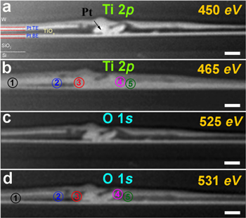
Figure 4. Optical density TXM micrographs of Dev_SB obtained at the Ti 2p absorption edge with photon energy of 450 and 465 eV and at the O 1 s absorption edge with photon energy of 525 and 531 eV. Scale bar = 200 nm.
Download figure:
Standard image High-resolution imageThe stack of layers i.e. Pt/TiOx/Pt/SiO2/Si are highlighted in figure 4(a). By examining the Ti 2p and O 1s image sequences at different energies, we can spatially resolve the location of the regions containing Ti and O species, respectively, as the contrast of the image changes in correspondence with changes in the Ti and O absorption peak intensities. At 450 eV (figure 4(a)), the TiOx layer appears dark as Ti does not absorb at this energy. At 465 eV (figure 4(b)), the same layer appears bright due to the strong absorption of Ti. Therefore, the regions that appear dark at 450 eV, but bright at 465 eV, correspond to Ti-containing areas. Similarly, for the O 1s at 525 eV (figure 4(c)), the TiOx layer appears dark as O does not absorb at this energy and bright at 531 eV (figure 4(d)), due to the strong absorption of O. Therefore, the regions that appear dark at 525 eV, but bright at 531 eV, correspond to O-containing areas. Different from what is observed in the cross-section of functioning devices in the LRS [27] a main Pt agglomeration is observed underneath the defect, exactly underneath the rim of the TE, as indicated in figure 4(a). Electrochemical dissolution of Pt in oxides under high electric fields in RRAM cells has already been reported by Yang et al [42]. Spatially localized NEXAFS spectra at the Ti 2p and at the O 1s absorption edges were then extracted from various regions of the TiOx film area in both sides of the Pt agglomeration. Five regions of interest (ROI) were identified, indicated in figures 4(b) and (d) by numbered circles. The Ti 2p and O 1s x-ray absorption spectra extracted from each of these localized regions are reported in figures 5(a) and (b), respectively. Different spectral features at both Ti and O edges appear for the different ROI, indicating changes from the pristine structure (as-deposited TiOx).
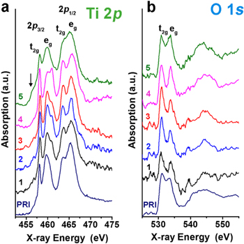
Figure 5. NEXAFS Ti 2p (a) and O 1s (b) spectra of Dev_SB extracted from the regions circled in the x-ray images of figures 4(b) and (d).
Download figure:
Standard image High-resolution imageThe Ti 2p spectrum presents distinct features for the different polymorph phase of crystalline TiO2 and for amorphous TiO2 [43]. The Ti 2p spectrum of the pristine sample (figure 5(a)) shows broad peaks, and no splitting of the (2p3/2, eg) peak. These features are consistent with a high structural disorder caused by a range of bond angles and lengths as expected for amorphous TiOx. Ti 2p spectrum of region 5, on the right side of the Pt agglomeration, exhibits broad peaks as an amorphous structure. In addition, an energy shoulder appears at around 456 eV, which is consistent with the presence of a partially reduced phase containing Ti3+ [38]. The presence of a mixture of Ti3+ and Ti4+ could contribute to the fact that the peaks are slightly broader compared to the pristine sample, as inferred from the reduced 2p3/2 and 2p1/2 peak-to-valley ratio. In addition, spectra of phases containing Ti3+ show broader features compared to the pure Ti4+ phases, because of the binding energies of the Ti3+ levels and overlapping and increasing numbers of allowed transitions in the Ti3+ spectra [44]. Spectra from regions 1–4, all extracted from the TiOx areas underneath the damaged TE show sharper features with significant variation in shape, clearly indicating significant changes in the chemical structure of TiOx. In particular, all spectra show splitting of the (2p3/2, eg) peak, which indicates distortion of the TiO6 octahedra [45]. The relative intensities of these two peaks depend on the particular type of octahedral distortion, and therefore, on the particular polymorphic form of TiO2. In the spectrum of region 4, very close to the Pt agglomeration, the relative intensities of the split (2p3/2, eg) peak are different, being higher for the peak at higher energy. This is typical of the TiO2 rutile phase, which has tetragonal distortion of the TiO6 octahedra [43, 46]. In the spectra of regions 1–3, the relative intensity of the split (2p3/2, eg) peak is the opposite to that in rutile, with the intensity being higher for the peak at lower energy. This profile is typical of anatase [45, 47]. The peak-to-valley ratio of the 2p1/2 peak in regions 2 and 3, where the TiOx film is delaminated from the Pt BE, are particularly high, indicating a high degree of crystallinity. In contrast, 2p1/2 peaks of region 1, where the TiOx layer is not yet delaminated, are much broader, indicating a lower degree of crystallinity.
If Ti 2p spectra give a clear indication of the phases formed, while O 1s spectra, shown in figure 5(b), are more difficult to interpret. Variations between the selected regions of interest are less evident at the O 1s, as the change in structure of TiOx has less influence on O 1s than Ti 2p spectra. O 1s spectra of the pristine device show broad and smooth spectral features typical of amorphous TiOx. Moreover, the dip between the (O 1s, t2g) and (O 1s, eg) peaks is shallow compared to the spectra of all the other regions and their energy difference, which is often used to evaluate crystal field splitting, it is smaller and typical of disordered materials (2.0 eV) [48]. In the spectra extracted from regions 1–4, the eg and t2g peaks appear more defined and intense. The energy gap between eg and t2g in regions 1–4 is ∼3.0 eV, a value reported for both anatase and rutile phases [43]. In region 5, the dip between eg and t2g is less intense, which is in agreement with the Ti edge that shows broad peaks, as an amorphous structure. It has to be noted that no signal due to the presence of oxygen vacancies is observed beneath the O 1s jump, as expected for a reduced TiOx. This could be ascribed to the fact that only a small amount of Ti4+ is reduced to Ti3+ so the amount of Ti3+ might not be high enough to generate an observable peak. In support of this statement, in the work of Strachan et al [38], where a shoulder at 456 eV of similar intensity corresponding to Ti3+ was observed in the Ti 2p spectrum, no signal due to defect state was observed in the O 1s spectrum.
3.3. HB sample
We now consider the sample switched for 20 cycles until HB. Figure 6(a) depicts the SEM image of Dev_HB viewed from the TE taken using a conventional secondary electron detector (EHT = 5 kV).

Figure 6. (a) SEM image of Dev_HB view from the TE with the region where the lamella was cut (red line); (b) magnified SEM image of lamella-cut region; (c) optical and (d) AFM images of the region inside the yellow square in (a).
Download figure:
Standard image High-resolution imageMajor damage of the TE occurred, with tree branch-like patterns spreading over the junction area and peeled-off metal as a result of heating and oxygen pressure. A similar branch-like pattern of local defects has already been observed as a result of electrical conduction through thin sandwich structures [18]. A complete detachment of the TE from the active area is observed on the right rim of the junction. Very similar morphological changes with the formation of dendrite-like structures were observed by Skaja et al [49] in the TE of Pt/Ta2O5/Ta devices. As evident from the magnified SEM (figure 6(b)) and optical (figure 6(c)) images, several parts of the Pt TE are delaminated. However, the BE is still mainly unaffected as proved by the dark blue regions observed in the optical image underneath the delaminated Pt TE. The AFM images reported in figure 6(d) and figure S.I.3(a), show that the Pt protrusions are mostly 100–150 nm high with a few features up to about 400 nm. The deflection error image, reported in figure S.I.3(b), reveals additional details of the defects, such as the 2 μm elongated crater shown in the inset.
An FIB lamella was cut in the region highlighted by the red line in figure 6(a). Details of the lamella extraction are reported in figure S.I.4(a). Different from Dev_SB, cross-section views reported in figure S.I.4(b) and figure S.I.4(c), show several Pt inclusions lying on the BE. In particular, a main Pt aggregate about 200 nm wide protrudes across the oxide film, marked in figure 7(a). It has to be noted that in this device, the number of Pt protrusions across the active oxide is much higher than in Dev_SB.

Figure 7. Optical density TXM micrographs of Dev_HB obtained at the Ti 2p absorption edge with photon energy of 450 eV (a) and 465 eV (b) and at the O 1s absorption edge with photon energy of 525 eV (c) and 531 eV (d). Scale bar = 200 nm.
Download figure:
Standard image High-resolution imageTXM micrographs at the Ti 2p (450 and 465 eV) and at the O 1s (525 and 531 eV) are reported in figure 7. As described previously for the Dev_SB, regions that appear dark at 450 and 525 eV and bright at 465 and 531 eV, correspond to Ti- and O-containing areas, respectively. NEXAFS spectra at the Ti 2p and the O 1s were extracted from the TiOx film area. Due to the extent of the damage, ten ROI were identified, indicated in figures 7(b) and (d) by numbered circles.
The Ti 2p and O 1s x-ray absorption spectra extracted from each of these localized regions are reported in figures 8(a) and (b), respectively.
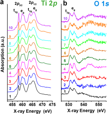
Figure 8. NEXAFS Ti 2p (a) and O 1s (b) spectra of Dev_HB extracted from the regions circled in the x-ray images of figures 7(b) and (d).
Download figure:
Standard image High-resolution imageLet us first consider the Ti 2p spectra. As observed in the case of Dev_SB, significant spectral variations are observed in different regions. Region 1, extracted from an unaffected area, shows mainly amorphous features. Regions 2, 3, 6, 7, 8 and 10 show crystalline features typical of anatase phase as the first peak of the 2p3/2 eg splitting has higher intensity than the second. Region 4, very close to the main Pt agglomeration, again shows crystalline features, but the intensity of the 2p3/2 eg splitting is comparable. This particular (2p3/2, eg) profile has been reported for orthorhombic-like phases such as TiO2-II [47] and brookite [46]. However, the authors cannot exclude the possibility that such a profile could be due to the simultaneous contribution of anatase and rutile. Finally, in regions 5 and 9, which are close to the main defects, the first peak of the 2p3/2 eg splitting has lower intensity than the second, a feature typical of rutile phase. Spectra at the O 1s edge are more difficult to interpret. However, it is confirmed that the pristine sample has broader features compared to the highly crystalline phases.
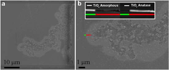
It has been previously shown that the main TE defects (such as craters or protrusions) are typically surrounded by broad areas with scattered surface residue, which has moderate conductivity [25, 50]. We have observed the presence of a halo surrounding the tree-like defect by imaging the TE using a SEM in-lens detector (figures 9(a) and (b)).
Figure 9. SEM images of Dev_HB obtained with an in-lens detector (EHT = 1 kV).
Download figure:
Standard image High-resolution image
The conventional secondary electron detector (used for the image shown in figure 6(a)) is positioned outside the lens system and it is more bulk sensitive. The in-lens detector is positioned in the optical axis in the SEM column and has high surface sensitivity as the image is formed by low-energy electrons. Therefore, the in-lens image contains direct information of the sample surface. The contrast difference between images taken using a conventional secondary electron detector and an in-lens one can be clearly distinguished and different features are observed. In figures 9(a) and (b), two areas with different brightness can be distinguished, the brightest area forming a halo around the defect. Different brightness could be related to difference in the work function (e.g. electronic variations) of the Pt TE in that area. Kelvin probe force microscopy (KPFM) measurement, reported in figure S.I.5, indicates that there is a difference in work function between the heavily damaged area and the undamaged electrode. However, the change in work function in the halo area is not clear. Further analysis is required in order to clarify this point. It has to be noted that other factors affecting the Pt TE in that area could cause differences in brightness such as recrystallization or a cleaner surface due to Joule heating. Chemical characterization of the oxide film underneath the two areas was performed using TXM-NEXAFS chemical mapping. In the inset of figure 9(b), the FIB lamella cut along the green (outside the halo) and red (inside the halo) regions is presented, showing the cross-sections of the film underneath both areas. Chemical maps were generated using the components corresponding to the optimal fits, TiOx amorphous and TiO2 anatase, represented as white regions in the inset in figure 9(b). While the region outside the halo corresponds to amorphous TiOx, as expected, the region underneath the halo has crystallized to anatase.
4. Discussion
The aim of this work is to shed light on the failure mechanism of RRAM devices. It has been proposed that failure in RRAM devices occurs by two different mechanisms: electrical dielectric breakdown or thermally assisted dielectric breakdown [24]. The former is purely due to electronic processes, whereas the latter is mainly caused by Joule heating [51]. This study shows that underneath the TE damaged regions, the TiOx layer undergoes crystallization from the initial amorphous state and that the Pt electrode diffuses in several regions of the film with the formation of voids in both cases of SB and HB. Crystalline phases such as anatase were observed in several regions of both Dev_SB and Dev_HB, whereas rutile phase was observed only in fewer localized areas. Reduced Ti3+ was only observed in Dev_SB. The presence of reduced titanium suggests that prior to the breakdown, a CF was formed in this area, which is believed to be formed by the reduced TiOx phases. It is interesting to note that the rutile phase in Dev_SB is observed in a region very close to the reduced area containing Ti3+ (region 5). It was previously shown that by annealing a TiO2 amorphous film, the anatase phase is formed first, because of energy surface minimization around 650 K [52]. Formation of rutile only occurs after further annealing at higher temperatures, around 1000 K [53]. These results suggest that the temperature increased in all regions to at least 650 K and only in a few localized areas where rutile is present, did the temperature reach 1000 K. The high current density flowing through the CF explains the high increase in temperature in these localized regions, causing crystallization of rutile [36]. This also supports the fact that the regions where rutile was observed, correspond to the areas where CFs were located. The formation of CF could be responsible for the RS of these devices prior to the formation of Pt inclusions that have then caused electric breakdown. It has to be noted that rutile phase appears to be formed only as a side effect of the CF. The high increase in temperature in localized regions up to 1000 K also suggests that cation interstitials could have played a role in the RS mechanism. Oxygen vacancies are often considered the species responsible for RS in transition-metal oxides due to the fact that they have a better mobility than the metal cations at room temperature. However, cation mobility cannot be neglected at higher temperatures. Using scanning tunneling microscopy, Wedig et al [54] gave clear evidence that the cations in thin films of TiOx are mobile under the influence of the electric field and participate in the RS process in competition with oxygen vacancies. Moreover, high cation mobility was also observed in TiO2−x at high temperature [55], but also in thin films grown at room temperature [56]. Therefore, we believe that the mobility of titanium should not be excluded when discussing the switching mechanism in TiO2, in particular when considering the high temperatures caused by Joule heating.
In Dev_HB, the presence of Ti3+ is not evident, but full crystallization of the oxide along with several Pt intrusions (many more than in Dev_SB) are observed. This is in agreement with the more drastic switching conditions that caused a higher extent of the defect on the TE. Crystalline anatase was observed in the halo surrounding the main defect area, where the effect of heating is not localized, but spread across a wide area. The growth of crystalline TiO2 phase requires a significant increase in temperature, which is likely to be induced by the localized Joule heating produced during the switching cycles, suggesting a thermally assisted dielectrical breakdown mechanism. However, crystallization of the initially amorphous active film was also observed in [27], where structural investigation was performed on a functioning device switched into LRS. In that case, as in the present work, reduced TiOx and crystallization of amorphous TiO2 with the formation of anatase, rutile and most probably brookite (or TiO2-II) occurs. The main difference between the functioning LRS device considered in [27] and the Dev_SB reported in this work is the extent of the switching voltage, in the range of ±1.5 V and ±5 V, respectively. Even if, in both devices, the resistance can toggle reversibly between LRS and HRS, the functioning LRS device can be switched for a larger number of cycles, whereas the Dev_SB permanently breaks down after about 20 cycles. TXM-NEXAFS results suggest that this behavior is caused by the formation of Pt intrusions, which accumulate at every switching cycle creating more and more damage until HB. Our working hypothesis is that the switching mechanism is filamentary in nature and dominated by one filament at a time. Therefore, when the device starts cycling, a filament is formed and then broken until SB occurs. At that point, the device experiences some damage, including the Pt intrusions we observed and the switching site is destroyed. At the next cycle, another filament is formed and the device carries on cycling. This procedure repeats and the device gradually accumulates damage. As the device accumulates more and more damage, the switching voltage biases increase until HB. The main difference between the cross-section of the functioning LRS device reported in [27] and that of devices after SB and HB reported in this work, is the extent of the TE defect and the formation of Pt intrusions. Diffusion of Pt in the oxide film could create a short between the BE and TE. Therefore, we believe that these Pt intrusions are actually the final cause of the device failure, which can be considered to be caused by pure electrical dielectric breakdown. Our results provide useful insights into understanding the cause of failure in RRAM devices.
5. Conclusions
TXM-NEXAFS was used to perform morphological analysis and chemical identification of spatially localized areas of TiOx-based RRAM. Changes in the morphology and structure of the initial amorphous TiOx film are observed underneath physical deformations of the Pt TE and in the adjacent area. Pt inclusions and the formation of voids in the TiOx film are observed after both soft (reversible) and hard (irreversible) electrical breakdown. A reduced TiOx phase containing Ti3+ has been observed close to the Pt protrusion in the SB sample, suggesting the location of a CF prior to failure. Crystalline anatase and rutile have been identified in both samples, with rutile being observed in localized areas where the temperature increased up to 1000 K.
Optical images, SEM images and AFM maps of Dev_SB, SEM images of Dev_HB and KPFM of Dev_HB.
Supplementary information
Additional optical/SEM images and AFM/KPFM maps are reported in the supplementary information stacks.iop.org/NANO/27/345705/mmedia
Acknowledgments
The authors wish to thank the HZB, Germany for the allocation of synchrotron radiation beamtime as well as Dr S Werner and Dr K Henzler, both from HZB, for their support during the beamtime. We also wish to acknowledge the support of Dr S Boden, Southampton Nanofabrication Centre, University of Southampton, UK and Dr J C Walker, Faculty of Engineering and the Environment, University of Southampton, UK, for their support during lamellae preparation. The research leading to these results has received funding from the European Community's Seventh Framework Programme (FP7/2007-2013) under grant agreement n 312284. Finally, we wish to acknowledge the financial support of the EPSRC EP/K017829/1 and EU-FP7 RAMP.