

Abstract
Silicon nanowires (SiNWs), fabricated via a top-down approach and then functionalized with biological probes, are used for electrically-based sensing of breast tumor markers. The SiNWs, featuring memristive-like behavior in bare conditions, show, in the presence of biomarkers, modified hysteresis and, more importantly, a voltage memory component, namely a voltage gap. The voltage gap is demonstrated to be a novel and powerful parameter of detection thanks to its high-resolution dependence on charges in proximity of the wire. This unique approach of sensing has never been studied and adopted before. Here, we propose a physical model of the surface electronic transport in Schottky barrier SiNW biosensors, aiming at reproducing and understanding the voltage gap based behavior. The implemented model describes well the experimental I–V characteristics of the device. It also links the modification of the voltage gap to the changing concentration of antigens by showing the decrease of this parameter in response to increasing concentrations of the molecules that are detected with femtomolar resolution in real human samples. Both experiments and simulations highlight the predominant role of the dynamic recombination of the nanowire surface states, with the incoming external charges from bio-species, in the appearance and modification of the voltage gap. Finally, thanks to its compactness, and strict correlation with the physics of the nanodevice, this model can be used to describe and predict the I–V characteristics in other nanostructured devices, for different than antibody-based sensing as well as electronic applications.
Export citation and abstract BibTeX RIS

Original content from this work may be used under the terms of the Creative Commons Attribution 3.0 licence. Any further distribution of this work must maintain attribution to the author(s) and the title of the work, journal citation and DOI.
1. Introduction
The formation of surface dangling bonds is a very well-known phenomenon in silicon device technology. The most common techniques for the fabrication of silicon nanowires (SiNWs) are based on the top-down approach. Top-down fabricated devices rely on lithographic patterning to produce the nanoscale structure, typically by etching. While electron-beam lithography (EBL) leads to the high-resolution definition of nanostructured devices, chemically-assisted etching processes are very aggressive, and result in surface roughness and silicon surface defects [1]. Surface defects are usually associated with dangling bonds defined by missing Si crystal atoms at the surface that leave unsaturated bonds behind them [2]. These unsaturated bonds at the surface give rise to allowed energy states within the forbidden energy gap that are referred to as surface states [3].
Hysteresis in the electrical characteristic of nano-electronic devices, such as carbon nanotubes (CNTs) [4–6] or SiNWs [7, 8], is one of the first indications of the presence of surface traps. Recently, Schottky barrier SiNWs with controlled hysteretic features have been fabricated and used for high-sensitive detection of biomolecules after their functionalization with antibodies [9]. Experimental measurements demonstrated that our SiNW based sensors show a peculiar behavior that is reminiscent of complex memristive and memcapacitive effects, namely resistive and capacitive effects with memory [10–12], when charged species come into contact with their surface. Charged molecules from the surrounding environment determine a sort of memory effect in terms of voltage that has been denoted as voltage gap [13]. Specifically, the voltage gap is defined as the voltage difference between the two current minima in the semi-logarithmic I–V curve of the hysteretic device. It depends on the net charge brought by the molecules to the nanowire surface, thus enabling the sensing of varying concentrations of chemical and biological species [9, 14]. This new class of biosensors based on memristive SiNWs, functionalized with biomolecules, and focused on voltage gap changes as a detection transduction method, takes the name of memristive biosensors [13]. On the other hand, SiNW field-effect transistor (SiNW-FET) sensing techniques, based on electrical measurement of the device conductance as a function of ion or biomolecule concentrations, has been mostly adopted and investigated for biodetection, mainly in an ideal environment, i.e. phosphate buffered saline solution (PBS) [15–20].
In this paper we propose a voltage gap approach with nano-fabricated devices as an alternative detection technique [9, 13, 14]. The experimental data show that this novel sensing method has the potential to overcome the main limitations of low sensitivity in real human samples, such as a tumor extract (TE), with SiNW-FET based sensors [21, 22], thanks to both the increased detection robustness of the voltage gap parameter and the enhanced sensitivity due to another novelty dealing with measurement in air [23], which aims at increasing the Debye screening length [24, 25].
2. Experiments
The SiNWs employed for this work were fabricated on SOI wafer using a top-down process based on a deep reactive ion etching (DRIE) technique described in the experimental section of the supporting information (SI). The scanning electron microscopy (SEM) characterization of the fabricated structures is given in figure 1. Figure 1(a) illustrates the top-view image of a device having a nanowire channel 420 nm long and 35 nm wide. Figure 1(b) shows the tilted-view of the same and shows the vertical stack of nanowires. The nanoscale structures bridge source and drain NiSi contacts that are highlighted in green in both figures for correspondence with the schematic design reported in the SI.
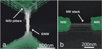
Figure 1. SEM images of a fabricated memristive SiNW device bridging two NiSi contact pads. (a) Top-view SEM image; (b) tilted-view image showing the vertical stack of nanowires.
Download figure:
Standard image High-resolution imageA specific antibody (AB) was linked to the native oxide of the device by means of silane chemistry [26] to functionalize the SiNW, and blocking agents [27] were used to improve the surface specificity of the sensor. Both protocols for surface biofunctionalization and antigen (AG) sensing are described in detail in the experimental section of the SI.
Characterization of the biofunctionalization process was performed both by observation with SEM and fluorescence imaging. In figure 2 we report the SEM micrographs of one of the fabricated devices (a) before and (b) after surface biomodification. From figure 2(b) it is clearly evident the formation of a biolayer of AB around the nanostructure. Figure 3(a) shows the semi-logarithmic Ids–Vds curve of one fabricated SiNW device. The Ids–Vds curve presents a hysteresis loop that is pinched at  V for devices with bare surfaces (black curve), and is clear mark of a memristive system [10, 11]. Once functionalized with ABs, the I–V curve of the sensor changes (figure 3(a)); a non-zero current is now observed when the voltage is swept back to zero (red curve), which is different from the initial condition of zero current at zero voltage. The pinched loop is lost and replaced by a voltage gap defined by the difference in voltage between the crossing points of the forward and backward Vds curves with the x-axis. When the sensor is exposed to a solution of specific AG, then washed, dried and measured, a shrinking of the voltage gap is clearly visible. This shrinking is dependent on the concentration of the target molecule, as demonstrated by the calibration curve reported in figures 3(b) and (c). Details on the sensing protocol and the electrical acquisition are reported in section I of the SI. It is important to observe that all the measurements are performed in air, under fixed relative humidity conditions [9] that are kept constant by continuous monitoring in a sealed measurement chamber. This set-up avoids contamination and creates stable conditions for repeatability of the experiment. Note that a number of control experiments are performed with the aim of defining the electrical noise introduced by interfering species. For example, the effect of silanization on the voltage gap variation has been acquired and, by comparison, estimated to be negligible with respect to the voltage gap modification measured after AB functionalization and AG uptake. Testing the effect of the blocking step with gelatin would lead to further information on the charge-based behavior of the AB–AG complex. In figure 3(b) the experiment consisted of in-air sensing, with the voltage gap technique, of the cancer marker vascular endothelial growth factor (VEGF), diluted in PBS solution in very low concentrations (fM). Figure 3(c) reports the most recent results achieved in the detection of small amount (75–150 fM) of rabbit AG dispersed in the more challenging environment of a breast TE. The TE is prepared directly from patient biopsies (see the SI for details on the TE preparation process), with formation of a cell lysate that is then used for sensing once diluted in PBS, without any kind of filtering. The final concentration of the detected AG in the TE is extremely challenging considering the 100 000 fold mass excess of nonspecific tumor proteins. Data illustrated in figure 3(c) demonstrate the capability of this novel technique in profiling very small concentration changes after interaction with a real biological sample. To the best of our knowledge, the literature reports very few works on immuno-biosensors based on SiNWs capable of measuring femtomoles of AGs in a complex sample such as a TE. Most of the high-sensitive results have been achieved with SiNW-FETs for the detection of RNA with DNA based probes [28]. Very recently, SiNW-FET based in-air immuno-biosensors have been demonstrated as a valid candidate for the highly sensitive detection of cancer markers in real patient samples [23]. However, these results are based on the electrical measurement of the conductance according to the state-of-the-art ISFET technology. In this article we intend to report, for the very first time, an interesting alternative to the femtomolar detection in real breast TEs with memristive immuno-based SiNWs. Memristive nanowires have already been proposed for memory and computation applications but never as ultra-highly sensitive biosensors for detection in breast tumor tissues.
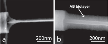
Figure 2. SEM images of a fabricated memristive SiNW (a) before and (b) after the surface biomodification process.
Download figure:
Standard image High-resolution image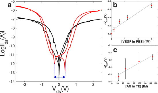
Figure 3. The voltage gap detection approach. (a) The fully pinched hysteresis loop of a just fabricated SiNW (black curve) is lost when its surface is modified with AB (red curve). The adsorption of charged proteins is demonstrated by the augmented current peak and the appearance of a voltage gap. The voltage gap is a parameter of sensing; it decreases as a function of femtomolar concentrations of vascular factors in PBS (b), and as a result of the sensing of AG in the more challenging environment of a breast TE (c). The reported error bars stand for the standard deviation of multiple measures of the same sensor (b), and the standard deviation of the voltage gap acquisitions are related to three similar devices under the same exposure conditions (c).
Download figure:
Standard image High-resolution imageIt is important to observe that the voltage gap strictly depends on the sign of charges carried by molecules from the surrounding environment. Typically, the charge-based behavior of molecular species such as proteins can be predicted by considering their isoelectric point (pI) and by comparing it to the pH conditions of their surrounding liquid matrix. However, when dealing with polyclonal ABs, such as in the case of the present work, the definition of their pI can be very complex. Indeed, polyclonal ABs have no set pI because they are mixtures of various immunoglobulin classes that can alter their net charge and electrical behavior depending on the measurement conditions. Although this complicates the situation, a number of scientific observations have helped to infer the predominant charge-based behavior of the molecules used. Experimental evidence has demonstrated that molecular species carrying a positive net charge are responsible for the appearance and increase of the voltage gap parameter in the Ids–Vds characteristic of the memristive device. On the other hand, species having opposite, negative charge have shown the compensation of this effect by decreasing the voltage gap. Carrara et al have shown that the effect observed in biofunctionalized memristive devices is equivalent to the one of nanostructures without any biofunctionalization, but fabricated with an all-around silicon gate [13]. A positive bias applied to the all-around gate defines an increased voltage gap with respect to the negative one that leads instead to its reduction [29]. This was found to be in agreement with the observation that the ABs, under the correct physiological conditions (pH 7.4), contribute to a positive net charge all around the nanowire because of the slight majority of arginine and lysine residues carrying positive charges [13]. Further experimentation has demonstrated that increasing concentrations of positively charged ions in solution lead to an enlarged voltage gap, such as in the case of Na+ [14] or ammonium (NH4+) ions (data not reported here). Moreover, considering that the AG molecule interacts and binds with its specific AB receptor by electrostatic interactions, such as var der Waals forces, it is reasonable to think that the target AG species bring to the surface of the device charges of opposite sign with respect to the AB, i.e. an imbalance of negative charge that compensates for the positive voltage gap increase. A further confirmation of our charge-based schema can be found by considering similar experiments performed by the authors with SiNW-FETs [23, 30]. Here, the conductance increases for detection of negatively charged AGs with p-type SiNW-FETs in accordance with the ISFET theory.
Despite available data showing the achievement of high-specific and sensitive biosensing using the voltage gap approach, both in ideal (figure 3(b)) and real conditions (figure 3(c)), a deeper theoretical study on the physical meaning of the voltage gap in nano-electronic devices, as well as its dependence on external charges from biomaterials, is still missing. Here, we propose a physics-based compact model that describes very well the occurrence of the voltage gap in biomodified Shottky barrier SiNWs, and links this effect to the interaction of charged species with the surface of the wires. Thanks to its evident correlation with the physics of the device, the model could also be used to make predictions, and be included in commercial circuit simulators, such as SPICE [31].
3. Model
The voltage gap based sensors display a complex electrical behavior that is the result of the particular nanoscale structure of the device. The experimental data demonstrate that the hysteretic behavior of the sensor is strongly dependent on the variation of the surrounding environment, such as the temperature [32], the humidity [9], charges from dissolved ions in solution [14], and functionalization with biomolecules [9]. These observations suggest that voltage gap based sensing is mostly based on the phenomenon of charge imbalance at the surface of the device, where charge traps continuously change their state if solicited by an external bias and modified through exposure of the surface dangling bonds to different concentrations of biomarkers. Moreover, the fabricated nanostructures have nickel silicide (NiSi) Schottky barriers. Considering the work of Sacchetto et al [13, 29], as well as the experimental results, we argue that the effects at the NiSi/SiNW junctions also affect the memristive behavior of our nanostructures, and the variation of the voltage gap as a function of molecular species at their surface.
Starting from these hypotheses, we model the voltage gap based sensor as a combination of multiple interacting transport mechanisms: (i) the transport through the surface states (Ioxdrift, Ioxdiff), (ii) the transport in the bulk of the SiNW (INW), and (iii) the transport at the Schottky junctions across the two potentials V1 and V2. Each of them is represented by a different circuit element in the equivalent circuit sketched in figure 4.
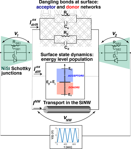
Figure 4. Equivalent circuit representing the multiple transport mechanisms in SiNW.
Download figure:
Standard image High-resolution imageThe fabricated structures are characterized by a p-doped nanoscale channel (35 nm) with surface roughness and defects. Surface defects can give rise to energetically active surface states continuously distributed in energy within the silicon band-gap [3, 33, 34]. Their charge state is Fermi-level dependent [35], thus defining the amphoteric nature of the surface traps. Depending on the position of the semiconductor Fermi level with respect to the charge neutrality level (namely the level at which surface charges are compensated by the bulk doping atoms), the surface states can act either as electron acceptors or electron donors, being associated with either acceptor-like or donor-like energy levels, respectively [36]. Figure 5 illustrates a possible schematic model of the surface of a SiNW with native oxide and surface trap centers, where surface state recombination occurs due to the adsorption of external molecules such as ABs.

Figure 5. Sketch of the formation/recombination of energetic surface levels. Neutral (black spheres), acceptor-like (blues spheres) and donor-like (red spheres) states are from surface defects. Charging phenomena at the surface take place via binding of charged species such as ABs.
Download figure:
Standard image High-resolution imageAll the transport mechanisms we deal with at the surface can be subdivided into drift and diffusion components [37–39]. We describe in detail each of them separately.
Current components from surface states. In the most simplified approximation, the drift component of donor-like and acceptor-like surface trap centers can be described by resistor–capacitor (RC) networks [39] acting independently when a voltage is applied across them (figure 4). The overall effect arising from the activity at the acceptor (donor) sites is reduced to an equivalent resistance Ra (Rd) in parallel to an equivalent capacitance Ca (Cd). In first approximation, and for short wires, the electrical capacitances of acceptor and donor RC networks can be assumed proportional to the number of acceptor, na, and donor, nd charges, respectively, because they act as parallel capacitances associated with their respective charges. If na(t), nd(t) and nn(t) denote the time dependent amount of acceptor-like (negatively charged), donor-like (positively charged) and neutral traps, respectively, the total number of charge states N0 can be expressed as:

Therefore, the various capacitances can be defined as:

where  (acceptor, donor),
  is the overall capacitance of the trap systems, and the initial condition for the nα are discussed in section III of the SI. The equivalent resistances of surface charged centers, Rα, with
  can be estimated by means of the Einstein relation [40], and expressed as:
where q is the electric charge of a particle,  stands for the electrical mobilities of the charged traps, A is the transport area, kB is the Boltzmann constant, T the absolute temperature, and
  the free energy change for surface traps to vary their states [40].
Using relations (2) and (3) the drift surface current Ioxdrift, driven by the external voltage bias V(t), and due to the impedance of the RC network, is created by the hopping of charges from one surface trap to another and reads:

where VNW is the voltage drop across the nanowire channel (see figure 4).
The second contribution to the surface current is given by the diffusion current Ioxdiff. The diffusion process is due to the concentration gradient of charged surface states. From the current continuity equation, following the approximation described in [39], and also discussed in section II of the SI, we have

where fa and fd are self-similarity parameters (see SI for the definition) to be fitted to the experimental data, and e the electron charge.
Assuming that no mixing of acceptor-like and donor-like states occurs at low frequency we can approximate the recombination/formation rate of the surface traps na(t) and nd(t) as a linear function of the surface state densities:

where  , and kdd, kaa and
  denote the charge acceptor, donor and neutral rate constants, respectively. The first term on the r.h.s. of equation (6) represents the inter-band hopping of charge species α from its band to the neutral band (state recombination), while the second term represents the reverse process (state formation). These rate constants are estimated using the modified Arrhenius rate equations [39]:

with  ,
,  and
and  ,
,  the rate constants of acceptor and donor traps in their charged or neutral state, respectively, applicable when
  . Moreover,
  is not independent among them and its dependence is discussed in section III of the SI.
  is the average energy for the inter-band formation/recombination processes (see SI for the continuum to discrete energy band approximation).
  and
and  represent the symmetrization factors; σ describes the response of the rate constants to the external voltage due to multiple scatterings.
Current components from the SiNW bulk. The electronic transport in the bulk of the SiNW is described by drift INWdrift and diffusion INWdiff components. INWdrift can be expressed as a function of the wire resistance RSi and voltage drop VNW across it:

where RSi is estimated as  , with
  the resistivity of low (
 ) boron doped silicon (5M
  ), and L and A the length and the cross section area of the wire, respectively.
The diffusion component INWdiff depends on the concentration gradient of the net charge into the nanowire. In this case, we can estimate the total net charge in the bulk as the sum of the net charges Q1 and Q2 at the depletion regions induced by the Schottky contacts. Using again the approximation in section III of the SI, the diffusion current in the wire can be thus estimated as:

with fs a self-similarity coefficient resulting from the continuity equation approximation (see section II of the SI). The net charges Q1 and Q2 can be evaluated using the standard expression for depletion region net charge [37]  where j = 1, 2, S is the section area of the junctions and Nd the number of ionized donors of the p-type SiNW. wd1 and wd2 are the thicknesses of the left and right depletion regions formed by the Schottky junctions at the source and drain terminals and can be estimated as [37]
  with
with  the built-in potential of the NiSi/Si junction, and V1 and V2 the voltage across the left and right Schottky barriers, respectively.
Current components from the Schottky contact. The last factor affecting the electrical behavior of the voltage gap based sensor is the metal–semiconductor interface. The NiSi Schottky barriers can be modeled as different elements in parallel (figure 4): the resistance RSB1 (RSB2), capacitance CSB1 (CSB2), and the diode D1 (D2) define the left (right) NiSi Schottky barrier of the nanowire. From the equivalent circuit, it derives that the current flowing through the left and right Schottky barriers is expressed as:
with j = 1, 2. IS1 and IS2 are the saturation currents of the left and right diodes and are defined by [38] ![${I}_{{\rm{S}}{j}}={A}^{* * }{T}^{2}S\mathrm{exp}[-q{\phi }_{{\rm{b}}{i}}/{k}_{{\rm{B}}}T]$](https://content.cld.iop.org/journals/0957-4484/27/34/345503/revision1/nanoaa2c44ieqn25.gif) with
with  the Richardson's constant and
  the built-in potential of the NiSi/Si junction. The resistances of the Schottky diodes RSB1 and RSB2 can be estimated by the contact-resistance relationship [37]
 ![${R}_{{\rm{c}}}=\tfrac{{k}_{{\rm{B}}}}{{A}^{* * }{Tq}}{{\rm{e}}}^{[q{\phi }_{{\rm{b}}{i}}/{k}_{{\rm{B}}}T]}$](https://content.cld.iop.org/journals/0957-4484/27/34/345503/revision1/nanoaa2c44ieqn28.gif) . The Schottky diode capacitances CSB1 and CSB2 are expressed by the diode capacitance–voltage relationship [41]
. The Schottky diode capacitances CSB1 and CSB2 are expressed by the diode capacitance–voltage relationship [41]  , where Cj0 is the zero-bias junction capacitance and γ is a parameter representing the doping profile of the active junction layer (
 for a uniformly doped junction layer). The zero-bias junction capacitance is
  with
with  and
and  the vacuum dielectric constant and the relative permittivity of the silicon, respectively.
Dopant atoms introduced into semiconductors are known to have the effect of varying the effective barrier height in a given metal–semiconductor contact [37, 38]. Surface charges have a similar effect on the junctions of our device and induce a Schottky barrier lowering  . The image-force lowering, also known as the Schottky effect or Schottky barrier lowering, is the image-force-induced lowering of the barrier energy for charge carrier emission, in the presence of an electric field. The charge carriers in our case are represented by the charges related to the surface distribution of acceptor and donor trap states. The barrier lowering is estimated by considering the image-force lowering theory [37]
  where ns is the charge volume density given by the sum of the net surface charge volume density
  , the bulk doping atoms Nd, and
  the surface potential. The barrier lowering affects the Schottky barriers by changing the saturation currents with two terms related to the different effects of positive (donors) and negative (acceptors) mobile charge carriers at the Schottky barriers: positive carriers see a barrier height
  , while negative carriers see a barrier
  where
where  is the silicon energy band-gap:

4. Results and discussion
By combining all the analytical formulations reported in the previous section, the circuit of figure 4 can be solved for a varying external voltage. The phenomena at the SiNW surface, in the bulk, and at the Schottky barriers can be expressed by a system of differential equations in the four variables  ,
,  , na(t) and nd(t). This system describes the dynamic interaction of the nanodevice with the incoming molecules, and its solution defines the current–voltage relation, enabling the comparison with the electrical characteristics acquired during the experiments. The analytical formulation of the circuit was implemented in Matlab, and the solution was calculated throughout an implicit numerical solver endowed with time step size control programmed ad hoc for this particular problem.
The external bias voltage is swept from −2.5 to +2.5 V and, in accordance with the experimental measurements, varies as a piecewise increasing and decreasing linear function with a slope of ±50 mV s−1. The current in the Ids–Vds characteristic is given by the concurrent contributions of drift and diffusion components both in the surface native oxide ( ) and in the bulk of the nanowire (
 ), and of the effects at the junctions (
 ). The implementation of the system required the estimations of different physical parameters for modeling the different components of the current, as well as the fitting of some of them to the experimental data.
First, we considered the case of bare nanodevices, and we compared a real Ids–Vds measurement acquired from a SiNW after the fabrication and before any modification with biological material (figure 6(a)) with a simulated characteristic (figure 6(b)). As clearly evident from the plots, the simulated curve fits well the experimental one and models pinched hysteretic behavior (figure 6(b)). Figure 6(c) illustrates the corresponding components of the total current calculated in the simulation, components that are strictly dependent on each other and that affect the total current with their continuous competition/compensation. In the diagram, both forward and backward branches of the current are shown in order to better demonstrate the similarities between the experimental and modeled curves under external voltage sweep.
Figure 6. Experimental (a) and simulated (b) Ids–Vds characteristics of a SiNW before any surface biomodification. Both curves have pinched hysteresis loops, similar to the hysteresis of memristive-like behavior, and same current peak. Blue and red curves denote the forward and backward current branches, respectively. (c) Corresponding components of the total current reported in (b). The parameters chosen for this simulation are:  Hz,
Hz, 
![$=\;{k}_{{\rm{a}}0}^{{\rm{a}}}/[8.4({N}_{0}-{n}_{{\rm{d}},0})/{n}_{{\rm{d}},0}]$](https://content.cld.iop.org/journals/0957-4484/27/34/345503/revision1/nanoaa2c44ieqn48.gif) ,
,  Hz,
Hz,  ,
,  F,
F,  MΩ,
MΩ,  MΩ,
MΩ,  ,
,  ,
,  ,
,  ,
,  ,
,  ,
,  ,
,  .
.
Download figure:
Standard image High-resolution imageThe current  arises from the dynamic exchange of charges at the surface trap states. The drift current in the surface oxide depends on the capacitances and resistances of the surface states in the oxide.
  and
and  affect the total current because their product is comparable to the time of the system. Their effect varies as a function of the charge density
  as a result of their definition (equations (2) and (3)).
Considering that the mobility of negative carriers, related to the acceptor states, is much higher than the one of positive carriers from donor centers ( cm2 V−1 s−1,
  cm2 V−1 s−1 in p-doped silicon [42–44]), we observe that only the acceptor component contributes to the drift transport being
  MΩ, much smaller than
  MΩ as estimated by equation (3). However, because of the high resistances of the surface trap networks in bare condition, the diffusion Ioxdiff related to the occupation of the acceptor and donor energy levels dominates (over Ioxdrift) the electrical transport at the surface (figure 6(c)).
The energy level related to the negatively charged acceptor states na is estimated [35] to be  , while the one corresponding to the positively charged donor states nd is estimated [35] to be
  . Consequently, the threshold energy associated with the neutral state is
  for acceptors and
  for donors, respectively, Ei being the intrinsic energy level of the semiconductor. The terms fa and fd in equation (5) are fitted to the experiments via Monte-Carlo simulations. Both in the bare and biomodified case they appear to be large (
 ,
,  in the simulation curve of figure 6(b)). This indicates very small variation between the incoming and outgoing diffusion currents through the left and right surfaces of the SiNW, respectively (see section III of the SI). The diffusion current is plotted with solid curve in figure 6(c), and, as clearly visible in the figure, by looking at the amplitude of this component compared to the total curve of figure 6(b), it has the most important role in defining the pinched hysteresis loop in bare nanowires.
A further contribution may also come from the electronic transport in the bulk of the SiNW. However, both drift and diffusion currents in the nanowire core seem to be negligible in the condition in which external charged molecules are absent. INWdrift is not reported in figure 6(c) because of its very low amplitude. The low current values result from the fact that the nanowire channel can be approximated with a fully depleted channel as a consequence of the NiSi Schottky barriers, at both ends, defining depletion regions with thickness  . The depletion in the channel increases the resistance RSi and makes the drift current of the bulk INWdrift negligible. Therefore, most of the current contributing to the transport in the SiNW core is given by the diffusion of carriers in the depleted regions (dotted curve in figure 6(c)).
The conductivity both in the nanowire and in the oxide is finally affected by the Schottky barriers (equation (10)), whose height has been estimated to be  [45]. No or little barrier lowering occurs in the absence of biomolecules. The junctions determine a small voltage drop at the NW contacts that limits the amplitude of the Ids–Vds characteristics of the device if compared to the biomodified condition that will be discussed in the following (figure 7). Most importantly, the condition of zero, or very small voltage gap, is directly related to the null quantity of acceptor states na and the low number of positively charged donor states nd with respect to the total number of surface defects N0 onto the native oxide. This value (
 ) demonstrates the balance of charges at the surface of the nanowire (neutral surface states) and the existence of few charged donor states mostly deriving from the doping atoms in the p-type semiconductor.
Figure 7. Modeling the voltage gap. (a) Semi-logarithmic Ids–Vds characteristic from experimental measurements acquired from a fabricated SiNW functionalized with ABs. The voltage gap appears as a result of the adsorption of positively charged species onto the nanowire and the interaction with the oxide surface states. (b) Simulated total Ids–Vds curve. (c) Components of the characteristic reported in panel (b): diffusion current due to the surface states in the oxide (solid curve); drift current in the oxide (dashed curve); diffusion current in the SiNW (dotted curve). (d) Individual contributions of acceptor (solid curve), and donor (dashed curve) states to the diffusive current at the NW surface. The parameters chosen for this simulation are:  Hz,
Hz, ![${k}_{{\rm{n}}0}^{{\rm{a}}}={k}_{{\rm{a}}0}^{{\rm{a}}}/[14({N}_{0}-{{\rm{n}}}_{{\rm{d}},0})/{{\rm{n}}}_{{\rm{d}},0}]$](https://content.cld.iop.org/journals/0957-4484/27/34/345503/revision1/nanoaa2c44ieqn80.gif) ,
,  ,
,  ,
,  F,
F,  ,
,  ,
,  ,
,  ,
,  ,
,  ,
,  ,
,  .
.
Download figure:
Standard image High-resolution imageFigure 7 shows the nanowire behavior once exposed to charged molecules. Again, both forward and backward sweeps are highlighted. In figure 7(a), the Ids–Vds curve acquired from one memristive biosensor, i.e. a SiNW functionalized with ABs, which are positively charged species at physiological pH [46], are plotted. The biomodification determines the increase of the current maxima (two orders of magnitude bigger than the bare case (figure 6)) and, most relevantly, the appearance of a voltage gap defined by the different values acquired by forward and backward curves for the zero-current condition. Figure 7(b) is the plot of the simulated Ids–Vds curve.
Similar to the experimental curve, simulations show an increased current peak ( A) and a voltage gap of
  . The total simulated current in the SiNW is given by the sum of the different contributions (figure 7(c)) arising from the drift (dashed curve) and diffusion (dotted curve) current in the surface state network, and the diffusion in the nanowire channel (dotted curve), and is also dependent on the effects at the junctions. In addition, in this case, INWdrift can be neglected because of the fully depleted wire. As shown in figure 7(c), the predominant effect is given by the dynamic surface exchange of the energy levels, i.e. the diffusion in the oxide. This component is the result of the competing action of donor and acceptor states described by
  and
and  , respectively, in figure 7(d). The two currents depend on the constant rates
  and
and  whose values were of the same order of magnitude in the case of pinched-loop hysteresis, i.e. bare devices (
 Hz), but now differ by three to four orders of magnitude, one with respect to the other. In particular, the dynamics of the energetic donor levels has increased (
 Hz), thus demonstrating that biomolecules attached to the nanowire surface favor the occupation of the donor energy levels. This occurs in combination with the increased number of positively charged donor levels nd. This can be physically explained by considering the approaching and the binding of positively charged biomolecules, the ABs, to the surface of the nanowires. In other words, the incoming proteins charge the surface by providing positive charges and determine the occupation of the energetic levels associated with the donor defects. Negatively charged na do not interact with the external positive charges and cannot compensate for them, because of their null density at zero bias and in the initial condition of bare surfaces. However, with the adsorption of ABs, the formed biolayer may lead to the creation of new surface defects. These surface defects can be associated with acceptor energy levels, thus explaining the slowly increasing dynamics exchange for the acceptor-like surface states (
 ). This is also confirmed by the increase of total number of surface traps N0 in the curve simulating the voltage gap change after biofunctionalization (
 ).
).
The surface trap capacitances  and
and  increase by two/three orders of magnitude with respect to the simulation of figure 6(b), due to the accumulation of a biolayer onto the device surface. However, these capacitances still do not affect in a relevant way the drift current in the oxide because of the low frequency of the biasing signal (order of mHz).
Thanks to its high dependence on external charges coming from the surrounding environment, the voltage gap can be used as biosensing parameter. The application proposed in this paper is the detection of AG molecules in a very challenging environment, which is a breast TE (figure 3(c)). As briefly explained above, the biosensing is determined by the electrical measurement of the voltage gap decrease from nanowire, which has been previously functionalized with ABs, namely the memristive biosensors, and successively exposed to increasing concentrations of target species. According to the theory proposed in this paper, the reduction of the voltage gap in the Ids–Vds characteristics is related to the charge compensation at the surface of the wire, where surface defects can easily become sites of charge accumulation under external sweeping bias and exposure to proteins. In figure 8 we demonstrate that our theory can model this dependence of the voltage gap on the increasing concentration of AGs, by correlating it to the formation and recombination of the charged surface states in the oxide of the SiNW.
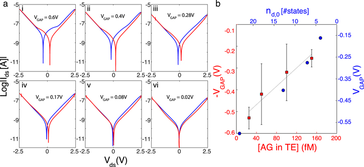
Figure 8. (a) Simulated Ids–Vds characteristics modeling the increasing uptake of AG molecules onto a biomodified nanowire. The parameters chosen in these simulations are:  ,
,  ,
,  F,
F,  ,
,  ,
,  ,
,  . Only some of the parameters in the model vary affecting the hysteresis and the voltage gap, demonstrating the importance of the charge imbalance induced by the dynamic modification of the surface states. Moving from plot (i) to plot (vi),
  decreases from 0.5 to 0.07, N0 decreases from 47 to 8.4, and the donor rate constant
  decreases exponentially from
  (i) to four orders of magnitude smaller in case (vi). (b) Reports the variation of the voltage gap as a function of
  (blue axes) and compares it to the calibration data from experiments (figure 3(b)) in a breast TE (red axes). As the AG concentration increases the positively charged surface states decrease due to charge compensation, thus determining a reduction of the voltage gap.
Download figure:
Standard image High-resolution image
The subplots in figure 8(a) give, from left to right and from top to bottom, simulated semi-logarithmic curves modeling the fabricated biosensor from the case of zero AG to the one of uptake of increasing concentrations. According to the surface trap mediated theory, the reduction of the voltage gap, combined with the lowering of the current peak, occurs as a result of different varying factors that have been observed from the simulation of the system. In general, they are related to variation in the surface states and their dynamics. Considering a linear variation of the AG concentration from the case of figure 7, where the NW only carries positively charged ABs on its surface (0 fM) to the extreme case of AG concentrations saturating the sensor and determining a reduction of the voltage gap (figure 8(a), case (vi)) back to the starting pinched hysteresis loop (figure 6), the parameter  decreases from 0.5 to 0.07, the parameter N0 decreases from 47 to 8.4, and the donor rate constant
  decreases exponentially from
  (i) to four orders of magnitude smaller in case (vi). The variation of the voltage gap as a function of
  is reported in figure 8(b) (blue axes) and superimposed to the experimental data (red axes) of figure 3(c) for comparison. This diagram demonstrates that the simulated results describe well the registered behavior of the voltage gap in real experiments of AG sensing in breast TEs, the first time reported for memristive biosensors, and explains the relationship between the sensing parameter and the decreasing number of positive surface states (
 ) on the wire as effects of increased concentration of AG and the occurrence of AB/AG binding phenomena resulting in charge compensation.
5. Conclusions
In conclusion, we have shown that the voltage gap sensing phenomenon in memristive biosensors is modeled by several combined effects of charge transport occurring at the nanowire surface; inside the wire and at the NiSi junctions. Despite the single phenomenon occurring in the sensor being relevant to the determination of the memristive behavior of the device, and its modification in terms of voltage gap appearance, the major contribution comes from the dynamic occupations of the nanowire surface state energy bands, enabled by the incoming external charges from bio-species. This shows the importance of surface electrical transport in the oxide of the functionalized device.
We have presented the implementation of an analytical model able to reproduce and explain the voltage gap based behavior in NiSi Schottky barrier memristive biosensors, which successfully accounts for the detection of different concentrations of biomarkers for breast tumor screening. Moreover, the developed theory enables the capture of the dynamics of the voltage gap by using only a small set of parameters that are linked to the concentrations of antigens, thus enabling a determination of the number of antigens. Taking into account the direct correlation with the physics of the nanodevice, and the compactness of the model, our theory can be also used to model and predict the voltage gap based behavior in other similar nanostructured devices and sensors. This may be useful for several different applications ranging from biological and chemical sensing to electronics.
Acknowledgments
FP and SC acknowledge support from Swiss SNF CoRE project CR32I3/156915/1. FLT and MD acknowledge support from DOE under Grant No. DE-FG02-05ER46204. GD acknowledges support from H2020-ERC 2014-ADG–669354: CyberCare.