

Abstract
Perpendicular magnetic tunnel junctions (p-MTJs) were patterned into nanopillars using electron-beam lithography to study their scaling and switching behaviour. Magnetoresistance measurements of annealed and unannealed p-MTJ films using scanning probe microscopy showed good agreement with Monte Carlo modeling. p-MTJ pillars demonstrated clear parallel magnetic states, both 'up' or both 'down' following AC-demagnetization. Significant variability in the resistance of p-MTJ pillars was observed and attributed to edge features generated during patterning or local inhomogeneity in the MgO layer.
Export citation and abstract BibTeX RIS
1. Introduction
Magnetic tunnel junctions with easy axis perpendicular to the film plane (p-MTJs) have been extensively studied in the last 10 years. [1, 2] They have great potential as a building block in non-volatile spintronics such as spin-transfer-torque magnetic random access memories [3, 4] because p-MTJs in general require lower critical switching currents than devices with in-plane anisotropy. In p-MTJs the perpendicular magnetic anisotropy (PMA) originates from the interfacial anisotropy at the CoFeB/MgO interface, and the anisotropy is sufficient to produce magnetic stability even for dimensions below 20 nm. However a number of technological challenges must be met before magnetic random access memory based on spin transfer torque effect (STT-MRAM) and related devices can be widely implemented [4, 5] particularly at sub-50 nm dimensions. These issues include the cell to cell variability and the tunnel magnetoresistance (TMR) amplitude and temperature stability, as well as circuit designs and architectures.
Cell variability originates from edge defects generated during patterning of the cells, and damage to the MgO layer yields local changes in the barrier resistance, TMR and magnetic anisotropy, affecting data retention [3]. A metric of the variability is the switching field distribution of arrays of p-MTJ nanopillars and how this changes with processing methods and as the pillar dimension is reduced.
In this work, the scaling and switching behaviour of p-MTJ pillars with a structure of Ta/CoFeB/MgO/CoFeB/Ta and Mo/CoFeB/MgO/CoFeB/Mo were studied for pillars diameters down to 45 nm. A fabrication method was developed, which enables patterning of p-MTJ pillars while preserving the magnetic quality of the layers. Annealing increased the TMR of the patterned p-MTJ pillars and sharpened the switching of both magnetic layers. Experimental results for the hysteresis loops of annealed and unannealed pillars are in good agreement with the results of Monte-Carlo (MC) modeling. We also demonstrated that after AC-demagnetization the p-MTJ pillars support two possible single-domain states with the magnetization of the magnetic layers oriented parallel, both 'up' or both 'down', but the resistance shows variability between different pillars.
2. Methods
Films with a structure of Si/SiO2/Ta(6 nm)/Ru(10 nm)/Ta or Mo(10 nm)/Co20Fe60B20(0.8 nm)/MgO (1–3 nm)/Co20Fe60B20(1.5 nm)/Ta or Mo(7 nm)/Ru(8 nm), schematically represented in figure 1((a) were deposited in a multisource ultrahigh vacuum magnetron sputtering system with a base pressure of 3 × 10⁻⁹ Torr. The Co20Fe60B20 composition represents atomic percent. The key layers in the stack are the CoFeB/MgO/CoFeB tunnel junction, in which the MgO film formed a wedge across the sample of varying thickness, and the other layers provide seed and capping layers.

Figure 1. (a) A schematic of the magnetic tunnel junction multilayer used in this work. (b) Tunnel magnetoresistance versus magnetic field for unpatterned Mo/CoFeB/MgO/CoFeB/Mo- and Ta/CoFeB/MgO/CoFeB/Ta-based magnetic tunnel junctions of 25 μm diameter and 10 mV bias voltage.
Download figure:
Standard image High-resolution imageAfter deposition, the unpatterned p-MTJ films were annealed at 300 °C for 10 min in a rapid thermal annealing system in a pure Ar atmosphere. Thermal annealing is a crucial step in achieving high TMR ratios [6–8] by establishing PMA in both layers. The anneal had to be performed before patterning, because post-annealing the p-MTJ devices degraded their hysteresis, attributed to oxidation at the edges of the features. Both TMR and PMA had a strong dependence on annealing time. The TMR ratio reached 120% for unpatterned films of CoFeB/MgO/CoFeB with the Mo layer and 100% for the sample with the Ta layer. The TMR versus magnetic field curves for the Ta/CoFeB/MgO/CoFeB/Ta and Mo/CoFeB/MgO/CoFeB/Mo films at room temperature are presented in figure 1(b). The low- and high-resistance states represent parallel and antiparallel magnetization, respectively, of the two CoFeB layers from which the switching fields of the unpatterned layers can be measured. The bottom, thinner CoFeB layer switches at a higher magnetic field and more sharply than the top layer [9], as a result of its higher anisotropy.
The annealed p-MTJ multilayers were patterned using electron-beam lithography (EBL) and ion beam etching to create circular pillars in a process shown in figure 2. Features of 13 nm diameter and above were achieved in hydrogen silsesquioxane (HSQ) resist with a Elionix 125 EBL tool. HSQ 2% solution (XR-1541-002, Dow Corning) was spin-coated and exposed at 10 kV acceleration voltage with a 120 μm aperture, resulting in a beam current of 500 pA–2 nA. Circular structures were exposed as single-pixel dots using a dose of 2 × 10⁶ μC cm−2. The samples were then developed in aqueous 1 wt% NaOH, 4 wt% NaCl in de-ionized (DI) water each for 4 min at 24 °C developer temperature, followed by rinsing with DI water for 2 min and drying in a N2 stream. Development was done by sample immersion without agitation in a beaker containing the developer solution. It is important to ensure that the rinse in DI water was long enough (2 min) to completely avoid any deposition of NaCl salt crystals on the surface of the substrate [10]. The sizes of the patterned HSQ patterns were measured via scanning electron microscopy (SEM). The exposed and developed pattern consisted of circular HSQ pillars of different sizes, shown in figure 3(a).

Figure 2. Schematic of the sequence of fabrication steps used for making p-MTJ pillars. (a) Resist spinning end exposure. (b) Development. (c) Ion beam etching. (d) Removal of HSQ. Layer thicknesses are not to scale.
Download figure:
Standard image High-resolution image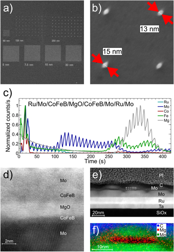
Figure 3. (a) and (b) SEM micrographs of HSQ pillars on a continuous CoFeB/MgO p-MTJ patterned at 10 kV acceleration voltage in a Elionix 125 EBL system and developed using a salty developer. (c) Etch profile of the Mo/CoFeB/MgO/CoFeB/Mo MTJ. (d) ABF-STEM image of pMTJ pillar with Mo/CoFeB/MgO/CoFeB/Mo structure. (e) HAADF-STEM image. Dotted outline shows the pMTJ. (f) EELS image with overlay of C-K1, Mo-M2,3 and Mg-L1 signals. C is plotted in blue, Mg in red and Mo in green.
Download figure:
Standard image High-resolution imageIn the next step, ion beam etching (ion milling) was used to transfer the pattern into the p-MTJ down to the bottom conductive Ru layer using Ar ions at base pressure 1 × 10⁻⁷ Torr, with Ar flow of 1.5 sccm, 8 mA beam current, and a 2 cm beam diameter, schematically shown in figure 2(c). In order to control the etching process a Hiden end point detector was used. An example of an ion beam etch profile from the end-point detector is given in figure 3(b) for a Si/SiO2/Ta(6 nm)/Ru(10 nm)/Ta(10 nm)/Co20Fe60B20(0.8 nm)/MgO(1–3 nm)/Co20Fe60B20(1.5 nm)/Ta(7 nm)/Ru(8 nm) p-MTJ. The signals from various elements can be resolved as a function of time, making it possible to stop at the bottom conductive Ru layer. The periodic variations are due to the sample rotation during the etching process. The residual HSQ mask material was removed with a reactive ion etch using CF4 (figure 2(d)). The top Ru layer provided a conductive contact for conductive atomic force microscopy (cAFM) measurements.
Figure 3(a) lower panels show scanning electron micrographs of HSQ pillars imaged at 3 kV using a Zeiss Merlin high-resolution scanning electron microscope. The best patterning resolution on the Elionix EBL tool resulted in 13 nm diameter structures in HSQ but the pattern transfer process broadened the features to around 40 nm diameter measured by SEM. The largest features made here were 2 μm diameter.
Conductive AFM measurements were done using a RHK UHV350 with R9 controller in contact mode and an Asylum Research Cypher AFM tool. Conductive probes were fabricated by coating commercial non-conducting probes with nominally 200 nm of Pt on a Ti adhesion layer using a process detailed elsewhere [11, 12]. Commercial conductive probes, Rocky Mountain Nanotechnology RMN 12Pt300B, were also used. The conductive AFM measurements were made in ambient atmosphere at room temperature. A magnetic field between ±500 Oe perpendicular to the sample was applied using an electromagnet below the sample. Maps of the topography and current were obtained by scanning the AFM probe over a 2 μm × 2 μm region to locate the patterned nanopillars. The probe was then moved onto individual nanopillars to perform transport measurements in constant force mode at a fixed location. Resistance as a function of magnetic field was recorded by holding the sample at a fixed voltage relative to the grounded tip and recording the current while sweeping the magnetic field at a rate of 345 Oe/s. Sample biases of 100, 600, and 900 mV were used. Measurements were repeated multiple times for each bias and multiple devices of each size were measured. The magnetic properties of the pillar arrays and continuous films were determined using magnetic force microscopy (MFM) Cypher AFM and of the continuous films by vibrating sample magnetometry using a microsense VSM.
Since it would be quite difficult to locate and align the p-MTJ pillars on the EBL-patterned sample in the scanning transmission electron microscope (STEM) we collected the STEM images from samples which were patterned using block copolymer lithography. The patterning was done by covering the p-MTJ stack with 20 nm sputtered carbon, then a film of polystyrene-b-polydimethylsiloxane block copolymer, which was annealed to form a close-packed sphere array. The pattern was transfered to the carbon by oxygen etching, then to the p-MTJ film by using ion beam etching, which produces a dense array of p-MTJ pillars of center to center spacing about 40 nm, based on SEM images. The cross-sectional STEM and spectrum image of a p-MTJ with MgO thickness of 1–3 nm are shown in figures 3(d) and (e). STEM samples were prepared by the focused ion beam lift-out method after coating with protective Pt layer. The acceleration voltage was reduced to 2 kV at the end to reduce damage. To avoid contamination during imaging the samples, before going into the microscope the sample was plasma-cleaned for 5 min with 25% O2 in Ar at 22 psi with a plasma cleaner (Fischione model 9020). STEM and electron energy loss spectroscopy (EELS) images were acquired in a FEI Titan STEM with a probe aberration corrector operated at 200 kV.
Figures 3(d) and (e) show STEM image of a p-MTJ pillar with the Mo(10 nm)/CoFeB(0.8 nm)/MgO(1–3 nm)/CoFeB(1.5 nm)/Mo(7 nm) structure. Figure 3(e) is a medium magnification high angle annular dark field (HAADF) STEM image. The HAADF image intensity scales as Zα, where α is in the range of 1.6–1.9 and Z is the atomic number. This Z-contrast effect was used to distinguish the different layers of the pillar. HAADF STEM images were collected with a 24.5 mrad probe semiangle, STEM resolution of 0.8 Å, and HAADF detector range of 54–270 mrad. We checked over 100 p-MTJ pillars and found that in pillars with resolved CoFeB/MgO/CoFeB, MgO was polycrystalline. The dark area on figure 3(e) corresponds to the active part of the p-MTJ, namely CoFeB/MgO/CoFeB. This can be seen from figure 3(d), which is a high magnification annular bright field (ABF) STEM image with ABF detector angle from 5.7–12.6 mrad. Weak contrast of the CoFeB layers is due to interface roughness.
Figure 3(f) shows a typical spectrum image measurement of the diameter of Mo/CoFeB/MgO/CoFeB/Mo p-MTJ pillar. Electron energy loss signals of boron and cobalt were too weak to map. From such images we can estimate the length of the active part of the p-MTJ pillar, which is typically 17–18 nm, smaller than the nominal pillar diameter from SEM images. Although the lithography process is different from that of the EBL samples, the ion beam etching step was the same and we expect the edge profile of the dots to be representative of that of the EBL-patterned samples.
3. Results and discussion
3.1. cAFM of CoFeB/MgO p-MTJ pillars
Figures 4(a) and (b) demonstrate typical TMR major and minor loops of annealed CoFeB/MgO pillars of 60, 125 and 250 nm diameter recorded at +900 mV sample bias. Minor loops were recorded by initializing the p-MTJs into the low resistance state with a positive perpendicular field and then sweeping the field without reversing the magnetization of the thin (hard) CoFeB layer. The two magnetic layers in the p-MTJ nanopillars had well-separated and sharp switching fields. The coercivity of the CoFeB layers in perpendicular MTJs is inversely related to the CoFeB thickness [9, 12, 13]. The TMR was in the range of 20%, consistent with [12], which shows that TMR decreased with increasing sample bias, from approximately 100% at low bias to just below 20% at 900 mV bias.
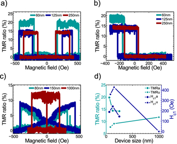
Figure 4. Field-induced switching of individual pillars: (a) major TMR loops and (b) corresponding minor TMR loops of annealed p-MTJ CoFeB/MgO pillars of 60, 125 and 250 nm recorded at 900 mV sample bias; (c) major TMR loops of unannealed p-MTJ CoFeB/MgO pillars of 80, 150 nm and 1 μm. (d) TMR ratio and hard layer switching field Hc1 as a function of the pillar diameter for annealed (subscript a) and unannealed (u) samples.
Download figure:
Standard image High-resolution imageThe switching fields of the two layers, denoted as Hc1 for the hard layer and Hc2 for the soft layer, both of which generally increased with decreasing pillar diameter, can be measured from the major loops. The switching fields in the major loop include the effect of magnetostatic interactions between the two layers. The offset to the minor loop allows the stray field  of the hard layer acting on the soft layer to be determined, as well as the coercivity of the soft layer
  from the half-width of the minor loop. The minor loops give
  = 160, 65 and 45 Oe and
  = 10, 95 and 95 Oe for diameters of 60, 125 and 250 nm respectively. The bottom harder CoFeB layer magnetization can only be reversed in a major loop [12] so the effect of the soft layer field on the hard layer cannot be determined from Hc1. Smaller devices, 45 nm diameter, showed a resistance that was consistent with their area but the 600 Oe field available from the magnet in the cAFM was insufficient to switch both magnetic layers.
In contrast, figure 4(c) shows TMR major loops of CoFeB/MgO pillars of 80, 150 nm and 1 μm diameter made from an unannealed film, recorded at sample bias between 100 and 400 mV. The largest device showed sharp switching, but the 80 and 150 nm pillars demonstrate butterfly shaped hysteresis. The loop shapes originate from in-plane anisotropy in one CoFeB layer and will be discussed in more detail in the next section. The TMR is slightly smaller than that of the annealed samples despite the lower bias voltage. Figure 4(d) summarizes the TMR and hard layer switching field Hc1 versus pillar diameter, with subscripts a and u representing annealed and unannealed samples respectively. Finally, the product of resistance and area (RA product) was measured for both the annealed and unannealed MTJs, and was unaffected by area for diameters down to 80 nm. The RA product depends sensitively on the MgO thickness so its value was a function of position along the sample.
3.2. MC modelling of TMR in p-MTJ pillars
A MC model was used to qualitatively illustrate the hysteresis loops and the TMR of pillars consisting of two magnetostatically interacting layers of different anisotropy. MC considers dipolar, anisotropy and Zeeman energy terms and includes the effects of temperature, external magnetic field and relative anisotropies of the ferromagnetic layers. The magnetoresistance is determined from the relative orientation of the magnetic moments of the two CoFeB layers [14, 15], by calculating the thermal average of the angle between all pairs of adjacent magnetic moments in the two layers.
In the experiment the CoFeB layers have cylindrical shapes with a radius of about 100 nm and a height of 1–2 nm. Nanostructures of this geometry are expected to reverse incoherently, but for simplicity we treat the magnetic CoFeB layers as macrospins. The system then consists of two effective magnetic moments,  and
and  . Each layer is characterized by a uniaxial easy axis
  and an anisotropy constant
  where
where  , with
  the volume,
  the magnetization and
  the anisotropy field. The energy E of the system under an external magnetic field
  is given by
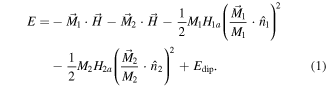
Here Edip is the dipolar interaction between the two magnetic moments separated by a distance r12 (the thickness of the MgO layer).  is a unit vector pointing in the direction from magnetic moment 1 to 2, or vice versa. Edip is given by

We performed MC simulations at room temperature (T = 300 K) using the expression for E as a function of an external magnetic field, from −1 kOe to 1 kOe. The parameters were chosen to produce switching of the magnetic layers whithin this field range. A magnetization value of 1300 emu cm−3 was used. An anisotropy value of about  was taken for the soft layer correspondng to an anisotropy field of 300 Oe. The relative anisotropies of the layers was parameterized by the ratio
  which gives the ratio of anisotropy energies between layers 1 and 2.
Figures 5(a) and (b) demonstrate plots of hysteresis loops and magnetoresistance as a function of external magnetic field H for the system CoFeB-1.6 nm/MgO-1.0 nm/CoFeB-0.8 nm, when both layers have PMA. The results are shown for anisotropy energy ratio r = 0.2 or 0.5. For H = 0, the CoFeB layers have parallel magnetization and the resistance R is low, but an increasing field reversed the softer CoFeB layer giving an antiparallel state corresponding to the high resistance plateau. Higher r gave a larger switching field for both layers, and the field range for the plateau was smaller. Notably the switching fields in the ascending and descending branches of the loops are not necessarily symmetrical, which reflects the finite temperature of the model leading to stochastic switching.
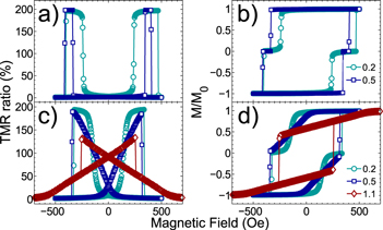
Figure 5. Hysteresis loops and magnetoresistance of CoFeB/MgO/CoFeB p-MTJs calculated by the Monte Carlo method. (a) and (b) correspond to annealed samples where both magnetic layers have perpendicular anisotropy and (c) and (d) correspond to unannealed samples where one of the magnetic layers has in-plane anisotropy. The ratio between the magnitudes of the anisotropy energies is indicated in each plot.
Download figure:
Standard image High-resolution imageIn figures 5(c) and (d) the anisotropy of one CoFeB layer is oriented out-of-plane and the other is in-plane. The ratio of anisotropy energy magnitudes (in-plane/out-of-plane) is r = 1.1, 0.5 and 0.2. At saturation above 800 Oe, the magnetic moments of the top and bottom layers for r = 0.5 and 0.2 are both oriented along the field in the out-of-plane direction giving zero magnetoresistance. The r = 1.1 case is almost saturated. On reducing the field, the magnetization of the in-plane anisotropy layer rotates towards the plane giving a linear change in magnetoresistance, with an abrupt step corresponding to the switching of the out-of-plane layer. As the in-plane anisotropy weakens (decreasing r), the layer is easier to saturate out of plane and a high resistance plateau develops. The butterfly shaped magnetoresistance curves match the shape of the data for the smaller pillars in figure 4(c) supporting the interpretation that the unannealed sample consists of films with orthogonal anisotropy axes. The MC results should be taken as a qualitative indication of the shape of the magnetoresistance response of the pillar as a function of the easy axis orientation. We show below that the actual resistance of 70 nm wide pillars within an array varies significantly from one pillar to the next.
3.3. Domain structure and anisotropy of p-MTJ pillars
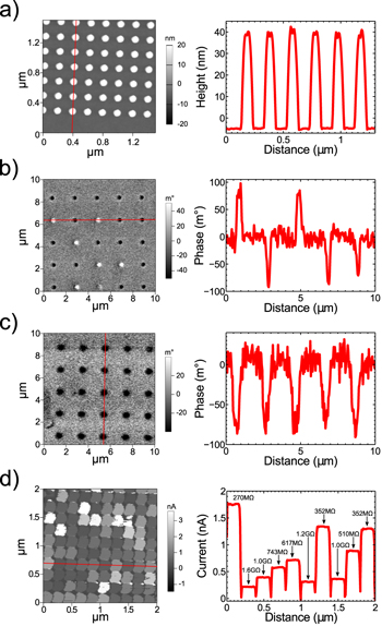
Scanning probe microscopy was used to measure the topography, magnetization and conductivity of the p-MTJ pillars after demagnetization. Figures 6(a) and (b) show AFM topography and corresponding MFM images of an array of pillars made from the Mo/CoFeB/MgO/CoFeB/Mo film, after AC-demagnetization in a perpendicular field. The topography shows a uniform set of pillars with height of about 40–50 nm corresponding to the thickness of the Mo/CoFeB/MgO/CoFeB/Mo/Ru. In the AC-demagnetization process the magnetic field was cycled from about 12 kOe to zero with amplitude decreasing in 0.1% steps. This produced a state in which some pillars were magnetized 'up' and some 'down' but the two layers in each pillar are expected to be magnetized parallel due to their magnetostatic interaction. Therefore only two of the four possible magnetic states of the pillars would be present (the other two states are the antiparallel states which could be produced by minor loop cycling as shown in the TMR data.) The perpendicular anisotropy produced a strong magnetic contrast despite the small thicknesses of the layers, and the images for 500 nm pillars sizes show single domain structure even at this large size.
Figure 6. (a) MFM topography image of patterned Mo/CoFeB/MgO/CoFeB/Mo p-MTJ pillars of 125 nm in diameter and (b) and (c) phase images from the magnetic structure of the same sample of p-MTJ pillars of 500 nm in diameter. (b) shows the pillars after out-of-plane AC-demagnetization and (c) shows the remanent state after saturation in which all pillars are magnetized in the same direction. The color scale represents degrees of phase in the range 1°–1.3°. (d) Current map of an array of p-MTJ pillars of 70 nm diameter from the same sample recorded at +500 mV sample bias.
Download figure:
Standard image High-resolution image
Figure 6(c) demonstrates MFM images of the patterned Mo/CoFeB/MgO/CoFeB/Mo MTJ sample following DC-demagnetization in an out-of-plane field, i.e. the state at remanence after saturation. The p-MTJ pillars all showed a clear dark magnetic contrast which corresponds to the magnetization 'down' state.
Figure 6(d) shows a current map of the same p-MTJ sample (following AC-demagnetization) but from a different area of the sample in which the pillar diameter was 70 nm and spacing was about 100 nm. The pillars are circular in SEM images, but in the cAFM scans the pillar shape is convoluted with the tip shape giving an irregular contour that is the same for each pillar (this tip shape effect precluded cAFM measurements of the block copolymer patterned p-MTJs). Different shades of gray indicate variability of the pillar resistance states, which in one linescan indicated in the figure, varied between 0.27 and 1.6 GΩ. This result shows that despite having well-defined magnetic states in which the magnetization is expected to be parallel giving a low magnetoresistance, the actual resistance varied over a factor of 6 or more. This could originate from differences in pillar area, in the layer structure at the edges formed by ion beam etching, or local variability in the MgO layer which produce a range of resistance values for nominally identical pillars. The contribution from differences in pillar area is expected to be no more than about 10%, based on the size distribution of the pillars from microscopy, and the majority of the variation is therefore attributed to edge effects such as intermixing or variations in the MgO.
4. Conclusions
The EBL fabrication process described here enabled patterning of p-MTJ films into pillars with dimensions of 45 nm and above which were characterized using probe microscopy. A block copolymer process produced 30 nm diameter pillars but the p-MTJ itself was only 17–18 nm across. Pillars of as-grown films with diameter below 1 μm showed a butterfly shaped loop characteristic of orthogonal anisotropy, whereas pillars made from annealed films showed clear switching of the hard and soft layers based on magnetoresistance measurements. MC modeling reproduced the hysteresis behavior based on interacting macrospins including asymmetry in the loops resulting from thermal effects. Minor loops confirmed significant interactions between the hard and soft CoFeB layer which offset the soft layer loop, enabling antiparallel-to-parallel reversal at much lower fields than the parallel-to-antiparallel reversal. AC-demagnetization of pillars produced from annealed films led to ground states in which both magnetic layers were magnetized parallel, and MFM showed single-domain states even for 500 nm diameter pillars. 70 nm diameter pillars measured in the parallel state showed a variation in resistance which was larger than that expected from the size distribution. This is assumed to originate from edge features such as intermixing, resulting from the patterning process or to variations in the MgO layer thickness. These results are relevant to the continued scaling of p-MTJ-based devices into the tens of nm regime.
Acknowledgments
This work was supported by C-SPIN, one of six STARnet Centers of SRC supported by MARCO and DARPA. This work made use of the MRSEC Shared Experimental Facilities at MIT, supported by the National Science Foundation under award number DMR-1419807; in part at the Center for Nanoscale Systems (CNS) at Harvard University, a member of the National Nanotechnology Infrastructure Network (NNIN), which is supported by the National Science Foundation under NSF award no. ECS-0335765. LT is grateful to Richard G Hobbs for valuable discussions. PV acknowledges support from Conicyt, Chile, award no. FBO07, (CEDENNA).