

Abstract
Large-scale integration of MoS2 in electronic devices requires the development of reliable and cost-effective deposition processes, leading to uniform MoS2 layers on a wafer scale. Here we report on the detailed study of the heterogeneous vapor–solid reaction between a pre-deposited molybdenum solid film and sulfur vapor, thus resulting in a controlled growth of MoS2 films onto SiO2/Si substrates with a tunable thickness and cm2-scale uniformity. Based on Raman spectroscopy and photoluminescence, we show that the degree of crystallinity in the MoS2 layers is dictated by the deposition temperature and thickness. In particular, the MoS2 structural disorder observed at low temperature (<750 °C) and low thickness (two layers) evolves to a more ordered crystalline structure at high temperature (1000 °C) and high thickness (four layers). From an atomic force microscopy investigation prior to and after sulfurization, this parametrical dependence is associated with the inherent granularity of the MoS2 nanosheet that is inherited by the pristine morphology of the pre-deposited Mo film. This work paves the way to a closer control of the synthesis of wafer-scale and atomically thin MoS2, potentially extendable to other transition metal dichalcogenides and hence targeting massive and high-volume production for electronic device manufacturing.
Export citation and abstract BibTeX RIS
Introduction
Transition metal dichalcogenides (TMDs), like MoS2, in a few years imposed strongly as an alternative or a complement to graphene, thanks to their inherent semiconducting character [1, 2]. This and other advantages such as high spin–orbit coupling, strong enhancement of photoluminescence (PL) for the monolayer MoS2 and solid-state lubricant properties, open up perspectives for its integration, for instance in spin-electronics, optoelectronics and nanotribology, in addition to its employment in the field of hydrogen storage, catalysis and bio-sensing [3–7].
Mono and few-layers of MoS2 are extensively produced as flakes by means of mechanical exfoliation from bulk geological crystals. However, while effective for prototypical applications [4], this approach poses severe limitations in terms of technology transfer, which necessarily requires the wafer-size synthesis of MoS2 in the thin film form. Therefore, in the last few years the request for a large-area production of MoS2 films with high crystal quality and tunable thickness has involved a number of hybrid chemical vapor deposition methodologies, including thermolysis of (NH4)2MoS4 [8], reaction between MoCl5 and S [9], chemical vapor deposition by reacting MoO3 and S powders [10–12] or Mo metallic films and S vapor [13–16]. Recently, MoS2 and other TMDs were synthesized as extended grains with atomically thin thickness by means of metal–organic CVD [17].
The most popular chemical method is the vapor-phase reaction from MoO3 and S powders, which proved to be an efficient and cost-effective method to synthesize micron-sized MoS2 2D islands with trigonal prismatic structures, as in the exfoliated flakes. However, this method is limited by lateral scaling and lacks a selective control of the MoS2 thickness. These two requisites can be reached by implementing the deposition from a Mo-based solid film source (SFS), pre-grown by physical vapor deposition, yielding a fine-tuning of the MoS2 thickness. Indeed, the number of MoS2 layers can be set as a function of the Mo film thickness [13, 14], therefore the ease and repeatability of the method make it very attractive in terms of manufacturability and technology transfer, being moreover easily extended to other TMDs.
In this paper we present the MoS2 synthesis by using S powder and sub-stoichiometric oxidized molybdenum films as a process of heterogeneous vapor–solid reaction (evaporated source S(g) + SFS Mo(s) → deposited film MoS2(s) + by-products(g)). The chemical details of the Mo SFS and MoS2 film, deduced by photoelectron spectroscopy (XPS) analysis of the Mo 3d, S 2s and 2p core-level photoemission lines, helped in elucidating the process of sulfurization as a surface process of chemisorption, with the outcome that the main properties of the MoS2 films—the thickness control on large scale, can be tuned by changing the Mo SFS thickness and the cm2 coverage.
Moreover, by performing Raman and PL spectroscopies we present a careful analysis of the MoS2 crystal and morphological quality, in terms of the vibrational modes and excitonic radiative recombination, as a function of the sulfurization temperature and of the number of constitutive MoS2 layers. The surface morphology of SFSs and MoS2 layers were finally addressed by atomic force microscopy (AFM) analysis, which allowed us to identify the granular nature of the MoS2 film and to find out a correspondence between the packing of grains and the structural ordering of the layers detected by Raman spectroscopy.
Methods
MoS2 synthesis
MoS2 was synthesized starting from Mo and MoO3 films with tunable thickness (1–4 nm) and grown by means of e-beam evaporation (from Mo foils and MoO3 pellets as sources, respectively) onto 290 nm SiO2/Si and 200 nm AlN/Si substrates. The latter kind of substrates was used for XPS measurements, in order to avoid charging effects. Mo films were put in the center of a quartz tube, inside a furnace. Sulfur powder (1–2 gr, by Sigma Aldrich) is placed in a quartz boat and introduced upstream the quartz tube. This procedure allowed the sulfur powder to start evaporating (around 170 °C) when the substrates were at temperature above 400 °C. An Ar flow of 0.2 to 0.3 l h−1 was used as carrier gas for S vapor towards Mo films. The furnace was heated at 500 °C, 750 °C, or 1000 °C with a 5 °C min−1 rate and, after 10 min at the maximum temperature, the furnace was naturally cooled down.
Characterization
XPS measurements were performed on a PHI 5600 instrument equipped with a monochromatic Al Kα x-ray source (energy = 1486.6 eV) and a concentric hemispherical analyzer. The spectra were collected at a take-off angle of 45° and band-pass energy of 23.50 eV. The instrument resolution is 0.5 eV. The spectra were aligned using C1s (285 eV) as reference.
Raman spectroscopy measurements were performed in a Renishaw In-via spectrometer with a 514 nm (2.41 eV) Ar laser at 1 mW of power.
PL measurements were carried out by using the 532 nm line of a Nd-Yag laser having an excitation power of about 50 mW. The laser spot size on the samples surface was of about 100 μm. The PL emission was dispersed by a 150 l mm−1 diffraction grating of a 500 mm focal length spectrometer. The PL was analyzed by a Peltier cooled CCD detector and the resulting spectral pitch was of about 0.8 meV.
The morphology of the samples was investigated in tapping mode by means of an AFM-Bruker commercial system, equipped with ultrasharp silicon probes (nominal tip radius ∼10 nm). Root-mean-square (rms) roughness and other statistical parameters of the surface morphology were quantitatively derived from the topographies employing the free-available WSxM software.
Results and discussion
Heterogeneous vapor–solid reaction
The identification of the chemical species involved in the MoS2 formation is a key step for the comprehension of the reactions involved in the chemical process of MoS2 synthesis. Thus, XPS measurements were carried out on several SFSs, prior to and after the sulfurization process. The analysis of the SFSs allowed to verify that the evaporated films (1–4 nm thick) are always oxidized across the entire film thickness, oxidation occurring during the film transfer from the deposition chamber to the sulfurization furnace. Figure 1(a) shows the Mo 3d XPS line measured in a SFS obtained from evaporation of Mo foils. For comparison, we report also the Mo 3d XPS line in a film evaporated from MoO3 pellets (figure 1(b)). According to the XPS line deconvolution strategy proposed in [18], figure 1(a) shows that no purely metallic Mo is present and the Mo film undergoes oxidation into four different oxidation states, namely Mo6+, Mo5+, Mo4+, Mo2+, with a slightly higher prevalence of the Mo6+ and Mo4+ species at the surface level and a slight prevalence of Mo5+ and Mo2+ at the interface with the substrate, according to an angle-dependent XPS analysis. On the other hand, the Mo 3d XPS line of the SFS grown from MoO3 pellets (figure 1(b)), shows the dominance of the Mo6+ bonding state (corresponding to MoO3) with a minor component of the Mo5+ one (Mo2O5). The XPS analysis of the same films but after sulfurization at 750 °C is shown in figures 1(c)–(f), respectively. The XPS peaks reveal the prevalence of MoS2 arranged in the more stable trigonal prismatic (Mo2H) phase. This is highlighted by the presence of the Mo4+ 3d5/2 and Mo4+ 3d3/2 components on the Mo 3d line and by the S 2p1/2 and the S 2p3/2 components in the S 2p line. Additional minor components are also observed and attributed to the octahedral phase (Mo1T) and to oxide species (Moox).

Figure 1. Left column: XPS profiles of Mo atoms binding energy for e-beam evaporated (a) Mo film (from foils), (b) MoO3 film (from pellets). Right column: XPS profiles of MoS2 layers obtained from Mo film (from foils), in particular the binding energies of (c) Mo atoms and of (d) S atoms; XPS profiles of MoS2 layers obtained from MoO3 film (from pellets), (e) Mo atoms and (f) S atoms.
Download figure:
Standard image High-resolution imageBased on the integral area subtended by the Mo 3d and S 2p peaks (normalized to the corresponding sensitivity), the concentration of Mo atoms in MoS2 are 0.33 ± 0.20 for the sample of figures 1(c) and (d) and 0.36 ± 0.20 for that of figures 1(e) and (f), meaning that the MoS2 films obtained from pre-deposited Mo and MoO3 are both stoichiometric.
XPS results clearly indicate that the MoS2 synthesis takes place irrespectively of the different Mo oxides stoichiometry. In agreement with previous studies [12, 15], our experimental observations are consistent with a sulfurization of MoO3 through intermediate reactions, which reduce the Mo oxidation states. Indeed, the reaction conveyed in equation (1) [10, 19]:

is the result of two steps (equations (2) to (3)):


where reaction (2) is the S-induced reduction of the MoO3 in sub-stoichiometric oxide leading to SO2 by-product, and reaction (3) is the effective one for the MoS2 production, from MoOx species.
Moreover, considering that the sublimation temperature for MoO3 is around 700 °C [20], the reaction between stoichiometric Mo oxide and sulfur vapors can take place only above this temperature. The formation of MoS2 at low temperature [10, 12] can be justified only considering the intermediate reaction of equation (2), which releases MoOx intermediate products, as observed by [19]. Indeed, in the latter case it is not necessary to have MoO3 vapor, since the presence of sulfur atoms in proximity of molybdenum oxide powder is sufficient to prompt the reactions in equation (2). For the same reason, when the Mo precursor is in the film form (MoOx), the MoS2 synthesis has been observed already at 500 °C [16]. However, for sulfurization temperatures above 700 °C, Mo oxide sublimation takes place also in the SFS, representing a competitive reaction to sulfurization; thus, in order to favor sulfurization, it is necessary to operate in a sulfur-saturated environment.
The mechanism of MoS2 formation driven by pre-existing MoOx can be described as a heterogeneous vapor–solid reaction, where the S chemisorption takes place at the film surface because S atoms are selectively absorbed to MoOx nucleation sites in the SFS. From this description, there are consequences on the details of the grown MoS2. As an example, in the case of both MoO3 and S gaseous reactants, Mo–S bonds are probably formed in the vapor and then the material lands on the substrate and nucleates wherever there are borders, rough surface [21] or seed molecules [10, 22], therein forming triangular shaped MoS2 islands, which may eventually serve as seed for a successive layer growth. In the present case of the heterogeneous reaction, the whole pre-existing MoOx film acts as a seed for the MoS2 growth. As such, the Mo–S reaction is allowed to proceed as long as the selective nucleation sites are saturated according to equations (1)–(3) and to the pictorial sketch of figure 2.

Figure 2. Pictorial sketch of the growth mechanism for the heterogeneous vapor–solid reaction between S vapor and MoOx SFS.
Download figure:
Standard image High-resolution imageThis would clarify why the number of the grown MoS2 layers resulted to be highly reproducible and determined by the starting MoOx layer thickness, notwithstanding a potential Mo loss during sulfurization, whose detection requires deeper studies. A direct consequence is that the MoS2 layer uniformity throughout the whole sample area is directly implicated by the uniformity of the SFS (see figure S1 of supporting information). As a result, the method is potentially suitable for a wafer-scale production of laterally uniform MoS2 films with a tunable number of layers.
This aspect is highlighted also by the Raman spectroscopy analysis of a MoS2 film grown at 1000 °C, from a SFS with nominal thickness of 4 nm. The Raman spectrum in figure 3(a) is decomposed into in-plane  and out-of-plane A1g phonon modes, whose frequency separation is indicative of the number of MoS2 layers [23]. The two modes are centered at 407 and 383 cm−1, with a frequency difference Δω of 24 cm−1, corresponding to a four-layer (4L) MoS2. The homogeneity of the films is elucidated by the 10 × 10 μm2 scale Raman maps, reported in figures 3(b) and (c), where the
  and A1g frequency is plotted as a function of the lateral x–y position. The uniformity was repeatedly checked in spatially separated regions of the sample. It can be noticed that the signal dispersion inside the map is below 0.5 cm−1, confirming a uniform thickness throughout the whole sample.
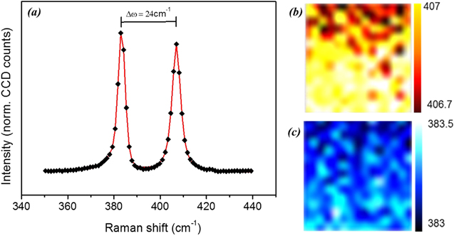
Figure 3. (a) Raman spectra of a four-layer MoS2 film grown at 1000 °C, with the corresponding distance between  and A1g peaks Δω. Raman maps of (b)
  peaks (yellow–red colored) and (c) A1g peaks (blue colored), of a sample area of 10 × 10 μm2.
Download figure:
Standard image High-resolution imageThe presence of extended and continuous MoS2 nanosheets throughout the 4L-MoS2 samples grown at 1000 °C is highlighted by the cross-view transmission electron microscopy images reported in figure S2 of the supporting information. In the inset, a zoomed portion of the image allows evaluating the separation between adjacent layers in the range of 0.65–0.70 nm in good agreement with the theoretical value. The thickness of the grown nanosheets is 2.8 nm confirming the thickness estimation (4L) derived by the Raman analysis.
Influence of the deposition temperature on the MoS2 properties
The heterogeneous vapor–solid reaction can allow the MoS2 growth at lower deposition temperature, Td, compared to those required in a MoO3 and S gaseous reaction. On the other hand, the corresponding thermal budget supplied to the system at Td can be anyway critical in dictating the structural quality of the deposited MoS2.
Figures 4(a)–(c) show the Raman spectra of MoS2 films grown at 500 °C, 750 °C and 1000 °C respectively, from a 4 nm thick SFSs. They are all characterized by the same wavenumber difference Δω between the A1g and  phonon modes that stems for the same thickness of 4L-MoS2, despite the different deposition temperatures. However, the Raman spectrum of the sample grown at low temperature exhibits significant asymmetric broadening, whereas a symmetric profile is observed whenever the deposition temperature is increased.
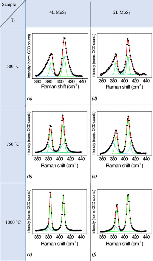
Figure 4. Raman spectra of MoS2 films grown from different precursor thicknesses ((a)–(c) from 4 nm, (d)–(f) from 2 nm of MoOx) and different temperatures ((a) and (d) at 500 °C, (b) and (e) at 750 °C, (c) and (f) at 1000 °C). Black symbols are experimental data, red curve is the fitting curve obtained by using Gaussian–Lorentzian mixed curves (green curves are for o-Vf components of the  and A1g modes, blue curves are for d-Vf ones).
Download figure:
Standard image High-resolution imageIn order to take into account the asymmetric broadening, each of the A1g and the  peaks were fitted with two pseudo-Voigt curves. The use of the Voigt fitting function is typical for the Raman modes of MoS2 with trigonal-prismatic structure. The presence of asymmetric tails on the A1g and the
  peaks is usually related to the disorder-induced relaxation of Raman selection rules. More in detail, as described in [24], a downshift of the
  peak resembles the dispersion of the longitudinal optical (LO) and transverse optical (TO) branches moving away from the Γ point of the Brillouin zone. Instead, for the A1g peak the dispersion of the out-of-plane optical (ZO) branch predicts an upshift. In particular, the presence of defects in the MoS2 crystal activates zone-edge phonons such as the LO phonons at the M point, LO(M) at ∼380 cm−1, the TO(M) at ∼360 cm−1 and the ZO(M) at ∼410 cm−1 [24].
For simplicity, the fitting curve of each asymmetric tail will be labeled as disordered-Voigt function (d-Vf), since it takes into account for all the disorder-activated components decorating the  and A1g peaks. The fitting components related to the trigonal-prismatic structure will be labeled as ordered-Voigt function (o-Vf). In table 1 we report as a function of Td the
  and the A1g peaks position, their FWHM and the relative intensity ratio, along with the d-Vf/o-Vf area ratio.
Table 1.
Values of Raman  and A1g peaks position, FWHM, d-Vf/o-Vf weight ratio in each peak and
  relative intensity ratio for 4L- and 2L-MoS2, as a function of the deposition temperature Td.
| 4L-MoS2 | 2L-MoS2 | |||||
|---|---|---|---|---|---|---|
| 500 °C | 750 °C | 1000 °C | 500 °C | 750 °C | 1000 °C | |
 peak position (cm−1) peak position (cm−1) |
384.2 | 383.5 | 383 | 384.2 | 385.3 | 386.5 |
 peak FWHM (cm−1) peak FWHM (cm−1) |
15.2 | 7.2 | 4.3 | 10.8 | 9.7 | 6.0 |
| d-Vf/o-Vf area ratio | 1.8 | 0.8 | 0.2 | 3.3 | 1.5 | 0.5 |
| A1g peaks position (cm−1) | 407.1 | 405.8 | 407 | 405.8 | 406.9 | 406.9 |
| A1g peaks FWHM (cm−1) | 9.5 | 6.5 | 4.6 | 7.2 | 7.7 | 6.5 |
| d-Vf/o-Vf area ratio | 2.0 | 0.6 | 0 | 2.4 | 0.35 | 0 |
 intensity ratio intensity ratio |
0.6 | 0.7 | 1.04 | 0.6 | 0.6 | 0.7 |
At Td = 500 °C the MoS2 Raman profile shows a strong asymmetric broadening of the peaks (figure 4(a)) which claims for d-Vfs having a double area with respect to that of the o-Vf components. Upon increasing the deposition temperature up to 750 °C (figure 4(b)), the area of the d-Vfs is significantly reduced. A further increase of the temperature up to 1000 °C leads to the suppression of the d-Vf in the A1g mode (sensitive to the vertical packing of the layers), while in the  peak the d-Vf component is still present, but with a strongly decreased area (see also table 1). This observation makes evidence that by increasing the temperature it is possible to obtain a high degree of out-of-plane order, i.e. the MoS2 film is vertically packed as the geological counterpart. Remarkably, the presence at 1000 °C of the d-Vfs component for the
  mode highlights that in-plane defects, such as line defects and grain boundaries, are still present.
Intriguingly, when considering the  intensity ratio as a function of temperature (table 1), we observe that it remains below 1 for Td equals to 500 °C and 750 °C, while it is above 1 for Td = 1000 °C, the latter being close to the one commonly observed in geological MoS2. An
  ratio below 1 has been reported by several authors as the fingerprint of the absence of doping in chemically grown samples [25]. This picture arises from the observation made by Chakraborty et al [26] about the softening and broadening of the A1g phonon with electron doping during in situ Raman measurement of top-gated monolayer MoS2 field-effect transistors. However, we consider that the
  intensity ratio and the apparent reduction of the broadening-related components observed in the Raman spectra at high temperatures can be more convincingly associated with a higher degree of structural order of the MoS2 films in both the in- and out-plane direction. Similar conclusions have been reported in [16, 27], where the change of the
  ratio to values above 1 were obtained in samples thicker than our 4L-MoS2 and chemically grown on ultra-smooth c-plane sapphire at high Td (≥900 °C). In those cases, the atomic-scale flat substrate promotes the growth of MoS2 micro-terraces with high structural order in the in-plane direction, therein resulting in a narrow and enhanced
  Raman modes. Analogous results had not been observed yet in MoS2 grown on SiO2/Si substrates.
We applied the same analysis for MoS2 films obtained from 2 nm thick Mo SFSs, and grown as the previous set at 500 °C, 750 °C and 1000 °C (figures 4 (d)–(f), and table 1). In these spectra the frequency separation Δω of the modes is equal to 21 cm−1, indicative of bilayer (2L) MoS2 films.
In these bilayers the shape of the Raman peaks has a similar dependence upon the deposition temperature observed for the 4L-MoS2 series. In more detail, the Raman spectra of the 4L- and the 2L-MoS2 films grown at 500 °C compares well, (figures 4(a) and (d), respectively). On the contrary, for the deposition temperature of 750 °C and 1000 °C, the  peaks of the 2L-MoS2 films show a d-Vf component with a weight (i.e. area) higher than in the 4L-MoS2
  peaks (figures 4(b), (c), (e) and (f)). At Td = 1000 °C the d-Vf of the A1g disappears in both 4L-MoS2 and 2L-MoS2, (figures 4(c) and (f) and table 1), but the
  intensity ratio in 2L-MoS2 remains below 1.
Since the symmetry of the Raman peaks shape is the hallmark of a high structural quality of the materials, two important consequences can be deduced: (1) the MoS2 structural quality increases with increasing the deposition temperature, irrespective of the layers number; (2) the discrepancy between the Raman spectra of the 4L- and 2L-MoS2 grown at 1000 °C indicates the dependency of the MoS2 structure (i.e. crystalline organization) on the grown layers number. In particular, the discrepancies detected between the 4L- and 2L-MoS2 Raman spectra indicate that the former sample has a higher in-plane order. This observation puts a warning in the thickness of MoS2 chemically grown on silicon substrates from SFS, underlining that the best qualities in term of crystalline ordering can be obtained overcoming the two layers.
In order to gather further insights into the properties of the MoS2 films, we have carried out a PL spectroscopy investigation as a function of the deposition temperature and of the number of layers.
PL measurements highlight an improvement of the optical properties with increasing deposition temperature (figure S3 in supporting information) for both 4L- and 2L-MoS2 films. In particular, as summarized in figure 5(a), both 4L- and 2L-MoS2 films grown at 1000 °C show two well-defined emission peaks in the PL spectra acquired at room temperature, which are ascribed to A and B excitonic recombination [1, 28].

Figure 5. (a) Photoluminescence at room temperature of the 2L- (red line) and of the 4L- (blue line) MoS2 grown at 1000 °C. The arrows indicate the position of the emission peaks due to excitonic recombination A and B. (b) PL profiles as a function of the temperature for 4L-MoS2 grown at 1000 °C: in the inset the position of the excitonic A peak is plotted as a function of temperature.
Download figure:
Standard image High-resolution imageIt is worth noticing that, although the bilayer does not possess an optimized structural quality, it shows the expected PL intensity increase and blue shift of the A peak, resulting from the decreased number of layers as compared to the 4L sample. The room temperature PL comparison between the 4L and 2L films indeed supports the structural identification provided by the Raman analysis. In addition, we gathered a deeper understanding of the optical properties of the 4L-MoS2 sample by performing measurements as a function of the lattice temperature (figure 5(b)). This analysis confirms the attribution of the observed spectral features since the peak energy of A and B excitons follows the temperature dependent band-gap narrowing of the direct gap [29, 30].
Morphology
Both PL and Raman data confirm the dependency of the crystallinity quality on the deposition temperature and on the number of layers. These observations can be related to the MoS2 morphology, which in turn depends on the SFS morphology.
To gain a deeper understanding in this respect, we performed AFM investigations starting from the 2 nm thick SFS and its corresponding 2L-MoS2 grown at 750 °C (figures 6(a) and (b), respectively). The topography of the MoOx film reveals it is continuous and completely covers the surface being constituted by grains with main size of 20–30 nm. A quantitative estimation of the height distribution is provided by the rms roughness value, which is around 0.3 nm. In the 2L-MoS2 morphology of figure 6(b), we recognize grains with main size of 20–30 nm, but the film presents also an enhanced vertical dynamic (4 nm) and roughness (0.7 nm), the latter corresponding to the thickness of one MoS2 layer.
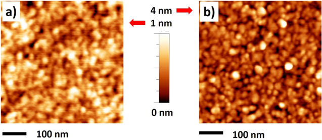
Figure 6. AFM topographies of the: (a) 2 nm thick SFS, (b) 2L MoS2 film obtained at 750 °C.
Download figure:
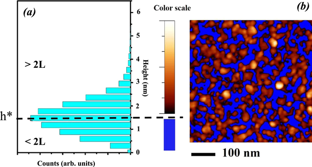
Standard image High-resolution imageIn figure 7(a) we report the height histogram of the MoS2 topography. The mean height is around 1.4 to 1.5 nm, which corresponds to the theoretical thickness of a 2L-MoS2 film, in agreement with the thickness estimation derived by Raman spectroscopy. In figure 7(b) is reported the AFM topography of figure 6(a) after a 'flooding' filter. The filter excludes surface points below a given height threshold h* which we have set at 1.4 nm, leaving points with height equal (or higher) than 1.4 nm. Since the Raman technique in this sample detects a signal only due to 2L-MoS2 upon the whole sample area, the flooded AFM image shows only MoS2 surface features that can contribute to the Raman signal of a 2L film, while excluded points are plotted in blue. The MoS2 structures are densely and randomly distributed over the entire scanning area. Nevertheless, the film is characterized by an in-plane morphological disorder, in particular the MoS2 structures are disconnected and organized in isolated grains and grain chains with poly dispersed size. The presence of a large density of grain boundaries can be directly linked in to the d-Vf components of the Raman modes. In fact, it is known that at the grain boundaries the symmetry of the crystalline material breaks and the atoms typically react with the environment. Both these conditions lead to a modification of the Raman modes which differ from those of the perfect crystal in shape (asymmetric tails) and width (broadening) [31].
Figure 7. (a) Height histogram and (b) flooded image of the AFM topography shown in figure 6(b). The threshold of the flooding filter (h*) has been set at 1.4 nm which is the theoretical thickness of a 2L-MoS2 film.
Download figure:
Standard image High-resolution image
For the 4L-MoS2 grown at 750 °C, the AFM images (figure S4(a) in supporting information) show the presence of grains with mean size comparable to those of the SFS and rms roughness of 0.4 ÷ 0.5 nm (lower than the 2L case). Nevertheless, the analysis based on the flooding filter reveals that in the 4L-MoS2 film the grains are more densely packed, forming in-plane connected layers with a residual superficial roughness. The flooded image (figure S4(b) in supporting information) shows that almost all the surface points are below the height threshold, which has been set at the theoretical thickness of the 4L-MoS2 (the image looks like blue colored). Reasonably, the bottom of the 4L-MoS2 is not reached by the AFM tip due to the presence of densely packed MoS2 grains. As a direct consequence, the better in-plane order of the MoS2 layers leads to a reduction of the area of the d-Vf components in the 4L-MoS2 Raman spectra with respect to the 2L-MoS2.
The AFM analysis allows us to draw further conclusions about the SFS-based synthesis of MoS2. We can reasonably suppose that the vapor/solid (sulfur/SFS) reaction occurs in preferential sites of the SFS represented by the MoOx grains, since similar granular nature is observed both in the SFS and MoS2 topographies. Thus, the SFS morphology plays a crucial role in determining the structure and morphology of the MoS2 layers. In particular, the granularity and surface roughness of the SFS grown on SiO2/Si represent a limiting factor in the synthesis of well-ordered ultra-thin bilayer film, while for the thicker samples (4L) the influence of the SFS morphology becomes less relevant.
Conclusions
We have shown that a SFS consisting of sub-stoichiometric Mo oxide species undergo sulfurization in MoS2 via heterogeneous vapor–solid reaction, through intermediate and sequential chemical reactions. In the SFS sulfurization the S atoms are selectively chemisorbed by MoOx nucleation sites in the SFS, and this reaction is accessible also at low temperature (i.e. 500 °C). The use of SFS enables us to have a MoS2 growth with a close control of its atomic thickness by tuning the SFS thickness and in turn with a uniform sample coverage.
If on the one hand we obtained MoS2 already at temperatures as low as 500 °C, on the other we have shown that the structural quality of the material dramatically depends on the deposition temperature. In particular, a detailed Raman analysis of the MoS2 films allowed us to identify in the Raman modes contributions due to structural disorder, both in the in-plane direction and in the vertical packing of the MoS2 layers, whose amount was temperature-dependent. The highest degree of crystallinity is reached at the deposition temperature of 1000 °C, verified by Raman and by PL signature of A and B excitons.
Finally, the structural quality of MoS2 has been observed to depend also on the number of the grown layers. In fact, the best crystalline ordering are achievable by growing 4L-MoS2, as results from a  Raman mode intensity ratio above 1.
The thickness dependence of the MoS2 structural properties is directly connected with the observed granularity of the MoS2, which in turn derives from the SFS morphology. The basic mechanism governing the crystalline order of the grown MoS2 is found out to rely on the connection–disconnection between adjacent grains.
The present results evidence the potential of using the heterogeneous vapor–solid reaction process to synthesize MoS2 films on SiO2/Si substrates, reporting the optimal conditions to achieve the growth of stoichiometric and uniform MoS2 on a large-scale.
Acknowledgments
The authors would like to thank Dr Stefano Brivio (MDM-IMM) for preliminary AFM measurements, Dr Grazia Tallarida (MDM-IMM) for her support on AFM technical use and measurements and Paolo Targa (STMicroelectronics-Italy) for TEM images. The authors also thank Dr Emiliano Bonera (UNIMIB) for fruitful discussion.