
Abstract
We report low-cost conductometric gas sensors that use an ultrathin film made of graphene oxide (GO) nanoflakes as transducing element. The devices were fabricated by lift-off metallization and near-room temperature, atmospheric pressure electrospray printing using a shadow mask. The sensors are sensitive to reactive gases at room temperature without requiring any post heat treatment, harsh chemical reduction, or doping with metal nanoparticles. The sensors' response to humidity at atmospheric pressure tracks that of a commercial sensor, and is linear with changes in humidity in the 10%–60% relative humidity range while consuming <6 μW. Devices with GO layers printed by different deposition recipes yielded nearly identical response characteristics, suggesting that intrinsic properties of the film control the sensing mechanism. The gas sensors successfully detected ammonia at concentrations down to 500 ppm (absolute partial pressure of ∼5 × 10⁻⁴ T) at ∼1 T pressure, room temperature conditions. The sensor technology can be used in a great variety of applications including air conditioning and sensing of reactive gas species in vacuum lines and abatement systems.
Export citation and abstract BibTeX RIS

Content from this work may be used under the terms of the Creative Commons Attribution 3.0 licence. Any further distribution of this work must maintain attribution to the author(s) and the title of the work, journal citation and DOI.
Introduction
Conductometric gas sensors, based on semiconducting metal oxide films, are widely used due to their simplicity, flexibility in production, and broad applicability to many fields [1]. Typically, the adsorption of a gas molecule on the surface of a metal oxide alters surface electronic properties, causing a change in electrical conductivity [2]. Although many metal oxides could be used for gas sensing, only a few show the appropriate combination of adsorption ability, catalytic activity, sensitivity, and thermodynamic stability. These select metal oxides (e.g., SnO2, TiO2, and ZnO), however, are the least active from the catalytic point of view [3]. To alleviate this problem, doping with redox-active noble metal nanoparticles, such as Pt, Au, and Pd, is commonly done to enhance conductivity response and gas sensitivity [4]. Unfortunately, noble metals are expensive, thereby precluding their use in low-cost applications.
Additive manufacturing refers to a group of processes that fabricate freeform structures by successively depositing layers of materials according to a digital model [5]. Additive manufacturing started as a visualization tool of passive, mesoscaled parts. However, recent improvements in the resolution capabilities of the 3D printers, as well as in the recent demonstration of printable active, i.e., transducing, feedstock, additive manufacturing has become a fabrication technology that could address the complexity, three-dimensionality, and material processing compatibility of certain micro and nanosystems [6]. The development of micro and nanoscaled printing technologies is motivated in part by the possibility to harness the properties of materials as their constitutive granularity miniaturizes; for example, metal nanoparticles have lower melting point than bulk metals, which can be used to print metal lines that are sintered at a lower temperature and hence be compatible with low-temperature microsystem manufacturing [7]. In addition, nanoparticles tend to be more stable and resilient to surface oxidation compared to corresponding bulk materials.
Several additive manufacturing technologies have been investigated for the fabrication of micro and nanosystems. The majority of the work has focused on inkjet printing, either piezoelectric based (where the mechanical vibration of a piezo structure overcomes the surface tension of the liquid feedstock to generate droplets [8]) or thermal based (where a heater inside a cavity creates bubbles from the liquid feedstock, which push droplets out of the cavity through a nozzle [9]). In general, piezoelectric implementations are favored because they are compatible with temperature-sensitive feedstock (e.g., biological material) and because the structure of thermal inkjet printing heads is more complex. Also, pen approaches have been investigated, including dip-pen nanolithography (where solid needles are coated with liquid feedstock [10]) and nano fountain pen manufacturing (where hollow needles deliver liquid feedstock from a pressurized plenum [11]). Unlike the tens-of-microns resolution of inkjet printers, pen-based approaches easily achieve submicron resolution. However, unlike inkjet printing methods, the pen hardware makes contact with the printed substrate, which can cause cross-contamination of the printing head and/or attrition of the printing tip. In addition, fabrication via electrohydrodynamic jetting (i.e., electrospray) has recently received attention as a promising candidate for production of low-cost micro and nano-systems because of its capability to create thin films of high quality without involving the extreme conditions of standard semiconductor processing (i.e., high vacuum and/or high temperature) [12]. Electrospray printing also allows for more precise control of the film properties compared with the other techniques, is compatible with low-cost, large-area manufacturing through massive emitter multiplexing [13], and can use a great variety of liquid suspensions as feedstock. In addition, high-resolution electrohydrodynamic printing can overcome the resolution of inkjet printing, although the construction of these advanced printing heads is complex [14].
An attractive substitute active material for conductometric gas sensing is graphene oxide (GO) because of its high sensitivity to reactive gases and harsh environment compatibility. There have been numerous studies of thin-film chemical sensors fabricated by drop-casting, spray coating, spin coating, and inkjet printing suspensions of graphene, GO, and reduced graphene oxide (rGO) in a variety of solutions [15–23]. In particular, electrosprayed graphene, GO, and rGO thin-film structures have been reported for supercapacitor electrodes [24], resistive switch applications [25], and humidity sensors [26].
In this work, low-cost GO gas sensors are reported. The devices have a ∼50 nm thick transducing element fabricated at low temperature (<65 °C) using electrospray printing of GO nanoflakes with a shadow mask, and no post treatment to the devices was conducted—including annealing and doping. Devices with multiple electrode configurations were fabricated on SiO2-coated Si substrates using contact photolithography and the lift-off technique. Our devices were characterized as humidity sensors using a home-built environmental chamber at atmospheric pressure while varying the relative humidity (RH) between 10% and 60%; the response was benchmarked using a commercial humidity sensor. Our devices were also characterized as sensors of ammonia in vacuum at room temperature and ∼1 T pressure; ammonia was chosen for this study because it is a gas commonly used in the semiconductor industry.
In comparison to the published work on electrosprayed rGO humidity sensors [26], our sensors were fabricated with GO nanoflakes in an aqueous suspension versus rGO in isopropanol; also, our sensors implement a four-point probe electrode structure with a total active area that is an order of magnitude smaller than the rGO two-point structure reported in [26]; moreover, our sensors stabilized more than 30 times quicker at 50% RH, and were shown to detect ammonia in addition to RH in air.
Electrospray printing experiments
A custom-built electrospray printer (figure 1, left) was employed to deposit at atmospheric pressure GO thin films onto substrates using a liquid feedstock composed of GO nanoflakes in an aqueous suspension. The liquid feedstock is delivered via a syringe pump to a blunt hollow stainless steel needle with a 300 μm inner diameter. The starting feedstock is a commercial GO solution (Sigma Aldrich product 777676) with a concentration of 4 mg ml−1 GO in water. The original feedstock was diluted using deionized water to concentrations in the 1–40 μg ml−1 range. A grounded stainless steel annular electrode with a circular aperture is positioned in the plane of the tip so that the axis of the tip falls at the center of the electrode aperture, and a high-voltage power supply biases the needle at 3 kV to produce droplet emission. The emitter-extractor design with the substrate placed above the emitter outlet was chosen to discriminate against most of the larger droplets, which tend to strike the annular electrode, leaving primarily the fine micron and submicron droplets for acceleration toward the substrate [12]. The substrate that receives the imprint is on a temperature-controlled heated plate, and the assembly is mounted on a PC-controlled three-axis stage above the needle. To conduct a film deposition, the substrate is first mounted on the heated stage and brought to temperature for about 5 min. The GO nanoflake solution is then loaded into the syringe pump, and the system is primed up to the tip of the emitter. After this, the syringe pump is activated, delivering a flow rate around 1 μl min−1, and a high bias voltage is applied to the tip and adjusted to yield a stable Taylor cone (figure 1, right). The beam of GO droplets is positioned to the side of the substrate and observations are made to ensure that the emission is stable. Finally, a deposition recipe (i.e., a sequence of commands that move the stage in a pre-established fashion) is run.
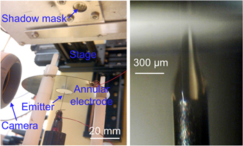
Figure 1. Custom-built electrospray printer (left) and close-up of electrospray emitter when activated (right).
Download figure:
Standard image High-resolution imageOptimization experiments with the home-built electrospray printer were conducted to deposit interconnected films by keeping constant the flow rate and bias voltage while varying the separation distance, stage speed, number of passes, and surface temperature. From these experiments, the optimum separation distance was found to be 3 cm. From the imprints collected, the beam divergence of the electrospray is estimated at 10° semi-angle, in agreement with the literature on cone-jet electrospray sources [27–29]. Average film thicknesses down to 30 nm were measured using a Dektak profilometer (figure 2). Films deposited at temperatures slightly above room temperature (50–64 °C) were of better quality than those deposited at room temperature; in particular, heated samples had less thickness variation across the coating (figure 3) and did not show the liquid accumulation at the edges of the imprints created on unheated samples. Figure 4 is an optical micrograph of an electrosprayed GO film deposited on top of a 300 nm SiO2 film on a Si substrate. The interconnected network of GO nanoflakes is strikingly visible in the optical micrograph; this result is in agreement with previous reports of individual sheets of one-atomic layer-thick graphene films on top of 300 nm thick silicon oxide that become visible in an optical microscope due to a light interference-like effect [30]. Using an atomic force microscope (AFM), a higher resolution image of the distribution of GO nanoflakes over a 25 μm × 25 μm area was captured the nanoflake structure shown by the image is very similar to the structure shown by the optical micrograph (figure 5).

Figure 2. Average GO film thickness versus stage speed. In these experiments three passes of the electrospray emitter across the surface were conducted.
Download figure:
Standard image High-resolution image
Figure 3. Profile of GO film with average thickness of ∼50 nm.
Download figure:
Standard image High-resolution image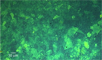
Figure 4. Optical micrograph of GO film with sub-100 nm average thickness.
Download figure:
Standard image High-resolution image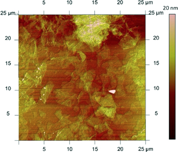
Figure 5. AFM image of a 25 μm × 25 μm area of electrospray printed GO film.
Download figure:
Standard image High-resolution imageOriginally, a single shadow mask (stainless steel, 250 μm thick, 1.3 mm diameter aperture) was used to create the imprints. However, during operation of the electrospray emitter the GO solution wetted the perimeter of the aperture of the shadow mask, and upon drying and mask removal, freestanding walls of GO nanosheets were left on some areas around the edge of the hole, and patches of the imprint were delaminated from the substrate in other areas. To prevent edge sidewall formation and imprint delamination, a two-layer shadow mask was implemented (two stainless steel sheets, each 125 μm thick, bottom layer 1.3 mm diameter aperture, top layer 1.0 mm diameter aperture, concentrically mounted). With the two-layer shadow mask and under optimized conditions, GO films with average thickness <100 nm were successfully manufactured.
Device fabrication
The process flow to fabricate the GO gas sensors is shown in figure 6. The starting substrate is a 1 cm-wide square piece of single-crystal silicon coated with 500 nm of thermal oxide. First, image reversal contact lithography is conducted in a spun-coated thin film of photoresist to transfer the layouts of the electrodes; after development, the patterned photoresist film is inspected to insure that the exposed areas were free of photoresist. Next, a 100 nm thick Au film on top of a 10 nm thick Cr film is deposited everywhere on the substrate using the electron beam evaporation technique. The photoresist is dissolved using acetone, removing the metal stack everywhere on the substrate except on the features defined by the lithography, thereby manufacturing the sensor electrodes by the lift-off technique. The fabrication of the device is completed by electrospraying a suspension of GO nanoflakes on top of the electrodes while the substrate is slightly heated. The completed sensor chips were placed in standard IC packages with Au wire-bonds (figure 7).
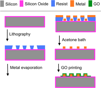
Figure 6. Process flow schematic to fabricate conductometric GO gas sensors.
Download figure:
Standard image High-resolution image
Figure 7. A completed chip with a wired GO gas sensor with four-point probe electrode configuration. The GO film is the greenish dot below the center of the chip pointed out with an arrow.
Download figure:
Standard image High-resolution imageFor the sensors with the smallest electrode structure studied, the devices have an active area of about 0.03 mm2 between the two inner electrodes (0.076 mm2 total active area); the metallization lines underneath the active area are 10 μm wide with 50 μm separation (figure 8).

Figure 8. Optical micrograph of a fabricated conductometric GO gas sensor with a four-point probe electrode configuration, and an inset that shows a close-up view of the active area of the sensor (top left corner). The images were taken after characterization the device; the electrodes appear to have degraded in some areas after exposure to reactive gases and currents in excess of 20 μA.
Download figure:
Standard image High-resolution imageCharacterization of the devices as humidity sensors
The packaged sensors were placed inside a custom-built environmental chamber (figure 9, left) where the RH was varied between 10% and 60%. A commercial humidity sensor (Honeywell HIH-4000) was mounted near the GO sensor for comparison (figure 9, right). In the standard four-point probe configuration of the GO sensor, current was supplied to electrode 1 with a source-measuring unit (SMU) Keithley 2612B, electrodes 2 and 3 were floating, and electrode 4 was connected to ground. The resistance across pins 2 and 3 was calculated using the formula R23 = (V2 − V3)/I1. Through experimentation, it was determined that an optimal current value of 2 μA supplied to electrode 1 yielded the largest difference in voltage between electrodes 2 and 3. Voltage readings of the electrodes were logged on the GO sensor and the commercial humidity sensor with a Dataq DI-149, which is an eight-channel data logger that samples data at a rate of 20 Hz. The outputs from the GO devices had large signal-to-noise ratios; therefore, signal processing was not required.

Figure 9. Home-built environmental test chamber (left); close-up of GO sensor in the foreground and commercial sensor in the background (right).
Download figure:
Standard image High-resolution imageWe conducted two kinds of experiments to characterize the devices as humidity sensors. In the first kind of experiments we characterized dynamically the GO sensors, that is, we benchmarked the capability of the printed sensors to track the RH as it 'quickly' changed within the chamber of the apparatus (time scale on the order of tens of seconds). Figure 10, left shows the dynamic response as humidity sensor of two different GO devices, i.e., GO1 and GO2 (orange and red curves, respectively); the dynamic response of the commercial sensor while each printed sensor was characterized is also reported (green and blue curves, respectively). The GO sensors were made with slightly different printing recipes, described in table 1, which yielded devices with different GO film thicknesses. From these experiments it is concluded that the dynamic response of the GO sensors closely tracks that of the commercial sensor. As a comparison, our electrospray-printed GO sensors stabilize with humidity in less than 1 min versus the much longer stabilization times (>30 min in most cases) of the electrosprayed rGO sensors reported in [26].

Figure 10. Dynamic response to humidity of two electrospray-printed GO devices compared with a commercial sensor (left) and sensor resistance versus humidity of the same electrospray-printed GO devices (right).
Download figure:
Standard image High-resolution imageTable 1. Details of the electrospray printing recipes used to make the two GO sensors tested for response to humidity.
| Sample | GO dilution (μg ml−1) | Flow rate (μl min−1) | Surface temperature (°C) | Stage separation (cm) | Stage speed (mm s−1) | Passes per line (#) | Lines (#) | Line spacing (mm) |
|---|---|---|---|---|---|---|---|---|
| GO1 | 2 | 2 | 64 | 3 | 0.22 | 5 | 8 | 0.3 |
| GO2 | 20 | 2 | 60 | 3 | 0.22 | 1 | 24 | 0.1 |
In the second kind of experiments we characterized the relationship between the resistance of the sensors and the RH. A linear relationship between the resistance of the GO sensors and the RH in the 10–60% range was measured (figure 10, right); the similarity between the linear response of the two devices, considering that they were fabricated with different electrospray printing recipes, suggests a common underlying physical sensing mechanism dependent on the intrinsic properties of the material. In these experiments we were able to conduct measurements over a wider range of RH compared to the range covered in the dynamic tests—using the same apparatus—because we saturated the humidity within the chamber by waiting orders of magnitude longer (>1 h) than the typical times involved in the dynamic experiments. The power consumption of the printed sensors was estimated at 6 μW or less over the 10–60% RH range. The increase in resistance of the GO sensors with increasing RH found in these experiments followed the same behavior observed for reported sensors made with drop-cast graphene thin films [15], electrosprayed rGO thin films [26], individual rGO sheets [31], rGO/polymer nanocomposites [32], and randomly oriented carbon nanofibers [33].
Characterization of the devices as vacuum gas sensors
The ability to detect small quantities of reactive gases downstream of a semiconductor process chamber is advantageous from a mass balance perspective for calculating the destructive efficiency of gas abatement equipment, which is required for many industrial installations to comply with environmental regulations. A series of tests with the printed GO sensors were conducted in a commercial PlasmaTherm System VII plasma-enhanced chemical vapor deposition reactor to detect traces of ammonia in a balance of nitrogen. The composition of the vacuum was adjusted using the mass flow controllers (MFCs) of the reactor, each controlling a different gas, and the pressure inside the chamber is regulated by a closed-loop system with a butterfly valve. With the pressure inside the reactor controlled to 950 mT and the susceptor temperature held at 30 °C, reactive gas mixtures were admitted in increasing dosages for 4 min followed by 4 min of chamber evacuation. The concentrations of reactive gases ranging from 500 ppm to 7300 ppm were limited to the capabilities of MFCs installed in the PlasmaTherm (15 sccm for NH3 and 2000 sccm for N2).
While characterizing the printed GO devices as vacuum sensors, optimization of the applied current to electrode 1 on the four-point probe structure was conducted (figure 11, left). Similar to the humidity tests previously reported, the current was supplied to the electrode 1 with a SMU Keithley 2612B and voltages were measured with a Dataq DI-149 data-logger on pins 1, 2, and 3 of the device at a 20 Hz sampling rate. The output signals from the printed GO devices were smoothed using boxcar averaging over a 4.25 s window. The optimal electrode 1 current was found to be in the 6–12 μA range for NH3 (figure 11, right); using smaller electrode 1 currents caused the sensor signal to wash out, while using larger electrode 1 currents resulted in noisy readings.
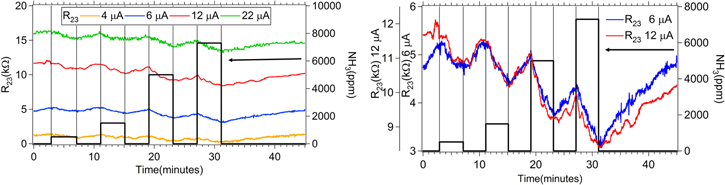
Figure 11. Resistance of a printed GO sensor versus time for four different applied currents as ammonia gas was admitted into the chamber (left). After the exposure to ammonia, the resistance trends upward towards the initial condition. Overlay of the change in resistance of a printed GO sensor exposed to ammonia (right)—electrode 1 current is 6 μA (blue) and 12 μA (red).
Download figure:
Standard image High-resolution image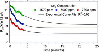
Figure 12. Sensor resistance versus time during the 4 min long exposures to 1500, 5000, and 7300 ppm of NH3 taken from figure 11, right. Exponential curve fits of the data are also included. The data suggest it takes 10–20 min to reach equilibrium.
Download figure:
Standard image High-resolution image
The resistance of the electrospray-printed GO devices decayed with an exponential behavior upon exposure to ammonia during the 4 min doses at different concentrations (figure 12). From the curve fits, the estimated time to equilibrium is 10–20 min, which is much slower than what was observed in the RH experiments. After the exposure to ammonia was completed, the resistance of the device trended back towards the initial value.
There have been reports of the resistance of rGO sensors increasing with increased concentration of NH3 as would be expected for ammonia adsorption onto a GO surface [19, 22, 23], and both increasing and decreasing (anomalous behavior) with increasing NH3 concentration [20]. A simple semi-empirical gas adsorption model has been proposed in the literature to explain the anomalous result observed [20]; the model is based on an existing model for carbon nanotubes. The model proposes that the normalized change in resistance with time is proportional to an offset constant plus an exponential, i.e., R(t)/Ro = A + Be−Ct, where A, B, and C are constants. By selecting appropriate values for A, B, and C, either expected or anomalous behavior for the adsorption and desorption of ammonia onto a GO surface can be fit. It is possible that the GO network of nanoflakes and/or the Au electrodes of the sensors were irreversibly affected by the exposure to amonia, leading to the anomalous behavior [20]. Observation of the device after exposure to ammonia and other reactive gases did exhibit signs of electrode degradation (figure 8). More testing will need to be completed to understand the resistance trends of the devices.
Finally, additive manufacturing could also be used to create at a low-cost, more capable printing hardware; in particular, massively multiplexed arrays of electrospray emitters have recently been demonstrated using stereolithography [34]; these devices could be leveraged to implement a dot matrix printing head similar to the printing head already demonstrated in silicon [13], but at a visibly lower fabrication cost and fabrication time.
Conclusions
Low-cost conductometric gas sensors that use an ultrathin film made of a matrix of GO nanoflakes as transducing element have been reported. The devices were fabricated by lift-off metallization and near-room temperature, atmospheric pressure electrospray printing using a shadow mask. The sensors are sensitive to reactive gases at room temperature without requiring any post heat treatment, harsh chemical reduction, or doping with metal nanoparticles. The sensors' response to humidity at atmospheric pressure tracks that of a commercial sensor, and is linear with changes in humidity in the 10%–60% RH range. In addition, the increase in resistance of the GO sensors with increasing RH found in our experiments followed the same behavior observed for reported sensors made with drop-cast graphene thin films, electrosprayed rGO thin films, individual rGO sheets, rGO/polymer nanocomposites, and randomly oriented carbon nanofibers. Moreover, devices with GO layers printed by different deposition recipes yielded nearly identical response characteristics, suggesting that intrinsic properties of the film control the sensing mechanism. Finally, the printed GO devices successfully detected ammonia at concentrations down to 500 ppm (absolute partial pressure of 5 × 10⁻⁴ T) at ∼1 T pressure, room temperature conditions. The sensor technology can be used in a great variety of atmospheric and sub-atmospheric conditions to aid in industrial process control of applications such as air conditioning and sensing of reactive gas species in vacuum lines and abatement systems.
Acknowledgments
The microfabrication of the devices was completed using the facilities at the Microsystems Technology Laboratories of the Massachusetts Institute of Technology. This work was supported by Edwards Vacuum.