

Abstract
Graphene, the thinnest possible anticorrosion and gas-permeation barrier, is poised to transform the protective coatings industry for a variety of surface applications. In this work, we have studied the structural changes of graphene when the underlying copper surface undergoes oxidation upon heating. Single-layer graphene directly grown on a copper surface by chemical vapour deposition was annealed under ambient atmosphere conditions up to 400 °C. The onset temperature of the surface oxidation of copper is found to be higher for graphene-coated foils. Parallel arrays of graphene nanoripples are a ubiquitous feature of pristine graphene on copper, and we demonstrate that these form crucial sites for the onset of the oxidation of copper, particularly for ∼0.3–0.4 μm ripple widths. In these regions, the oxidation proceeds along the length of the nanoripples, resulting in the formation of parallel stripes of oxidized copper regions. We demonstrate from temperature-dependent Raman spectroscopy that the primary defect formation process in graphene involves boundary-type defects rather than vacancy or sp3-type defects. This observation is consistent with a mechanical tearing process that splits graphene into small polycrystalline domains. The size of these is estimated to be sub-50 nm.
Export citation and abstract BibTeX RIS
1. Introduction
Despite being an atomically thin layer, graphene has emerged as a significant candidate for protective coating applications, and several recent studies have shown its ability to protect metals and alloys from corrosion [1–9]. This has important consequences towards minimizing rust-related losses, and these concepts can also be extended to applications such as solar cells, which are prone to degradation under environmental conditions. The advantages of graphene as a protective layer for metals are manifold, since large-area graphene can not only be grown directly on several metal and metal alloy foils but can also be readily transferred to almost any reasonably flat surface using facile transfer techniques. Previous studies have shown that graphene acts as a short-term oxidation prevention material up to 200 °C for durations up to a few hours [1]. However, in the long term spanning a few months, the graphene-coated copper foils get oxidized more when compared to uncoated foils, even at room temperature [2, 3]. It has been argued that a uniform oxide layer forms on the uncoated copper foils at room temperature, which protects them from further oxidation. On the other hand, graphene-coated copper foils promote non-uniform oxidation, resulting in cracks in the oxide layer; this leads to more oxidation in the long-term duration [3]. The modification of the Raman spectra of graphene on copper and its intensity correlation with the oxide peak due to aging was studied recently. The enhancement of Raman peaks of graphene on oxidized copper was noted due to an optical interference effect [10]. While the ability of graphene to act as an anti-corrosion barrier in the short-time duration has been firmly established, the structural and chemical changes happening in the graphene layer itself during the surface oxidation process have not been adequately probed. There is a need to identify general concepts linking the mechanical aspects of graphene to the surface changes of the underlying substrate. It has been demonstrated that strain and local depinning of graphene membranes can be influenced by subtle changes on the underlying substrate due to structural phase transitions of the substrate [11] or change in the aspect ratio of the substrate patterns [12]. Graphene is known for its robust mechanical properties, with a Young's modulus of about ∼1 TPa [13, 14], and theoretical calculations have shown that pristine graphene lattice can withstand very large (up to 20%) uniaxial strain [15]. However, for large-area graphene coatings, the presence of grain boundaries, ripples, wrinkles, vacancies, and other defects offer potential sites where mechanical tearing and gas permeation can happen [16]. The need for simultaneously studying oxidation of the metal substrate as well as the disorder in the graphene film follows from the likelihood that both processes strongly influence each other. The adhesion of graphene film on the substrate, its structural integrity, nature, and density of defects in the graphene lattice can determine the extent of surface oxidation of the substrate, while the oxidation process itself may influence these properties of the graphene layer. A comprehensive understanding of these processes will ultimately enable extension of the range of operation of the graphene protective coatings to higher temperature values or for longer time durations, and it may allow novel industrial applications. In this work, we have investigated the structural and chemical changes in single-layer graphene when the underlying copper substrate undergoes rapid oxidation promoted by heating in ambient atmosphere. To get a complete picture on the surface oxidation as well as the changes in the graphene layer, we have performed detailed temperature-dependent studies and compared the results with that on bare copper foil, as well as with graphene transferred to SiO2 and bare silicon substrates.
2. Experimental setup
Single-layer graphene (SLG) was grown on copper foil (Goodfellow, 99.9%, 25 μm thickness) using methane as a carbon source. The copper foil was loaded in the heating zone of a 1-inch diameter quartz tube. The system was evacuated to ∼.05 mbar pressure. The substrate was annealed under 10 sccm of H2 for 20 min at 1040 °C. The growth was performed under 35 sccm of CH4 for 30 min while maintaining the same H2 flow rate at the same temperature. The sample was then fast-cooled to room temperature, following the growth step. Besides the as-grown samples, the chemical vapour deposited (CVD) graphene was also wet transferred to 285 nm SiO2/Si and to polished-Si substrates. Scanning electron microscopy (SEM) images were acquired using a Raith150 Two electron-beam lithography system, operating at 10 kV acceleration voltage. Raman spectroscopy was performed using a Horiba LabRAM HR-800-UV with a laser wavelength of λ = 632.8 nm. In-situ temperature-dependent Raman spectra were acquired on the same system using a Linkam THMS600 micro thermoelectric cell. Optical images were acquired using the microscope attached to the Raman system.
3. Results and discussion
Graphene-coated copper foils were heated at a rate of 20 °C min−1 under ambient pressure, and optical images were taken during the heating process, as shown in figure 1. The optical image of graphene-coated copper foil surface at room temperature is shown in figure 1(a), showing the grain boundaries of the copper surface. The surface shows no perceptible changes up to 200 °C. At 250 °C, the proliferation of a network of dark lines is optically visualized on the surface (figure 1(b)), and these become very prominent at 300 °C (figure 1(c)). At still higher temperatures (400 °C), seen in figure 1(d), the background colour of the copper substrate is completely changed, suggesting that the surface is substantially oxidized.

Figure 1. Optical image of a graphene-coated copper foil at different temperatures: (a) 30 °C, (b) 250 °C, (c) 300 °C, and (d) 400 °C, measured during in-situ heating of the sample at a rate of 20 °C min−1.
Download figure:
Standard image High-resolution imageTo further understand these surface changes, SEM images were taken at various stages of surface oxidation. For this purpose, ex-situ heating of graphene-coated copper foils was performed in ambient condition for 5 min in the temperature range 30–400 °C, and subsequently the SEM images were recorded, as shown in figure 2 for graphene-coated foils. At room temperature, SLG on copper is visualized in the form of arrays of parallel nanoripples (figure 2(a)). The typical width of a single nanoripple is w ∼ 0.1–0.2 μm, though some nanoripples have widths up to 0.5 μm, while the typical length is a few μm. These nanoripple arrays are known to form during the cool-down process following the CVD-graphene growth due to a thermal expansion mismatch between graphene and copper, as well as the surface-stress anisotropy of copper [17]. The formation of these graphene nanoripples is also known to be dependent on the crystallinity of the copper surface [18]. Since our Cu substrate is polycrystalline in nature, the nanoripple arrays are naturally oriented along different directions. The geometry and profile of these graphene nanoripples has recently been explored within the framework of a 'wrinklon' theory, which has wider applicability for films with thicknesses varying up to seven orders in magnitude [17]. Based on the presence of nanoripple arrays and some associated wrinkled regions, the graphene is found to have nearly complete coverage on the substrate after the growth. After 200 °C heating, distinct regions identifiable as oxidized copper (granular, with a bright contrast in the SEM images) are found to be present along with the intact graphene regions (dark contrast and usually with parallel nanoripple arrays) (figure 2(c)). Interestingly, the SEM images for the 200 °C heated samples reveal the presence of two kinds of parallel stripes at several locations: (A) parallel arrays of granular oxidized copper in bright contrast and (B) parallel arrays of intact graphene nanoripples, identical to those seen in pristine graphene at room temperature. In several instances, the oxidizing stripe of copper is seen to merge clearly with the intact graphene nanoripple. For example, such oxidizing copper stripes can be seen merging with graphene nanoripples of the same widths in regions labelled '5' and '7' in figure 2(c). The parallel oxidized stripes of the copper surface are themselves separated by a thin intervening region where the graphene is likely intact, and, therefore, the oxidation is curtailed. Such regions could represent locations where graphene nanoripples strongly adhere to copper in the form of troughs of the oscillating nanoripple array (see schematic in figure 3(a)). These observations strongly suggest that the intervening spatial regions between the graphene nanoripples and the underlying substrate are crucial sites for the onset of copper oxidation, and, further, the oxidation likely proceeds along the length of the graphene ripple, which is destroyed in the process. Another notable feature is that of regions lacking any nanoripples (such as the region labelled '8' in figure 2(c)); these remain un-oxidized, and, further, the regions with closely spaced graphene nanoripples also appear to lack this initial oxidation. This naturally brings us to the question of whether any nanoripple size favours oxidation. To examine this possibility, we have considered the statistics of the state of oxidation measured across 50 such graphene nanoripples or oxidized copper nanostripes for the 200 °C heated sample in figure 3(b). A band of widths ranging about ∼0.3–0.4 μm is seen to be preferentially oxidized. Similar results are obtained from other regions at 200 °C. At 300 °C (figure 2(d)), the surface is substantially covered with copper oxide grains, while islands of apparently intact graphene of size ∼1 μm can still be resolved. At 400 °C, the surface looks completely oxidized, but a few well-separated and smaller graphene islands are still present, as shown in figure 2(e). These graphene regions that appear to best withstand oxidation are free of nanoripples—which once again points to the important role of nanoripples in the oxidation process. Lastly, we note that in addition to the oxidized nanostripe arrays, some adjacent granular regions with bright contrast, but lacking any nanostripe features, can also be seen (such as between regions '2' and '6' in figure 2(c)). For these regions, it is plausible that oxidized nanostripe features were formed during some early stage of annealing, but these features subsequently got obliterated when the oxidation process advanced further. A different possibility is that these were the regions where microcracks and tears had formed on the graphene layer during or before the annealing step, and, consequently, the copper was preferentially oxidized there.
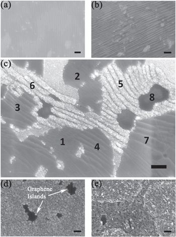
Figure 2. SEM images of graphene-coated copper foil subsequent to heat treatment at different temperatures: (a) room temperature, (b) 100 °C, (c) 200 °C (The numbers 1–8 denote regions with different widths of graphene nanoripple arrays or of oxidized copper nanostripe arrays), (d) 300 °C, and (e) 400 °C. Scale bar is 1 μm for all images.
Download figure:
Standard image High-resolution image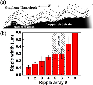
Figure 3. (a) Schematic of oxidation of copper below graphene nanoripples of width W. (b) Bar plot showing preferential oxidation of certain widths of graphene nanoripples. Ripple array number corresponds to regions marked in figure 2(c).
Download figure:
Standard image High-resolution imageThe surface oxidation processes noted above are further explored using in-situ temperature-dependent Raman spectroscopy. The data was acquired with a 50X objective while a heating rate of 20 °C min−1 was maintained under ambient pressure. The spectra were recorded after a 1 min delay subsequent to reaching the set temperature. Figure 4(a) shows the temperature-dependant Raman spectra of graphene-coated copper foil, and figure 4(b) is the corresponding temperature-dependent Raman spectra of bare copper foil in the interval 175–425 cm−1 taken at the same location shown in figure 1. Copper forms mainly two types of oxides: CuO and Cu2O, which can be identified with the Raman mode frequencies [1, 19, 20]. In this work, we mainly use the mode at about 290 cm−1 for identifying the presence of CuO and the mode at about 220 cm−1 for Cu2O. We first discuss the as-purchased bare foil, which shows a very small copper oxide peak at room temperature that remains unchanged up to 150 °C. At 200 °C, the Cu2O peak starts appearing, and its intensity increases with temperature. Above 350 °C, the CuO peak also appears. Previous studies on the oxidation of a bare copper surface have shown that the surface at ambient temperature is covered with a Cu2O layer with a small CuO layer on the outer surface, and the layer thickness increases with temperature [21–23]. Similar changes representing the oxidation of the surface of copper are observed for the case of graphene-coated copper foil. Based on the Raman spectrum, no copper-oxide Raman peaks are visible in as-grown graphene-coated copper foil up to 200 °C. Notably, the temperature onset of oxidation for the graphene-coated copper surface is higher (T = 250 °C) when compared to that of the bare copper foil (T = 200 °C), with both foils heated under an identical ramp rate. This is in agreement with previous studies that have reported the corrosion-prevention properties of graphene in the short run [1, 3]. Graphene may act as a diffusion barrier to oxygen, and oxygen can only reach the copper surface through the defects, grain boundaries, and cracks of graphene film, since pristine graphene is impermeable to gases, whereas uncoated copper foil has a uniform exposure to atmospheric oxygen. Our data suggests that under conditions of rapid heating (∼10 min), graphene-coated surfaces are less oxidized at a given temperature.

Figure 4. Temperature-dependent Raman spectra showing evolution of copper oxide peaks for (a) graphene-coated copper foil and (b) bare copper foil.
Download figure:
Standard image High-resolution imageWe next examine to what extent graphene remains chemically intact during the surface oxidation process of copper. The temperature-dependent Raman spectra of CVD graphene wet-transferred to 285 nm thermal SiO2/Si and of graphene grown on copper foil are shown in figures 5(a) and (b), respectively. We first discuss the data for graphene on a SiO2 substrate obtained while heating this sample at 20 °C min−1. The three main Raman peaks of graphene are a D, G, and 2D peak, centred about 1330, 1580, and 2630 cm−1, respectively. The G and 2D peaks originate from optical phonon modes of pristine graphene, while the D peak is related to the presence of defects [24]. Our high-quality samples show a negligible defect peak at room temperature. The temperature-dependent Raman data for the graphene:SiO2 system unambiguously shows that the small D peak's intensity remains nearly unchanged in the temperature interval 30–400 °C. This indicates that graphene is inherently chemically inert when subject to air heating. The positions of the G and 2D peaks vary with temperature; these aspects are discussed in more detail below. In contrast to the data for the graphene:SiO2 system, the graphene:copper system shows significant changes in the temperature-dependent Raman data, as plotted in figure 5(b). In particular, the widths of the 2D and G peaks are significantly broadened at 300 °C, while the evolution of a broad D peak can also be seen. The explanation of the above observations is related to the formation of defects in the graphene lattice, though the nature of the defects and the defect density need to be quantified (as discussed later in the text). To analyze the data further, a plot of full-width-at-half-maxima (FWHM) of the G peak versus temperature is shown in figure 5(c) for the graphene on copper and SiO2 substrates. On the SiO2 substrate, the G peak width is nearly independent of temperature up to 400 °C, and its value of 16–19 cm−1 is consistent with the values expected for pristine SLG with a Fermi level close to the neutrality point [25]. In contrast, for graphene grown on copper, the FWHM starts to increase from 150 °C, and at 250 °C there is a sharp increase to large values ∼52 cm−1. While small variations of the G peak width can normally be accounted with a change in Fermi level, such a large FWHM width is not representative of pristine graphene. Instead it represents the formation of defects on the graphene lattice or the formation of amorphous carbon alongside graphene [26]. Figure 5(d) is the plot of the G peak position of graphene on copper and SiO2 substrates as a function of temperature. As temperature increases, the G peak position shows a monotonic decrease on SiO2, which can be explained, due to lattice strain, as a consequence of a thermal expansion mismatch with the substrate, along with the anharmonic contribution and thermal expansion of the graphene lattice itself [27]. The estimated shift in the G peak with temperature, ΔωG(T) = 0.022 cm−1 K−1, is in agreement with the value obtained from thermal mismatch strain studies (0.024 cm−1 K−1) for the graphene:SiO2 system [28]. A similar trend happens on the copper substrate as well, but the change is significantly more rapid, as seen from the slope of the plot in figure 5(d) for T ≤ 200 °C. Since our Raman study indicates that oxidation of the substrate does not commence until 200 °C, the decrease in the G-peak position can entirely be attributed to the three thermal expansion-related effects, already noted above. For graphene on copper foil, this trend of decrease in ωG(T) with an increase in temperature is reversed after 200 °C. This reversal can be attributed to loss of lattice strain, such as that which may arise from cracks or tearing of graphene. This may appear rather surprising, since graphene should withstand up to 20% lattice strain before bond breakage [15], while the strain change estimated from the G-peak shift is rather small—less than 0.5%. The likely sites for fracture may therefore lie in grain boundaries or other line defects. For temperatures between 200–400 °C, ωG(T) increases and approaches high values of ∼1592 cm−1; this large upshift can be explained due to the formation of defects, which will upshift the G peak [29].
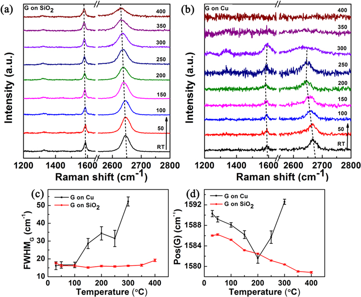
Figure 5. (a) Temperature-dependent Raman shift of graphene on a SiO2 substrate. (b) Temperature-dependent Raman shift of graphene on copper foil. (c) Comparison of FWHM of graphene G-peak on copper and on SiO2 at different temperatures. (d) Comparison of G-peak position of graphene on copper and SiO2 at different temperatures.
Download figure:
Standard image High-resolution imageWe next discuss the Raman spectrum of graphene transferred to the SiO2 substrate subsequent to heating on the copper foil. Graphene-coated copper foils were heated for 5 min on a hot plate at different temperatures, and, following that, the graphene was transferred to SiO2. The advantage of examining the samples on 285 nm SiO2/Si arises from the high optical contrast difference between graphene and the SiO2 substrate, which allows easy identification of graphene regions [30]. Graphene films were seen to be continuous up to 100 °C heating under optical microscope, but they appear to progressively tear above 200 °C. Figure 6(a) is a typical Raman spectrum of graphene transferred to a SiO2 substrate subsequent to 350 °C heating on a copper substrate. The spectrum shows all the major Raman peaks associated with defected graphene: D, D', D'', D + D', D + D'', and 2D', besides the G and 2D peaks [24]. Figure 6(b) shows the Raman spectra of the above graphene for different heating temperatures. The most important changes are with respect to the defect peak. A small D peak is sometimes observed in our unheated graphene samples, and similar spectra are observed for the 100 °C heated sample. These can be attributed to edges and sub-domain grain boundaries of CVD graphene formed during the growth process [31]. From 200 °C onwards, the D peak continuously increases in intensity. In addition to the D peak, the D' peak of about 1620 cm−1 starts originating at 200 °C, and its intensity also increases with temperature. The D' peak originates from the double resonance occurring at the same Dirac cone and is also characteristic of defected graphene samples [24]. Figure 6(c) shows the FWHM of the G and 2D modes as a function of temperature. The FWHM shows small variations up to 200 °C, and, subsequently, there is significant broadening, which is attributable to defect formation, as also discussed above [29]. Figure 6(d) is a plot of the integrated intensity ratio of D with G, ID/IG, with heating temperature. The evolution of the Raman spectra of defected graphene has previously been considered in a three-stage model [26] involving changes from graphitic to nanocrystalline forms and, further, to amorphous and tetrahedral amorphous forms. For the range of variation of ID/IG in our work, the transition is primarily from graphene to the nanocrystalline graphene type. The ID/IG for this stage scales inversely with crystallite size, La [32]. The value of La is obtained from the equation,  where λl is the laser wavelength in nm [32], and the corresponding plot of La versus temperature is shown in figure 6(d). The reduction in crystallite size can be attributed to the mechanical tearing of graphene, and above 250 °C, the crystallite size reduces below ∼50 nm. This length scale compares well with the individual grain size of oxidized copper, and the tearing of graphene may happen at the individual grains of oxidizing copper. Finally, we considered the extent of defect formation for graphene transferred to mildly oxidizing substrates such as cleaned and polished Si and heated under the same conditions (figure 6(e)). In this case, the extent of defect formation is significantly lower when compared to that of graphene on copper. Therefore the depth of oxidation of the substrate and the associated roughness and granularity may play a major role in determining the tearing process.
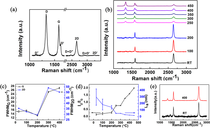
Figure 6. (a) Raman spectrum of graphene transferred to SiO2 substrate subsequent to 350 °C heating on copper substrate. (b) Raman spectra of graphene transferred to SiO2 subsequent to heating on the copper substrate at different temperatures. (The spectra are normalized for G-peak intensity.) (c) FWHM of graphene G and 2D peak versus temperature. (d) Intensity ratio ID/IG versus temperature. (e) Raman spectra of graphene transferred and heated on cleaned and polished Si surface at room temperature and after 400 °C heating.
Download figure:
Standard image High-resolution imageIn the estimation of La, we assumed that crystallite size was primarily responsible for defects. This assumption can be validated by a comparison of the evolution of D and D' peaks. In the work of Eckmann et al graphene was subjected to gas plasmas of different compositions, resulting in the formation of different types of defects, including sp3-bonded defects in hydrogenated and fluorinated graphene and vacancies due to ion bombardment [33]. The comparative evolution of the peak intensities of the D and D' modes has been used as an empirical indicator of the type of disorder in the system [33]. Figure 7 is a plot of ID'/IG versus ID/IG. The slope of the data in this graph is about 3.8 ± 0.2. For comparison, the slope of ID'/IG versus ID/IG for vacancy-type defects is about 7, and for an sp3-like defect it is about 13, while that for boundary-type defects is ∼3.5 [33]. The slope value obtained for our samples clearly corresponds to boundary-like defects, which are normally present in polycrystalline graphene. This comparison indicates that the nature of defects created by heating graphene on copper is boundary-like; i.e., graphene is fractured in domains when the underlying substrate gets oxidized during the heating. At the same time, the formation of localized defects like vacancies or sp3 may not be significant.

Figure 7. Plot of ID/IG versus ID'/IG plotted together with literature values of the slopes for different types of defects. Red circles indicate data from our samples.
Download figure:
Standard image High-resolution image
4. Conclusion
In conclusion, we have studied the progressive mechanical tearing of SLG on an annealed copper substrate undergoing oxidation. While graphene delays the temperature onset of oxidation under rapid oxidation conditions, it itself undergoes temperature-dependent mechanical tearing. Our detailed Raman spectroscopy analysis confirms that mechanical tearing of graphene into polycrystalline domains of sub-50 nm size constitutes the predominant defect generation mechanism in graphene during this surface oxidation process. The onset of copper oxidation at 200 °C is characterized by the formation of parallel stripes of oxidized regions, and we have attributed the formation of these structures to the oxidation of copper underneath parallel arrays of graphene nanoripples. We suggest that one key to achieving better graphene-based protective coatings in future may lie in restricting the formation of nanoripple arrays or engineering their geometry. This, together with the growth of large- domain graphene, may help to realize the true potential of these atomically thin membranes for surface protection applications.
Acknowledgments
MJ thanks financial support from DST-SERB Grant No. FTP/PS-072/2012, DAE YSRA Grant No. 2012/20/37P/10/BRNS, Nissan NRSP, and IIT-M NFSC. AG thanks IIT-Madras for financial support. The authors gratefully acknowledge the use of facilities at the Centre for NEMS and Nanophotonics, funded by DeitY.