

Abstract
Cylindrical Fe28Co67Cu5 nanowires modulated in diameter between 22 and 35 nm are synthesized by electroplating into the nanopores of alumina membranes. High-sensitivity MFM imaging (with a detection noise of 1 μN m−1) reveals the presence of single-domain structures in remanence with strong contrast at the ends of the nanowires, as well as at the transition regions where the diameter is modulated. Micromagnetic simulations suggest that curling of the magnetization takes place at these transition sites, extending over 10–20 nm and giving rise to stray fields measurable with our MFM. An additional weaker contrast is imaged, which is interpreted to arise from inhomogeneities in the nanowire diameter.
Export citation and abstract BibTeX RIS
1. Introduction
The determination of the spin configuration of nanoscale magnetic systems and the control over their magnetization reversal process is essential for progress in advanced information storage, logic systems, biomedical applications, clean energy sources and sensing devices [1–4]. Controlled displacement of magnetic domain walls (DWs) along ferromagnetic nanowires by means of electric currents [1, 5] or magnetic field pulses [6] has recently advanced to become one of the most intensively studied topics in magnetism [7]. In planar nanostrips fabricated by nanolithography, DWs are artificially pinned by notches or local stray fields [8] but less attention was paid to cylindrical nanowires (NWs) until the discovery of the new opportunities they offer to control the shape and dynamics of the DWs for spintronic application [9]. Cylindrical NWs are currently synthesized by electroplating into nanopores [10] with the possibility to modulate their diameter [11], inducing local pinning centers that tailor the reversal mechanism [12]. On the other hand, concerns about resource scarcity and the search for renewable and clean energy sources have led to novel families of permanent magnets. In particular, CoFe-based NWs are among the most optimal candidates because they exhibit high saturation magnetization and good thermal stability [10].
The objective of this work is twofold. A first achievement is the fabrication of modulated NWs with smaller diameters than previously reported (down to 22 nm). In addition, the resulting spin configuration in individual NWs has been imaged and correlated to their morphologies. Note that few experimental techniques allow for direct imaging of spin configurations in this kind of nanostructure; among them, magnetic force microscopy (MFM) is currently the most widespread and accessible one for this purpose [13–15].
2. Methods
Fe28Co67Cu5 NWs were grown by electrodeposition onto the pores of anodic aluminum oxide (AAO) membranes [16], obtained after a two-step anodization process [17] (figure 1). The geometry of the nanochannels is controlled not only by the anodization time, voltage or bath temperature but also by the shape of the pulses in the second anodization step. The resulting cylindrical modulated pores are formed by segments with diameters of around 22 and 35 nm, while the center-to-center inter-wire distance is kept constant at 65 nm [11]. NWs were subsequently grown into the modulated pores by electrodeposition from a sulfate-based electrolyte [17], with a final length of around 7 μm.
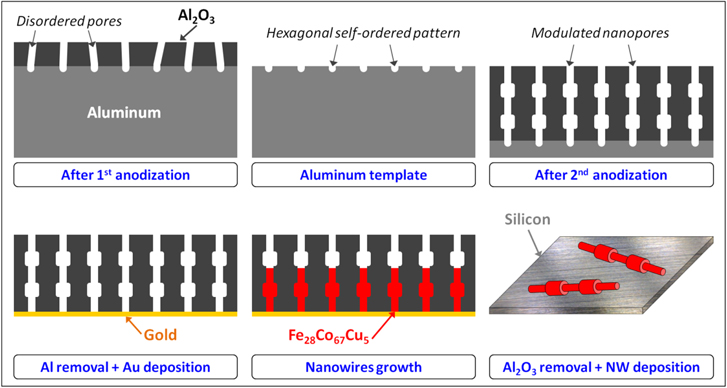
Figure 1. The fabrication process. Schematics of the main steps followed during the fabrication of the FeCoCu nanowires and the preparation for the subsequent MFM experiments.
Download figure:
Standard image High-resolution imageAluminum foils (99.999%; Goodfellow) are electropolished in a mixture 1:4 of HClO4:C2H5OH at 20 V under vigorous stirring. Aluminum foils are anodized in sulfuric acid–based electrolyte with 3 wt% concentration. The anodization process is performed within a Teflon electrochemical cell refrigerated at the base and the walls, so that both the aluminum foil and the electrolyte are directly cooled. This system provides high thermal stability at 0 °C during the processes. Prior to the pulsed anodization process, a nanopatterned aluminum foil is obtained after removal of the AAO resulting from 16 h of a conventional first anodization at 25 V (figure 1). In order to improve the mechanical stability and avoid the breakdown of the anodized film during the first hard anodization (HA) pulse, the duration of the first mild anodization (MA) pulse was extended to 15 min, followed by alternating MA and HA pulses. The sequence of the anodization pulses applied during the process is 150 s for MA segments and 200 ms for HA segments, repeated 10 times. The resulting length of the nanochannels is about 40 μm. The resulting cylindrical modulated pores are formed by segments with diameters of 22 and 35 nm for MA and HA respectively, while the center-to-center inter-pore distance (within the membrane) is kept constant at 65 nm. After the anodization process, the aluminum substrate is removed with an aqueous solution composed of copper chloride and hydrochloric acid and the alumina barrier layer is etched with an aqueous solution of H3PO4, 5 wt%. A gold layer is sputtered onto one side of the alumina template to ensure the good conductivity needed for electrochemical deposition.
Cylindrical Fe28Co67Cu5 nanowires around 7 μm in length were subsequently electroplated into the cylindrical modulated pores by electrodeposition from a sulfate-based electrolyte containing CoSO4 · 7H2O (35 g l−1), CuSO4 · 5H2O (2 g l−1), FeSO4 · 7H2O (15 g l−1), H3BO3 (10 g l−1) and ascorbic acid (10 g l−1). The resulting nanowires were then periodically modulated in diameter between 22 and 35 nm. The electrochemical deposition was carried out under potentiostatic conditions by applying −1.8 V to a Ag/AgCl reference electrode, keeping the temperature of the electrolyte at 25 °C and the pH value at about 3.0. As a result, a macroscopic membrane enclosing a very large number of ferromagnetic nanowires is obtained. The alloy composition of the electrodeposited samples was identified by means of energy dispersive x-ray spectroscopy (EDS). The membrane was then divided into different pieces so that bulk magnetometry measurements were performed, on the one hand, whereas dissolution of the alumina and subsequent deposition onto a Si substrate (figure 1) was followed up by TEM and MFM analysis of single Fe28Co67Cu5 elements, on the other hand.
3. Results and discussion
Hysteresis loops were obtained at RT with the NWs inside the membrane by means of vibrating sample magnetometry (VSM), with a maximum magnetic field of ±1.7 T applied either along the longitudinal or transverse directions. Analysis of the longitudinal loop (figure 2(a)) suggests the existence of relatively large magnetostatic interactions between neighboring elements, as expected from the small inter-pore distance [18]. As a result, reduced values for the susceptibility and remanent magnetization (about 41% of the saturation value) are obtained.
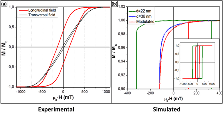
Figure 2. (a) Hysteresis loops of NWs embedded within the membrane. (b) Simulated loops of individual NWs with either constant (d = 22 nm or 36 nm) or modulated diameters (dmin = 22 nm and dmax = 36 nm).
Download figure:
Standard image High-resolution imageUpon dissolution of the AAO membrane, high-resolution transmission electron microscopy (HR-TEM) characterization was performed to evaluate the crystallinity and the structural properties of the NWs [19]. Figure 3(a) shows the modulation in diameter of a single NW, with magnified images of segments about 35 nm and 22 nm in diameter presented in figures 2(b) and (c), respectively. The mean segment length of constant diameter was found to be 500–600 nm. Regarding crystallinity, the nanostructures present a bcc crystalline structure with the wider parts being highly textured along the [110] direction, whereas the narrow segments show weaker texture. A surface amorphous layer with a thickness of 2–3 nm is observed throughout the NW length, in agreement with previous studies [20] on uniform FeCoCu NWs, and originated by the mismatch between the NW crystalline structure and the alumina during the growth process. A small surface roughness of a few nm is observed at both interfaces of the amorphous layer; its effect on the magnetic properties will be analyzed and recalled later.

Figure 3. HR-TEM images of a modulated NW, where (a) a modulation in the diameter is clearly observed. (b) Area highlighted with a red square in (a), showing a bcc high textured region along the [110] direction. (c) Area framed in blue in (a), revealing a weaker texture.
Download figure:
Standard image High-resolution imageIn order to gain information about the magnetic behavior of individual NWs, MFM imaging was performed with a Nanotec Electrónica system making use of the amplitude modulation (AM) and two-pass modes; in addition, a phase-locked loop (PLL) was enabled to track the resonance frequency of the oscillating cantilever (k ≈ 3 N m−1, f0 ≈ 75 kHz). The existence of eventual artifacts generated by the overlap of electrostatic interactions [21] can be ruled out, as deduced from Kelvin probe force microscopy experiments (not shown); similarly, effects associated with irreversible tip-sample influence [22] were not relevant. MFM was implemented at low scan speed, allowing the lock-in amplifier to filter out the majority of noise sources and yielding high resolution [23] and enhanced signal-to-noise ratio with a frequency shift noise level of 20 mHz. This value corresponds, assuming a point-mass model and the harmonic approximation, to a force gradient detection limit of only 1 μN m−1 in ambient conditions.
Figures 4(a) and (b) show the topography and its corresponding MFM image of several modulated NWs in their remanent state. Similar MFM images showing the as-grown and demagnetized states can be found in the supplementary information (SI.1). The interpretation of the MFM image is rather difficult since several series of spots with relatively strong contrast are found at different positions along the wires. At first sight, this suggests the existence of complex configurations involving several DWs as every NW displays a number of attractively and repulsively interacting regions (dark and bright contrast, respectively). A deeper insight into the underlying configurations can be obtained with the help of micromagnetic simulations. These were performed using an object oriented micromagnetic framework (OOMMF) to simulate the magnetic behavior of individual NWs. A (2 × 2 × 2) nm3 cubic cell size was considered, with a saturation magnetization MS = 1.59 · 106 A m−1 and exchange stiffness A = 10.7 · 10−12 J m−1. As previously reported [24], the weak magnetocrystalline anisotropy was assumed not to play a significant role.

Figure 4. (a) Topographic and (b) MFM images (25 × 25) μm2 in size of modulated NWs in remanence deposited onto a Si substrate.
Download figure:
Standard image High-resolution imageSimulated hysteresis loops are shown in figure 2(b) for the case of a longitudinal field applied to three different NWs (2 μm in length) simulated independently. Two of them were designed with a uniform diameter of 22 nm (narrow) and 36 nm (wide), the third one having a modulated diameter with two narrow and two wide segments (500 nm long; see figure 5(c)). For each simulation, the initial distribution of the magnetization was set to be oriented along the main axis of the NW (initial saturated state) and its evolution with an external field was studied in the range (1 T, −1 T), including a step at zero field (remanent state). Additionally (refer to the supplementary information (SI) available at stacks.iop.org/NANO/26/395702/mmedia), the demagnetized state was simulated by starting from a randomly oriented distribution of spins and studying its evolution without the presence of any external field (SI.1), revealing the formation of transversal domain walls during the process (shown in SI.2).

Figure 5. (a) Topography and (b) MFM images (2.7 × 0.4 μm) of a single NW in remanence. (c) Simulated configuration for a modulated NW equivalent to the experimental case. A single domain state is obtained with large divergence of the magnetization at the discontinuities. The black–white scale stands for a negative–positive divergence of the magnetization, analogous to the MFM case. (d) Zoom-in on the region framed in blue in (c). (e) Cross section view of the area enclosed by the dashed square line in (d).
Download figure:
Standard image High-resolution image
For each of the three simulated NWs, square hysteresis loops were obtained with remanent magnetizations up to 98% of the saturation value (inset in figure 2(b)), as expected from single-domain wires [24]. The reversal process in uniform wires is mediated by two vortex walls nucleating at both ends and propagating inwards [26], this propagation taking place at lower field values in the case of wide NWs. In the same manner, reversal in the modulated NW is triggered by the vortex wall nucleated in the wider segment, which explains the similarities of the hysteresis loops between the modulated and 36 nm uniform wires (figure 2(b)). The slightly lower value of the magnetization observed in the modulated structure right before the Barkhausen jump is associated with magnetization curling taking place at the discontinuities [27]. For these small transverse dimensions, Bloch-point DWs are not expected to be energetically favorable [9, 28].
Comparison with the experiment can be made by considering an individual NW as the one shown in figure 5. In the MFM image (figure 5(b)), two types of magnetic contrast can be identified: (i) relatively intense spots not only present at the ends of the wires but also at specific positions along the nanostructures, and (ii) a weaker alternating contrast observed all along the element.
The topographic profile of the NW has been highlighted by white dashed lines in figures 5(a)–(b) to help correlate the magnetic contrast with the morphology. From there, one can readily identify the strong contrast to be originated at discontinuities in the diameter, in excellent agreement with the simulated MFM image depicted in figure 5(c). Zooming into a transition region between segments (figure 5(d)) reveals that the orientation of the magnetization in remanence is essentially oriented along the longitudinal axis of the NWs. Therefore, the origin of the strong divergence is purely shape-induced at the modulation sites with the aim to minimize the magnetostatic energy. As a result, magnetization curling takes place (figure 5(e)) in narrow regions that extend over 10–20 nm into the wider segments of the NW. These transition regions might eventually be used to modify the speed of a propagating DWs in this kind of nanostructure [29, 30]. More examples of single NWs showing more complex configurations in demagnetized states, including DWs determined to be transverse-like by simulations, are analyzed in SI.2.
In addition, weak alternating spots not predicted by simulations are present along the NW (figure 5(b)). This contrast becomes noticeable due to the enhanced resolution and sensitivity of the MFM data shown in this work. Analogously to the former case, a general correlation can be identified between subtle topographic protuberances and the weak contrast in the MFM signal. As was previously mentioned in the HR-TEM analysis (figure 3), the outermost layers of the NWs present a corrugation on the order of few nm; therefore, we attribute this quasi-periodic weak contrast to morphological deviations from a smooth cylindrical surface. Further information on this can be found in SI.3, where MFM data on straight NWs of the same composition but constant diameter are presented, displaying single-domain behavior characterized by strong contrast at the ends and a similar series of weak spots. These results should encourage MFM users to be particularly careful with the interpretation of data in this kind of sample as similar effects should be observed in narrow nanostrips or NWs if substantial corrugation and enough sensitivity is reached during the measurement [31, 32].
4. Conclusions
This work presents the fabrication of cylindrical Fe28Co67Cu5 NWs with modulated diameter segments as thin as 22 and 35 nm. The effect those modulations have on the spin orientation has been unveiled by high-sensitivity MFM imaging and supported by micromagnetic simulations. The complex contrast in the resulting images requires a careful non-trivial interpretation that suggests the single-domain state is favorable in remanence, with a curling of the magnetization at the transition regions between segments of different diameter. In addition, a weaker contrast was correlated to a surface corrugation of few nm caused by the mismatch of the crystalline structure of the NWs and the AAO nanopores.
Acknowledgments
The authors acknowledge support from the Spanish MINECO under projects CSD2010-00024 and MAT2013-48054-C2-1-R and from the EU commission under project 'REFREEPERMAG' FP7NMP.2011.2.2.
Supporting information
- MFM images of Fe28Co67Cu5 NWs in the as grown and demagnetized states.
- Domain walls in demagnetized individual NWs.
- MFM images of non-modulated Fe28Co67Cu5 NWs.