

Abstract
Luminescence of p-type GaAs was induced by electron injection from the tip of a scanning tunnelling microscope into a GaAs(110) surface. Atomically-resolved photon maps revealed a significant reduction in luminescence intensity at surface electronic states localized near Ga atoms. Theoretical analysis based on first principles calculations and a rate equation approach was performed to describe the perspective of electron energy dissipation at the surface. Our study reveals that non-radiative recombination through the surface states (SS) is a dominant process for the electron energy dissipation at the surface, which is suggestive of the fast scattering of injected electrons into the SS.
Export citation and abstract BibTeX RIS
1. Introduction
The energy dissipation of electrons, such as recombination and scattering, plays a significant role in current electronic technologies. In particular, recombination at surfaces is one of the principal processes responsible for reducing the operational efficiency of (opto)electronic devices and (photo)catalytic systems [1, 2]. The recent development of various nano-materials further raises the importance of precisely understanding recombination at surfaces because such materials have large surface-to-volume ratios [1–3]. However, thus far, it has not been feasible to obtain quantitative information about surface recombination at the atomic-scale, mainly because of technical limitations.
The investigation of surface recombination requires the selective excitation of surface electronic states. In cathodoluminescence (CL) and photoluminescence (PL), which have been widely used to study recombination processes in semiconductor materials [4], electronic excitation occurs mainly inside the bulk, which hampers investigation of surface phenomena. Two-photon photoemission (2PPE) has been applied to the study of electron dynamics at various semiconductor surfaces [5–8], but 2PPE is not capable of obtaining detailed spatial information. In contrast, scanning tunnelling luminescence (STL) [9–12], where luminescence is induced by electron tunnelling from the tip of a scanning tunnelling microscope (STM), has several distinctive capabilities. Selective and direct excitation of surfaces can be achieved by the injection of energetic electrons into surface electronic states in STL. Additionally, the ability of STL to spatially resolve materials at atomic resolution makes it unique among optical techniques. In conjunction with morphological observation with an STM and electronic state measurement using scanning tunnelling spectroscopy (STS), STL is an ideal tool for investigating surface recombination.
GaAs, a III–V compound semiconductor, is one of the most important industrial materials used in optoelectronic devices such as photovoltaic cells and lasers. The electronic properties of the GaAs(110) surface have been extensively studied using photo-electron spectroscopy [5, 6], theoretical calculations [13–15], and STM [14–24]. GaAs(110) has also been studied with STL with the focus primarily on understanding the mechanism of luminescence induced by STM, including electron tunnelling, electronic transitions, and electromagnetic enhancement [9, 25–29]. However, STL has never been used to investigate the surface recombination at a GaAs(110) surface, and so far detailed features of electron energy dissipation at the surface have not been reported.
In this paper, we report a perspective of electron energy dissipation at a p-type GaAs(110) surface investigated by STL spectroscopy and theoretical analysis. Measurement of STM topography, STS map and STL photon map with atomic spatial resolution revealed apparent reduction in luminescence intensity at the surface states (SS) localized near Ga atoms. The experimental data were theoretically analyzed using both first principles calculations and a rate equation approach, and the reduced photon yield in STL is interpreted in terms of the probability of electron injection into the SS as well as electron scattering and non-radiative recombination at the surface.
2. Method
Experiments were performed with a low-temperature STM (Oxford Instruments) operating at 4.7 K under ultrahigh vacuum (UHV). The STM stage was modified to be equipped with two optical lenses (each covers a solid angle of 0.5 Sr). The emitted light was collimated and led outside the UHV chamber with a lens and refocused into a spectrometer (Acton, SpectraPro 2300i) with a liquid N2 cooled charge coupled device photon detector (Princeton, Spec10-100B-eX). All the optical spectra were measured using a grating with 300 gr/mm and the spectral resolution of the optical system in wavelength was better than 1 nm, which corresponds to an energy resolution better than 0.003 eV at 1.5 eV. In the STL measurement, except for the luminescence spectrum, integrated photon intensity over a wavelength range 750–1000 nm was plotted. The sample was p-type GaAs which was heavily doped with Zn at a carrier concentration of around 2 × 1019 cm−3 and cleaved under UHV to expose clean (110) surfaces. The STM tip was prepared by electrochemical etching of a tungsten wire.
First principles calculations based on density functional theory (DFT) were performed to analyze the electronic structure of the GaAs(110) surface. We employed the local density approximation [30] implemented in the Vienna ab initio simulation package code [31, 32]. The core electrons were replaced by projector augmented wave pseudopotentials and expanded in a plan-wave basis set (480 eV cut off) [33, 34]. The repeated slab model consists of 17 atomic (110) planes separated by a vacuum region of more than 15 Å, in which bottom atoms were terminated with hydrogen. Dipole correction was applied in order to avoid artificial interactions between periodic slab images. During ionic relaxations, the two bottom atomic (110) planes were fixed in their bulk positions. Ionic relaxations were performed until atomic forces became less than 0.01 eV Å−1. A 12 × 16 × 1 Γ-centred k-point grid was used for Brillouin zone sampling.
3. Results and discussion
In the STL experiments, the luminescence of p-type GaAs induced by the STM was measured and correlated with the local atomic and electronic structures (figure 1(a)). Figure 1(b) shows the STL spectra of the GaAs(110) measured at various sample voltages (V) and a PL spectrum as a reference. Luminescence in STL was observed only at positive V when  was less than 2 V [25]. The shape of the STL spectra (a single peak at 1.47 eV and a cut off at 1.51 eV) did not depend on V, and it was almost identical to that of the PL spectrum, suggesting that no radiative recombination occurs at the surface. The absence of radiative recombination from the SS is consistent with the characteristic band structure of the surface with a conduction band (CB) minimum at the X-point [5, 13], which will be described later with the results of the DFT calculations. Because the excitation light in PL penetrates about 100 nm into GaAs [35], the luminescence occurs mainly inside the bulk. Therefore, we concluded that STL also occurs inside the bulk.

Figure 1. Luminescence and electronic properties of GaAs(110) and a proposed process. (a) A schematic drawing of STL measurement of p-doped GaAs. Luminescence inside the bulk is induced by electron injection with an STM tip. (b) STL spectra at various voltages and PL spectrum measured on the same sample. All STL spectra were acquired with a tunnelling current (It) of 100 pA and an exposure time of 1 min, with the intensity measured in counts per second (cps). The PL spectrum is normalized and offset. The PL excitation source was a green laser (532 nm, 1 mW). (c) Schematic energy diagram illustrating the proposed process where EF is the Fermi level, P is the non-radiative recombination probability from the surface states (SS) to the acceptor band (AB). Here we consider only non-radiative recombination from the SS based on the fact that no radiative recombination from the surface states was observed in the STL spectra (b). (d) dI/dV curve acquired on GaAs(110) using a standard lock-in technique with a bias modulation of 14 mV. The region near the VB maximum is shown in the inset. (e) Sample voltage dependence of the photon yield. Photon yield = (number of emitted photons)/(number of injected electrons).
Download figure:
Standard image High-resolution imageA proposed process of STL is summarized in figure 1(c). First, electrons tunnel from the tip into SS or the bulk CB. While the electrons are in SS, they may undergo surface non-radiative recombination with a certain probability P. Electrons that do not undergo the non-radiative recombination at the surface penetrate into the bulk CB, followed by thermalization to the CB minimum. They then recombine with holes in the acceptor band (AB) just above the Fermi level, giving rise to luminescence [4, 26]. The abrupt cutoff observed at 1.51 eV in the spectrum suggests that the highest-energy transition is from the CB minimum to the Fermi level, which indicates that the AB merges with the intrinsic valence band (VB) [4, 36]. Figure 1(d), which shows the density of states of GaAs(110) measured with STS, confirms the existence of empty states associated with the AB (indicated by an arrow in the inset of figure 1(d)) [37].
The dependence of photon yield on sample voltage is shown in figure 1(e). The yield exhibits a rapid rise at 1.51 V, and the slope starts to decrease at 1.6 V, followed by saturation at around 1.8 V. This behaviour reflects the ratio of the number of electrons injected into the bulk CB to the total number of tunnelling electrons. When the sample voltage is lower than 1.51 V, the only state available for tunnelling should be the empty AB. Once the bias voltage exceeds 1.51 V, the tunnelling channel into the bulk CB opens up. The proportion of electrons tunnelling into the bulk CB, which induces luminescence, then begins to increase with increasing voltage. Because the internal quantum efficiency of the luminescence inside the bulk is on the order of 10−1 [36, 38], the observed low saturation value of the photon yield (2.5 × 10⁻³) cannot be explained without considering the surface electronic states which promote non-radiative recombination at the surface, though this value is slightly larger than the previously reported values [25, 27]. To elucidate the role of the surface electronic states in non-radiative recombination at the surface, we obtained STL photon maps at atomic resolution and examined the correlation of the photon intensity distribution with the underlying atomic configuration.
An atomically-resolved STM image, dI/dV map, and STL photon map measured at V = 1.8 V, are shown in figures 2(a)–(c). The atomic rows in the STM and dI/dV images appear to run in the [001] direction and similar images were obtained in the voltage range 1.6–2.0 V. The bright spots in the STM image observed within the voltage range correspond to the surface Ga atoms [14, 15]. In the same voltage range, STL photon maps show similar stripe-like patterns running in the [001] direction. However, in contrast to the STM image and the dI/dV map, dark spots were observed at Ga sites in the photon map. Atomic resolution in STL mapping of GaAs(110) was previously reported with a Si-doped n-type sample [9]. The atomically fine distribution of the STL signal obtained with the n-type GaAs(110) reflects local hole injection probability into the occupied or unoccupied states at the surface. Since the holes injected into the unoccupied states do not possess enough energy to induce luminescence, the atomic resolution at the n-type GaAs(110) surface is not directly related to surface energy dissipation. By contrast, when the sample is p-type, almost all the tunnelling electrons are injected into the unoccupied states with sufficient energy to induce the luminescence (this situation of the tunnelling condition will be later discussed with the DFT calculation results). Therefore, the atomic resolution in the STL mapping at the p-type GaAs(110) surface obtained in this work is likely to have a direct connection with non-radiative recombination at the surface.
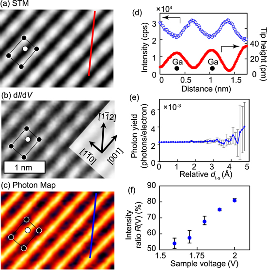
Figure 2. Atomically-resolved STM image, dI/dV map, and STL photon map. (a) An STM image, (b) a dI/dV map, and (c) an STL photon map of GaAs(110) (V = 1.8 V). A unit cell at identical positions is shown (black: Ga, white: As). The STL photon map was measured with an exposure time of 0.2 s/point (64 × 44 points). (d) Line profiles of an STM image and STL photon map (V = 1.8 V, It = 100 pA) along the ![$[11\bar{2}]$](https://content.cld.iop.org/journals/0957-4484/26/36/365402/revision1/nano518085ieqn2.gif) direction, as indicated by the lines in (a) and (c), respectively. (e) Tip–sample distance dependence of the photon yield. Tunnelling current and photon intensity were simultaneously measured while the tip was gradually retracted away from the initial tip–sample distance. The photon yield was calculated from the observed number of photons and the number of injected electrons at each dt-s. Tip–sample distance is measured from the initial distance which is determined by the tunnelling condition of V = 1.8 V, It = 100 pA. (f) Ratio of photon intensity at the Ga site with respect to that at the centre of the unit cell as a function of sample voltage.
direction, as indicated by the lines in (a) and (c), respectively. (e) Tip–sample distance dependence of the photon yield. Tunnelling current and photon intensity were simultaneously measured while the tip was gradually retracted away from the initial tip–sample distance. The photon yield was calculated from the observed number of photons and the number of injected electrons at each dt-s. Tip–sample distance is measured from the initial distance which is determined by the tunnelling condition of V = 1.8 V, It = 100 pA. (f) Ratio of photon intensity at the Ga site with respect to that at the centre of the unit cell as a function of sample voltage.
Download figure:
Standard image High-resolution imageThe correlation between the contrast of an STM image and a photon map can be seen more clearly with line profiles in figure 2(d). A similar observation showing an almost inverted correlation of an STM image with a photon map has been reported on Au(110) , where the luminescence is attributed to radiative decays of interface plasmons localized near the tip–sample gap region. For the case of Au(110), the contrast inversion was explained based on the change in electromagnetic interaction between the STM tip and the metallic sample as a function of the tip–sample distance (dt-s) [11]. To examine the influence of the electromagnetic interaction, we measured the photon yield as a function of dt-s (figure 2(e)), which shows that the photon yield is fairly constant at least for dt-s <2.5 Å (details are described in Supplementary Information). The contrast in the STL photon maps therefore arises from surface non-radiative recombination without any influence of the electromagnetic interaction between the tip and sample.
Local variation in the photon intensity in STL (figure 2(c)) can be analysed by considering local electron-injection into the electronic states distributed on the GaAs(110) surface and dynamic processes of the electrons at the surface. In order to identify the electronic states responsible for the tunnelling, we investigated the electronic structure of GaAs(110) using DFT calculations. Figure 3(a) shows the band structure of the GaAs(110) surface, in which the bulk band structure is also projected for comparison. The first unoccupied surface band (C3 band) has valleys at the Γ- and X-points of the surface Brillouin zone; although the bottoms of these valleys are located at almost identical energy levels, the C3 band is resonant with the bulk CB at Γ-point, and it lies within the energy gap of the projected bulk band at X-point. Because other valleys in the C3 band and the upper unoccupied surface bands are located higher in energy, tunnelling electrons would be dominantly injected into the Γ- and X-valleys of the C3 band, when the sample voltage is slightly above the band gap. Figures 3(b)–(d) show spatial distribution of charge densities ( and
and  of the electronic states in the C3 band at Γ- and Χ-points, i.e.
  and
and  respectively. Figure 3(b) clearly displays that
  penetrates into the bulk whereas
  is localized at the surface. Figure 3(c) shows a relatively uniform distribution of
  on the surface. In contrast,
  is strongly localized around the surface Ga atoms (figure 3(d)), which has a large value at the Ga sites and it becomes very small at the centre of the unit cell. It is expected that when the STM tip is located above the surface Ga atoms
  considerably contributes to the tunnelling, whereas contribution from
  is dominant when the tip is located above the centre of the unit cell.
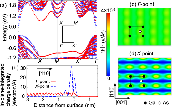
Figure 3. Calculated electronic structure of GaAs(110). (a) Band structure for GaAs(110) surface (red closed circle) and projected bulk band structure (blue open circle). Inset shows the surface Brillouin zone. (b) Charge densities  (I = Γ, Χ) integrated in planes parallel to the surface were plotted as a function of the distance from the surface. (c), (d) Charge densities
  (i = Γ, Χ) in a (110) plane at a distance z = 4 Å above the surface As atom. Similar values of z have been typically used for analyzing the distribution of surface electron density [15, 39]. Charge densities were visualized using VESTA software [40].
Download figure:
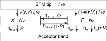
Standard image High-resolution imageAs a next step, we consider dynamics of the electrons injected into the SS using a rate equation approach. A schematic diagram is illustrated in figure 4. We assume that electrons are injected into either  or
or  because the DFT calculation shows that the contributions from other states are negligible in our experimental condition. Rate equations regarding the number of electron NΓ and NΧ in
  and
and  respectively, are given by
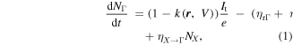

where the ratio of the tunnelling current injected into  to the total tunnelling current It is defined as
  which is a function of STM tip position
  and sample voltage V.
  and
and  are radiative and non-radiative recombination rates in
  (i = Γ, Χ), respectively.
  and
and  are transfer rates of
  and
and  intervalley scattering processes [5, 6], and
  is the element charge. We considered the radiative recombination only at the Γ-point, because the occupied electronic bands at the X-point are far below the VB maximum which is located at the Γ-point (figure 3(a)). This consideration is supported by the fact that no radiative recombination from the electronic states localized at the surface, specifically
  was observed in the STL measurement (figure 1(b)). It is noteworthy that the bottoms of Γ- and Χ-valleys of the C3 band are close in energy and the electrons can be scattered between these valleys [5, 6].
Figure 4. A schematic diagram of the electron energy dissipation.
Download figure:
Standard image High-resolution image
In a steady state, photon intensity induced by the tunnelling current is expressed as

where  is the internal quantum efficiency of the luminescence in the bulk,
  is the probability of
  intervalley scattering, and
  is the probability of non-radiative surface recombination. Concerning the dominant process for the surface non-radiative recombination, Auger [41] and Shockley–Read–Hall [42] processes are considered to be valid because the doping level of our sample is relatively high and unavoidable defects such as vacancies and atomic steps have been observed on the surface.
If we take a ratio of photon intensities  with different
  Y and Q are eliminated from equation (3) and P can be estimated using the experimental results. We define
  which is the ratio of
  with the tip position above the surface Ga atom and above the centre of the unit cell (corresponding experimental data are shown in figure 2(f))

Because  at the Ga site is much larger than that at the centre of the unit cell (figure 3(d)), we can assume
  thus the following relationship is obtained:

The minimum value of R observed in the experiment is 54% at 1.6 V (figure 2(f)). Therefore, we concluded that the non-radiative recombination probability P for electrons in  is at least 46%.
With this result ( Q can be estimated to be greater than 0.995 using the reported value of Y ≈ 0.24 for Zn-doped GaAs with a carrier concentration of 2 × 1019 cm−3 [36] and assuming
  The latter assumption is based on the DFT calculation results which show a negligibly small amount of
  at the unit cell centre (figure 3). The large value for Q, 99.5%, i.e., a high probability of
  intervalley scattering can be explained by the short transfer time
  [5, 6], which is about 1000 times shorter than the recombination lifetime of ∼1 ns in the bulk GaAs [38].
4. Conclusion
In conclusion, we have investigated electron energy dissipation mechanism at the p-type GaAs(110) surface based on atomically-resolved STL observations and theoretical analysis. Tunnelling electrons injected into the surface mainly undergo non-radiative recombination through the SS localized near surface Ga atoms. The probability of non-radiative recombination at the SS was estimated to be more than 46%. In addition, it is suggested that the fast  intervalley scattering prevents the injected electrons from penetrating into the bulk [5, 6], which suppresses luminescence in the bulk. Our results provide novel insights into carrier injection, scattering and recombination processes in electroluminescence of semiconductors. Microscopic analysis of these processes with atomic spatial resolution would contribute to the fundamental understanding of carrier dynamics and energy conversion in nano-materials.
Acknowledgments
This work was financially supported in part by a Grant-in-Aid for Scientific Research (S) (21225001), Scientific Research (A) (15H02025), Research Activity Start-up [26886013] and JSPS Fellows (15J03915) from the Ministry of Education, Culture, Sports, Science and Technology (MEXT) of Japan. Some of the numerical computations presented here were performed using RICC and HOKUSAI systems at RIKEN. We thank David W Chapmon for carefully reading the manuscript and Ryuichi Arafune for helpful discussion.
Supplementary information
Supplemental experiments regarding tip-induced effect were performed.