

Abstract
We report on optically transparent thin film transistors (TFTs) fabricated using multilayered molybdenum disulfide (MoS2) as the active channel, indium tin oxide (ITO) for the back-gated electrode and indium zinc oxide (IZO) for the source/drain electrodes, respectively, which showed more than 81% transmittance in the visible wavelength. In spite of a relatively large Schottky barrier between MoS2 and IZO, the n-type behavior with a field-effect mobility (μeff) of 1.4 cm2 V−1 s−1 was observed in as-fabricated transparent MoS2 TFT. In order to enhance the performances of transparent MoS2 TFTs, a picosecond pulsed laser was selectively irradiated onto the contact region of the IZO electrodes. Following laser annealing, μeff increased to 4.5 cm2 V−1 s−1, and the on-off current ratio (Ion/Ioff) increased to 104, which were attributed to the reduction of the contact resistance between MoS2 and IZO.
Export citation and abstract BibTeX RIS
1. Introduction
The growing desire for a next-generation display has given rise to persistent attempts and efforts to demonstrate optically transparent and mechanically flexible thin-film transistors (TFTs). For a transparent display, a fully transparent thin-film transistor will play an essential role to achieve high transmittance because the TFT backplane in the display has been one of the major factors of reduction in transmittance [1]. In this regard, various new classes of nanomaterials, such as single-walled carbon nanotubes (SWCNTs) or oxide nanowires (NWs), with transparent electrodes have been proposed to achieve ultra-high optical transparency and superior electrical performance due to these one-dimensional semiconductors of molecular thickness [2–8]. Despite the significant progress, a critical weakness remains and must be further improved in their commercial integrated circuit. The challenges to reach a commercial display requires a novel nano-semiconductor to achieve optical transparency, high-mobility and amenability to a large-area growth technique.
Recently, a series of transition metal dichacogenides (TMDCs), especially two-dimensional (2D) molybdenum disulfide (MoS2), can be an attractive candidate for transparent electronics due to their relatively high mobility (>80 cm2 V−1 s−1), finite bandgap (1−2 eV) and ultra-thin 2D layered structure [9–14]. 2D layered MoS2 transistors have been well studied as the architecture of the Schottky device in which source/drain metals were directly deposited on active channels of TMDC. To date, the n-type behavior of the MoS2 transistor results in the fact that the Fermi level of the source/drain metal is pinned in the vicinity of the conduction band of MoS2; thus, a relatively low work-function metal, such as titanium (Ti) or Scandium (Sc), brings about the small Schottky barrier (SB) height to the conduction band [13–17]. However, the conventional transparent metals, indium tin oxide (ITO) or indium zinc oxide (IZO), have the high work function with a work function of ∼5.1 eV [18, 19]. The large SB height with the IZO-contacted MoS2 transistor has limits in its use in the high-performance of transparent devices [20].
Here, we explore transparent multilayer MoS2 TFTs with ITO for the back-gated electrode and IZO for the source/drain electrodes, respectively. In order to realize the high performance of the transparent MoS2 transistor, selective laser annealing enables the achievement of superb interfacial characteristics between the IZO electrode and MoS2 material contact surface and is also useful for a reduction in contact resistance. The irradiation of a pulsed laser with high energy density and a short wavelength onto transparent electrodes leads to the thermal annealing effect at the locally confined small area that needs high temperature without extreme thermal damage. The electrical properties of the laser-annealed transparent MoS2 TFTs were clearly enhanced, and the average transmittance in the overall devices was estimated at ∼81% in the visible wavelength range.
2. Experimental
Figure 1(a) presents a three-dimensional (3D) schematic illustration of the transparent multilayer-MoS2 TFT with a back-gated structure in a cross-sectional view. The ITO glass with a ITO thickness of 200 nm and a sheet resistance of 10–15 Ω sq−1, respectively, was used as the back-gated electrode of the TFTs. A 300 nm thick SiO2 as the gate dielectric was deposited on the ITO glass by plasma-enhanced chemical vapor deposition (Low Stress PECVD, SLP-730 by Unaxis) at 350 °C. Mechanically exfoliated multilayer MoS2 from bulk MoS2 (SPI supplies, USA) is transferred on the SiO2 layer [13, 14]. Then, the IZO layer with a thickness of 100 nm as the source/drain electrodes was deposited by sputtering. The IZO source/drain electrodes with various channel lengths were fabricated using conventional photolithography and the etching method. Figure 1(b) shows the transmission spectra (Agilent 8453 UV–vis Spectrophotometer) of transparent MoS2 TFTs on the glass substrate and on the ITO glass in the 300–900 nm wavelength range. The 1 × 1 cm2 area contains 2240 transistor patterns, and about 92% of the area is covered with IZO electrodes. It should be noted that multilayer MoS2 flakes were randomly distributed in our device configuration. However, the active layer of each TFT in the driving circuitry (for example, six transistors and two capacitors) occupies very limited space in the whole display panel. Also, the overall transmittance of the patterned active layer (e.g. discontinuous layer structure) would be correlated with the summation of each active area. In addition, the reduction of transmittance due to the signal line between the TFT circuit and light-emitting component also plays the important role of estimating the optical transparency of the display panel. So, we believe that our device configuration could evaluate the potential optical transparency of transparent TFT arrays, which have a similar area of the total active layer. The averaged transmittances of our transparent MoS2 TFTs and ITO glass were ∼81% and ∼87%, respectively, in the visible wavelength range. The transmittance of MoS2 TFTs was almost comparable to that of ITO glass in the wavelength range of 450–650 nm, which was most sensitive to response of the human eye. An optical microscope image (Olympus BX51M) of the transparent MoS2 TFTs on printed texts are presented in figure 1(c). We can clearly identify the texts through the MoS2 TFTs as well as through the colored IZO electrodes. The inset of figure 1(c) shows a single TFT that consists of a multilayered MoS2 flake between the IZO source/drain electrodes.
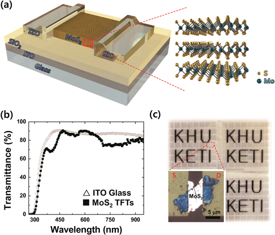
Figure 1. (a) 3D cross-sectional schematic view of the transparent multilayered MoS2 TFT. The dashed red line indicates atomic arrangements and a layered structure in multilayer MoS2. (b) Transmission spectra of the ITO glass (△) and the transparent MoS2 TFTs (■) in the visible wavelength range. (c) Optical microscope image of the transparent MoS2 TFTs on the printed texts. Inset: magnified optical microscope image of a single TFT consisting of a MoS2 flake between the IZO source and drain electrodes.
Download figure:
Standard image High-resolution imageFigure 2(a) represents the schematic illustration of the selective laser annealing process at the contact regions between MoS2 and the source/drain electrodes using an yttrium vanadate (Nd:YVO4) picosecond pulsed laser (Newport Corp., USA) operating at a wavelength of 355 nm, a pulse repetition rate of 80 MHz, a pulse width based on the full width at half maximum of 12 ps and a power of 26.8 mW, respectively. The short wavelength (355 nm) helps the transparent electrode efficiently absorb more energy from the incident light of the laser. The 100 nm thickness of IZO showed 30–36% transmittance at 355 nm [21]. 64–70% of the laser energy would be absorbed in the IZO electrodes, and the rest of the energy might reach, and be absorbed in, the MoS2 layer. In addition, the high repetition rate (80 MHz) causes heat accumulation effects because the temperature cannot cool down to below the working ambient temperature before the next pulse arrives [22]. The accumulated heat is enough to induce changes of the interfacial characteristics of IZO-MoS2 and might have led to a possible laser annealing process. The Gaussian-type laser beam with a diameter of 1.5 μm was mainly irradiated along the edge of the contact of the target sample placed on a high-resolution x-y positioning stage (Aerotech Inc., USA). The laser power, scan speed of the stage, optical shutter and beam path were simultaneously operated by a computer during the annealing process. The details of the experimental conditions were reported earlier [23].

Figure 2. (a) Schematic illustration of the selective laser annealing process. (b) Comparison of the Ids−Vds characteristic curves of transparent MoS2 TFT at Vg = 0 V before (■) and after (□) laser annealing. Inset: Ids−Vds characteristic curves of transparent MoS2 TFT (Vg = 0 V) using the logarithmic scale.
Download figure:
Standard image High-resolution image3. Results and discussion
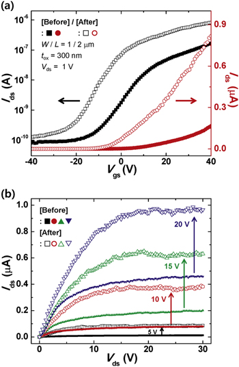
The source-drain current and voltage (Ids−Vds) characteristic curves of the transparent MoS2 TFT as two-terminal devices (gate was grounded, i.e. at Vgs = 0 V) before and after laser annealing are compared in figure 2(b). The Ids−Vds characteristic curves of the pristine (before laser annealing) transparent MoS2 TFT showed typical n-type diode-like behavior, and the current level of the device was dramatically increased after laser annealing treatment. In order to investigate the change of the charge transport due to the laser annealing, the Ids−Vds characteristic curves of the transparent MoS2 TFT (Vg = 0 V) were re-plotted using the logarithmic scale, as shown in the inset of figure 2(b). For pristine transparent MoS2 TFT, two distinct regimes, depending on the slopes of the Ids at Vg = 0 V, were observed. In a low-biased region, the Ids increased linearly (I ∝ V), indicating the ohmic conduction due to the thermionic emission. However, the Ids increased quadratically (I ∝ V2) in the high-biased region, which could be explained through the space charge limited current model [24, 25]. Kwon et al reported on the decrease of the Schottky barrier width in the picosecond laser-annealed MoS2 TFT with titanium-gold electrodes, which resulted in the reduction of the contact resistance between MoS2 and the metal electrodes [23]. The enhancement of the current level and the change of the slopes in the log-log plot of the Ids−Vds characteristic curves suggested that charge carriers would be more effectively injected from the IZO electrode to the MoS2 active layer due to the laser annealing process, which well agreed with the previous reports [23–25].
Figures 3(a) and (b) show the comparison of the transfer and output characteristic curves of the transparent MoS2 TFT with respect to the laser annealing process. It is noted that the electrical characteristics were measured in the same MoS2 TFT for investigating the effects of the laser annealing treatment. As shown in figure 3(a), the field effect mobility (μeff = Lgm/WCoxVds) of the as-fabricated MoS2 TFT was calculated as 1.4 cm2 V−1 s−1 in the linear region (Vds = 1 V). It has been known that there exists a large Schottky barrier (∼0.7 eV) between IZO and MoS2 due to the high work function of IZO (∼5 eV), which can severely restrict electron transport at source/drain contacts. Recently, Hinkle et al reported that the electronic properties of multilayered MoS2 could be significantly varied with the spatial point even within the same sample [16]. Depending on the stoichiometric variation of sulfur to the molybdenum ratio, the intrinsic defects of the natural MoS2 could be categorized into S-rich (S:Mo = 2.3:1) and S-deficient (1.8:1) species, which would result in p-type and n-type characteristics, respectively [16, 26]. The S-deficient defects were estimated to metallic-like properties with a relatively low effective work function, which lead to the inhomogeneous interface between IZO and MoS2. Although a relative low density of 0.1–5%, lowering of the Schottky barrier height due to the S-deficient defects could be attributed by considering a parallel conduction model [16]. The n-type behaviors of the electrical properties, observed in figures 2 and 3, indicated that S-deficient defects would be dominant in the MoS2 active layer in our transparent TFT. Das et al reported that the Fermi levels of metals with high work functions, such as nickel (5.0 eV) and platinum (5.9 eV), were also pinned in the conduction band edge of the MoS2 [15]. So, the n-type behavior of the transparent MoS2 TFTs could also be attributed to the Fermi level pinning between the MoS2 and IZO [15].
Figure 3. (a) Transfer characteristic curves (Vgs−Ids) of the transparent MoS2 TFT at Vds = 1 V before (solid) and after (open symbols) laser annealing. The channel length (L) and width (W) were equal to 2 and 1 μm, respectively. (b) Output characteristic (Vds−Ids) curves of the transparent MoS2 TFT with different gate biases (Vgs = 5, 10, 15 and 20 V) before (solid) and after (open symbols) laser annealing.
Download figure:
Standard image High-resolution image
The laser annealing treatment allowed about fivefold enhancement of the on-current (Ion), while the off-current (Ioff) levels of the device were hardly changed. The on/off current ratio (Ion/Ioff) of the laser annealed device approached ∼104. After the laser annealing treatment, the field effect mobility of the device was threefold increased (4.5 cm2 V−1 s−1). Based on the output characteristic curves of the MoS2 TFT shown in figure 3(b), the improvement of the contact behavior in the low Vds region and the robust current saturation at the high Vds region were observed after laser annealing. The enhancement of the TFT performances due to the laser annealing treatment was in good agreement with the results shown in figure 2. It is known that the composition of the IZO film is changed over 300 °C [27], which can be induced at the IZO-MoS2 interface by laser annealing. There seems to be oxygen poor environments at the bottom of the IZO electrode at the IZO-MoS2 interface in which an oxygen deficient defect can be produced by heat generated through laser annealing. The conductivity of the interfacial side in IZO electrodes would increase due to these oxygen deficient defects, resulting in the reduction of contact resistance between IZO and MoS2 [28, 29].
4. Conclusion
In conclusion, we successfully fabricated transparent multilayered MoS2 TFTs using conventional transparent conducting oxide electrodes such as ITO and IZO. Our transparent TFTs showed more than 81% transmittance in the visible wavelength range. Even taking into account the high work function of IZO, the transparent MoS2 TFTs exhibited quite moderate electrical performances because of the intrinsic defects in natural MoS2, which would play a role in lowering the Schottky barrier height. In order to boost the electrical performances of those samples, the picosecond laser annealing treatment was selectively applied onto the contact regions between the MoS2 and IZO source/drain electrodes. As a result, the field-effect mobility and the on/off current ratio of the transparent MoS2 TFTs approached up to 4.5 cm2 V−1 s−1 and ∼104, respectively. Although future works will include controlling the defects' concentration and optimizing the electrical properties as well as the transmittance, these results indicate potential possibilities for applications in future transparent display devices using multilayer MoS2 TFTs with conventional IZO contacts.
Acknowledgement
This research was supported by the Industrial Strategic Technology Development Program (10045145) and the Basic Science Research Program (2012R1A1A1042630).