

Abstract
A systematic method to control the porosity of silicon nanowires is presented. This method is based on metal-assisted chemical etching (MACE) and takes advantage of an HF/H2O2 etching solution and a silver catalyst in the form of a thin patterned film deposited on a doped silicon wafer. It is found that the porosity of the etched nanowires can be controlled by the doping level of the wafer. For low doping concentrations, the wires are primarily crystalline and surrounded by only a very thin layer of porous silicon (pSi) layer, while for highly doped silicon, they are porous in their entire volume. We performed a series of controlled experiments to conclude that there exists a well-defined critical doping concentration separating the crystalline and porous regimes. Furthermore, transmission electron microscopy investigations showed that the pSi has also a crystalline morphology on a length scale smaller than the pore size, determined from positron annihilation lifetime spectroscopy to be mesoscopic. Based on the experimental evidence, we devise a theoretical model of the pSi formation during MACE and apply it for better control of the nanowire morphology.
Export citation and abstract BibTeX RIS
1. Introduction
Nanostructured silicon, in particular silicon nanowires (SiNWs), porous silicon (pSi) or silicon nanocrystals, has attracted great attention in recent years due to its potential applications in photonics [1], optoelectronics, electronics [2, 3] and fabrication of thermoelectric devices [4, 5]. One of the promising methods of obtaining NWs with exactly tailored properties is metal-assisted chemical etching (MACE) [6–8]. The method allows precise tuning of the length, density, ordering and diameter of the NWs. For example the diameter can be varied between several μm and down to 10 nm [9], where quantum phenomena dominate.
While the MACE preparation of NWs is well established [7], the understanding of the underlying physical and chemical processes is not complete. For example, the morphology of the NWs can be varied in full range between mono-crystalline and mesoporous. While the effect itself has been already observed [10], no comprehensive model of its microscopic mechanism exists. In this paper, we present results of a series of controlled experiments and form a hypothesis explaining the variation of the morphology.
Subsequently, we use the results to fabricate NWs with precisely prescribed morphology.
The paper is organized as follows. First, we describe briefly the MACE procedure and characterize obtained NWs. Second, based on these results, we build an analogy between MACE and well-studied case of anodic etching [11–14], which leads to our model. Finally, we use the model to fabricate NWs of particular morphology.
2. Experimental
2.1. Fabrication of SiNWs by MACE
SiNWs were fabricated by means of the well-established MACE method as described by Huang et al [7]. The approach involves two steps. First, a lithographically structured noble metal film (Ag, Au, Pt, Pd) is deposited on the Si substrate. Subsequently, the etching is performed in HF and an oxidative agent, typically H2O2.
Different commercial Si substrates with doping levels ranging from 1012 to 1019 cm−3 (p- as well as n-doped) have been used as starting material. The Si surface was cleaned by an RCA-I treatment [15] and rinsed with deionized water. For lithographic structuring, nanosphere lithography was used [16]. Here, monodispersed polystyrene (PS) particles (commercially available from the Microparticles GmbH Company as a 10 wt% solution) were deposited on the cleaned surface by means of a Langmuir–Blodgett technique, resulting in a hexagonally closed-packed monolayer of the particles. Afterwards, oxygen plasma at a low process pressure of 0.06 mbar and an oxygen flow of 160 sccm min−1 (Diener Electronic plasma cleaner 'Nano') was applied in order to reduce the diameter of the spheres. The diameter of the spheres could be controlled by varying the plasma etching time. Subsequently, a 60 nm thick silver film was deposited by thermal evaporation (model B 30.2, HVT Dresden) onto the masked substrate. After removing the PS spheres in an ultrasonic bath consisting of CH2Cl2, a silver mask with highly ordered openings remains. Finally, the silver masked substrates were etched for 10 min in a solution consisting of 5.65 mol L−1 HF and 0.1 mol L−1 H2O2 leading to the formation of SiNWs. The whole procedure was carried out at room temperature in darkness. The silver was removed by nitric acid.
2.2. Tailoring the morphology of SiNWs
We performed numerous experiments in the whole parameter space spanned by the H2O2 concentration, the HF concentration, the process temperature and the doping type, dopant and doping level of the Si wafers. In general, following the Nernst equation, both an elevated temperature and a high H2O2 concentration enhance the redox potential of the etching solution and thus, the etching rate. As a rule, pSi is formed for every doping type and level when these two parameters are high enough. However, for the sake of the stability of the process, it is important to keep the parameters in a moderate regime. The following results pertain to fixed values of the temperature (room temperature) and H2O2 concentration (0.1 mol L−1). The concentration of HF was fixed to 5.65 mol L−1, but the latter parameter hardly influences the morphology.
It turned out that for the values given above the morphology is determined by the doping concentration alone. In particular, it does not depend on the dopant type. Therefore, in what follows we concentrate more closely on relation between doping level and morphology.
We began with commercially available n- and p-doped Si substrates with doping levels between 1012 and 1019 cm−3, listed in table 1. We followed the procedure described in section 2.1 with the parameters of the etching solution specified above. The scanning electron microscope (SEM, using a Philips XL30 FEG ESEM) characterization of resulting structures shows clearly that NWs etched from highly doped Si were always completely porous (figures 1(a) and (b)), while NWs from slightly doped material were primarily single-crystalline (figures 1(c) and (d)), surrounded only by a relatively thin pSi layer [17].

Figure 1. SEM images of etched wires from (a) a highly doped Si substrate (Si(100), B-doped,1 × 1019–2 × 1019 cm−3) and (c) a slightly doped Si substrate (Si(100), B-doped,  (b) and (d) show a higher magnification of the areas marked in (a) and (c), respectively. In the case of highly doped wires, a porous structure formed beneath the wire, while the slightly doped material appears to be single crystalline.
Download figure:
Standard image High-resolution imageThe commercially available doped substrates do not allow a gradual variation of the doping concentration and type. Thus, it is not possible to establish whether the transition between crystalline and porous NW morphology is abrupt and at which doping level it occurs. Therefore, we devised an experiment in which we gradually vary the doping level of the NWs, keeping the dopant type unchanged. The remaining process parameters are kept constant as well. Multiple boron-doped Si layers of gradually varying doping level in the range of 6 × 10¹⁷–6 × 1018 cm−3 were grown epitaxially by means of molecular beam epitaxy (MBE, using a Riber SIVA 45 instrument) at 500 °C and a deposition rate of 0.5 Å s−1. The layers were grown on an P-doped Si(100) substrate with a doping level of 1 × 10¹⁵–2 × 1015 cm−3. Prior to the MBE growth, organic contaminants on the surface of the substrate were removed by an RCA-I cleaning [15]. The layers had a thickness of 30 nm each. An additional layer of 140 nm thickness and a high doping level (1018 cm−3) was deposited on the top of the layer stack. It covered the stack to provide protection against etching away the top of the NW during MACE. The boron concentration was measured afterwards by secondary ion mass spectroscopy. The Si layers were separated by additional 0.4 nm thick Ge layers deposited by MBE with a growth of 0.2 Å s−1. The additional Ge layers played the role of markers allowing an easier differentiation between the layers of different doping levels in transmission electron microscopy (TEM, using a JEOL JEM 4010) characterization. The samples with the fabricated boron-doped layers and spacers were used as starting material for the fabrication of NWs exactly as outlined in section 2.1.
Figure 2(a) shows the TEM image of an etched NW. Layers of different boron concentrations separated by thinner spacers are discernible; they are labeled in the figure. The slightly doped Si layers exhibit a crystalline structure (figure 2(b)), while the highly doped Si layers are clearly porous (figure 2(c)). We observe that the transition between crystalline and porous Si is rather abrupt and takes place around the critical doping level between 1 × 10¹⁸ and 3 × 1018 cm−3. It should be noted that the value pertains to our process parameters defined in section 2.1.
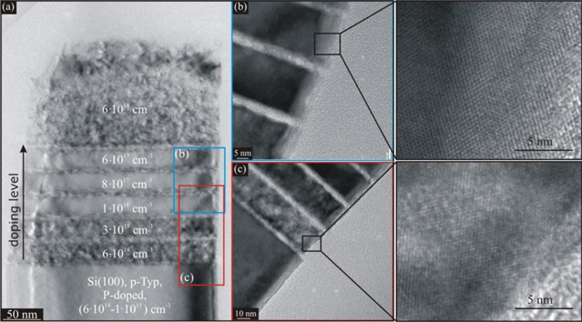
Figure 2. (a) TEM image of an etched Si wire with Si layers doped in the range of 6 × 10¹⁷–6 × 1018 cm−3. (b) Slightly doped Si layers are crystalline, and (c) highly doped Si layers are porous. The transition from single-crystalline to a porous morphology is found in the range of 1 × 10¹⁸–3 × 1018 cm−3.
Download figure:
Standard image High-resolution imageWe also observe that the Ge is etched away more intensively than Si. It is a consequence of the fact that GeO dissolves rapidly in H2O; a detailed study of this phenomenon is presented in [18].
2.3. Systematic characterization of etched pSi material
In what follows, we present the more detailed characterization of the pSi NWs obtained by means of high resolution transmission electron microscope (HRTEM, using a JEOL JEM 4010), energy dispersive x-ray spectroscopy (EDX) and electron energy loss spectroscopy (EELS) using a Philips CM 20 FEG transmission electron microscope with an acceleration voltage of 200 kV. We concentrate on the wires with high doping levels (1019 cm−3). We aim to explain why only highly doped Si results in porous NWs. The pSi obtained by MACE described above resembles closely the pSi originating from well-studied anodic etching, and we assume that similar processes take place in both cases.
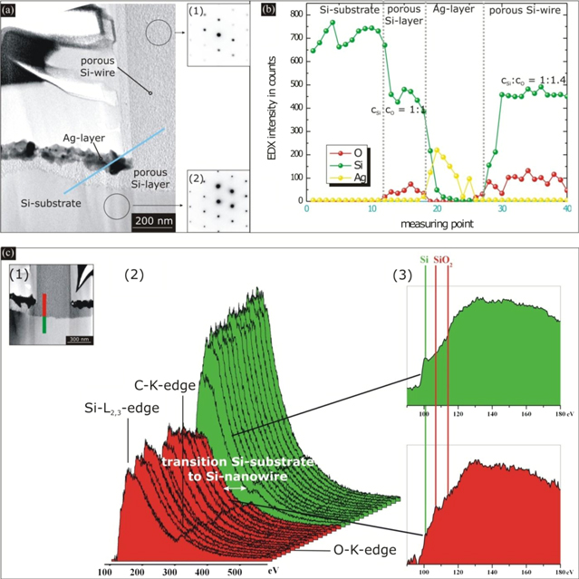
To examine the effect of porosity on the crystal quality of the NWs, electron diffraction patterns from bulk Si and from pSi NWs were taken, cf figure 3(a). The diffraction patterns show that the crystalline order of the silicon was not perturbed during the formation of the porous structure, cf the insets (1) and (2) in figure 3(a). We note that the same was observed after anodic etching [14].
Figure 3. (a) TEM image of an etched Si wire from highly doped Si material (as-doped, 1 × 10¹⁹–2 × 1019 cm−3). Electron diffraction patterns of the porous wire show that the crystallinity was preserved during the etching process. Along the marked blue line, EDX measurements were carried out. (b) EDX intensities of the Si-Kα, O-Kα and Ag-Lα line. (c) EELS investigations: (1) TEM image of a cross section of a wire. Measurements were carried out along the marked red–green line. (2) EELS spectra after subtracting the background. (3) Fine structure of the Si-L2,3 edge of the marked spectra.
Download figure:
Standard image High-resolution image
Furthermore, the NWs were analyzed quantitatively using EDX (along the blue line in figure 3(a)) in four characteristic areas: the crystalline Si substrate, the porous Si layer beneath the silver film, the silver layer, and the porous Si NWs. The EDX intensities of the Si-Kα, O-Kα and Ag-Kα lines are shown in figure 3(b). The measurements show that the porous structure consists of both Si and O. The ratio of Si to O in the area of the pSiNWs amounts to about 1:1.4. The type of the Si–O binding cannot be unambiguously determined by means of EDX, and we resort to EELS for a closer study.
The spectra were taken along the red–green line in figure 3((c), panel 1). The red part of the line comprises the measurements in the area of the pSiNW, while the green line is part of the crystalline Si substrate. Next to this, the resulting EELS spectra are shown after subtracting the background, figure 3((c), panel 2). Three typical edges can be identified: the silicon edge, the carbon edge (caused by the embedding glue of the cross-section sample prepared by a focused ion beam) and the oxygen edge.
The fine structure of the energy loss spectra (electron energy loss near fine edge structure, ELNES) yields information about the binding state of Si. The fine structure of the Si-L2,3 edge allows us to analyze the binding of an Si atom with its nearest atomic neighbors. In particular, we can differentiate between Si–Si bindings and Si–O bindings.
Figure 3((c), panel 3) shows the fine structure of the Si-L2,3-edge of two spectra near the border between the substrate and the NW. The green spectrum exhibits a clear Si peak at the energy loss of 100.5 eV, typical for Si–Si bonds [19]. In the area of the NW, the appearance of the spectra abruptly changes. Only a weak shoulder can be seen at 100.5 eV, while a double peak emerges at an energy of about 108 and 114.5 eV. This double peak is typical for Si with an oxygen environment [19]. Altogether, the fine structure points at an overlap of spectra corresponding to Si–Si and Si–O bonds.
The pore size of the pSi was further investigated by means of positron annihilation lifetime spectroscopy. Pulsed monoenergetic positrons were generated by pair production using the 40 MeV electron beam at the ELBE radiation source (Helmholtz Zentrum Dresden Rossendorf) [20]. In mesoporous material, ortho-positronium with a characteristic lifetime can be detected [21]. In pSi, the lifetime amounted to τ = (80.8 ± 19.5) ns with an intensity of 1.66%. With the positron lifetimes measured the pore size is calculated to (6.9 ± 2.8) nm. In agreement with the classification of anodically etched porous materials [11], the Si can be regarded as mesoporous.
With the experimental results at hand, we are now able to give a theoretical model.
3. Formation of pSi—a theory
Our experiments have shown that the porosity of NWs obtained in MACE is a function of the doping concentration of the Si substrate. Here, we can draw an analogy to anodic etching. The anodically etched pSi formed by the application of a bias with a HF-based solution is also determined by the doping concentration [12, 14]. This becomes evident by considering the relationship between the doping concentration ND/A and the width of the space-charge region (SCR) for metal-semiconductor contacts [15].

Herein,  is the permittivity of the vacuum,
  the permittivity of the material (Si:
  UB the barrier height, U the applied bias in forward direction and
  the doping concentration. The SCR presents a region depleted of majority charge carriers, where the entire potential drop occurs. The larger the doping concentration
  the narrower the potential barrier. In the case of a narrow SCR, the charge carriers may tunnel. This occurs for doping concentrations above 1018 cm−3, where the rectifying property of the contact vanishes. On the other hand, in the case of small concentrations, the transport involving the thermal excitation of carriers above the barrier, called thermionic emission, dominates.
The theory can be applied to MACE as well. Here, we encounter the electrolyte–Si interface as well and similarly to the anodic etching described above the charge transport occurs more efficiently in the case of highly doped Si, which results in the rapid formation of the pSi. However, in contrast to anodically etched pSi, where the charge transfer is controlled by the applied voltage, the charge transfer in MACE is of different nature. The description of the mechanism involved has been recently described in detail in [17], and here we repeat it briefly for completeness. The charges necessary for the formation of the pSi originate from the catalytic reaction of the oxidative agent H2O2 at the surface of the silver. Ag+ ions are formed from elemental Ag by the reduction of H2O2


Subsequently, the charge transport is facilitated primarily by Ag/Ag+ redox pairs circulating in the electrolyte in the porous layer beneath the silver film forming during the etching [17, 22]. The process provides electronic holes required for the oxidation of Si and its subsequent solution by HF. At the Si–electrolyte interface, Si is solved by HF according to the following reaction equation

As discussed above, the SCR is narrow in the case of highly doped Si and allows the efficient transport of electronic holes in both directions, i.e. to and from the Si bulk, by means of tunneling. In this case, the charge transport based on the Ag/Ag+ redox pairs is enhanced by the charge transfer in the low-resistance crystalline substrate. This additional charge transport channel accelerates the divalent etching of Si and thus the formation of the pSi. In the opposite case of slightly doped material the additional charge transport channel is closed and the growth of pSi proceeds much more slowly since it is supported only by the Ag/Ag+ redox pairs circulation and the resulting SiNWs are predominantly crystalline with a thin pSi layer around.
4. Summary and outlook
The morphology of SiNWs by MACE depends strongly on the doping concentration of the starting material. In analogy to anodic etching, porous material is obtained from highly doped silicon, while slightly doped silicon generates crystalline SiNWs. Knowing the critical doping level, we can regulate the morphology of the nanostructures.
Crystalline NWs are widely used for photonic and optoelectronic applications. In some cases, it is advantageous to use crystalline SiNWs with a high doping concentration, a case especially interesting for electric measurements. In accordance with our investigations it is impossible to prepare such structures by standard MACE from highly doped silicon. One way to circumvent the limitation is ex situ doping after etching of slightly-doped starting material. Suitable methods tested by us are the ion implantation [23] or the spin-on dopant technique [24].
Porous highly doped NWs are important in the applications in the bio- and chemical sensors. Another rapidly emerging application field is the NW-based photovoltaics because of the high area-to-volume ratio of these structures. The porosity of NW may be important for thermoelectric applications. The porosity enhances the phonon scattering and thus reduces the thermal conductivity leading to a higher figure of merit ZT [25].
In conclusion, we can tailor precisely the morphology of SiNWs by controlled use of doped Si as starting material.
Table 1. Characteristics of the silicon wafers used for the investigationof the influence of temperature, H2O2-concentration and doping level on the morphology of the silicon nanowires.
| Substrate number and crystal order | Doping element | Specific resistance (Ω cm) | Doping concentration in (cm−3) |
|---|---|---|---|
| I (111) | P (n) | 1000–4000 | 3 × 10¹²–4 × 10¹² |
| II (100) | P (n) | 59.5–80.5 | 5 × 10¹³–7 × 10¹⁴ |
| III (111) | P (n) | 10–20 | 2 × 10¹⁴–4 × 10¹⁴ |
| IV (100) | P (n) | 4–7 | 6 × 10¹⁴–1 × 10¹⁵ |
| V (100) | B (p) | 5–10 | 1 × 10¹⁵–3 × 10¹⁵ |
| VI (100) | B (p) | 6–10 | 1 × 10¹⁵–2 × 10¹⁵ |
| VII (111) | P (n) | 10–20 | 2 × 10¹⁴–4 × 10¹⁴ |
| VIII (111) | B (p) | 0.012–0.016 | 4 × 10¹⁸–6 × 10¹⁸ |
| IX (100) | B (p) | 0.01–0.05 | 8 × 10¹⁸–2 × 10¹⁹ |
| X (100) | B (p) | 0.004–0.007 | 1 × 10¹⁹–2 × 10¹⁹ |
| XI (111) | As (n) | 0.005–0.007 | 1 × 10¹⁸–1 × 10¹⁹ |
Acknowledgments
Technical support by S Schlenker (IZM Halle), W Erfurth (MPI Halle), H Blumtritt (MPI Halle), S Hopfe (MPI Halle) and C Münx (MPI Halle) as well as the funding by the BMBF project 'SiGe-TE' are gratefully acknowledged. The authors also thank Dr Pawel Adam Buczek for inspiring discussions (EHW).