

Abstract
The hydrogen gas-sensing properties have been investigated of two types of thermochemical hydrogen (TCH) sensors composed of thermoelectric layers based on chalcogenide nanowire arrays and anodic aluminum oxide (AAO) templates. The monomorphic-type TCH sensor, which had only Bi2Te3 nanowire arrays, showed an output signal of 23.7 μV in response to 5 vol% hydrogen gas at room temperature, whereas an output signal of 215 μV was obtained from an n–p junction-type TCH sensor made of connected Bi2Te3 and Sb2Te3 nanowire arrays in an AAO template. Despite its small deposition area, the output signal of the n–p sensor was more than nine times that of the monomorphic sensor. This observation can be explained by the difference in electrical connections (parallel and serial conversions) in the TCH sensor between each type of nanowire array. Also, our n–p sensor had a wide detection range for hydrogen gas (from 400 ppm to 45 vol%) and a fast response time of 1.3 s at room temperature without requiring external power.
Export citation and abstract BibTeX RIS
1. Introduction
Hydrogen gas sensors have attracted much attention recently due to increased interest in hydrogen gas for renewable energy applications; hydrogen is environmentally friendly and does not produce carbon emissions. [1] However, because hydrogen gas is odorless and colorless and has a wide range of explosive concentrations, hydrogen gas sensors are needed to detect its presence. There are many necessary conditions for hydrogen gas sensors to enable their application in various fields, such as high sensitivity, long lifetime, fast response time, moisture resistance and wide detection range. Many types of hydrogen sensors have been reported, including semiconductor-type sensors [2, 3], catalytic combustion-type sensors [4, 5], and electrochemical-based sensors [6, 7]; of these, semiconductor-type and catalytic combustion-type sensors have been commercially developed. However, these sensors have important weaknesses. For example, semiconductor-type sensors, which are mainly constructed using tin dioxide (SnO2) [8], must be operated at high temperature to be effective, increasing power consumption. For catalytic combustion-type sensors, detection of low concentration of hydrogen is not possible because the resistivity change is small at low concentration compared with the semiconductor-type sensor [9]. Palladium (Pd)-based sensors have often been used, but are susceptible to performance degradation when operated continuously in high concentrations of hydrogen gas. Research activities are underway to improve these shortcomings through a variety of approaches.
One alternative, thermoelectric (TE) sensors, were first suggested by McAleer et al [10] and have many advantages such as high stability, low power consumption and reliability. They are based on TE behaviors such as the Seebeck effect, whereby an electric signal is generated as a result of the exothermic oxidation of hydrogen gas at room temperature, without requiring external power. Detailed mechanism is as follows; when molecular H2 and O2 act on platinum catalyst, energy is released as a heat source and molecular of H2 and O2 is combine to form the water (H2O) simultaneously. Here, catalytic formation of water from H2/O2 reaction is consequence of the exothermicity, which play major a role in TE based hydrogen sensor. Various studies have been performed to improve the performance of TE sensors for practical applications. Shin et al [11] fabricated a micro-TE hydrogen sensor based on a thick ceramic film; this sensor had a detection range of 25 ppm to 3%. Nishibori et al [12] developed micro-TE hydrogen sensors with the wide detection range of 10–40 000 ppm, and tested them with various hydrogen concentrations for one year. However, these hydrogen sensors have complicated structures that make them difficult to be produced cost-effectively. Actually, there are few present studies addressing wide range detection up to 4% or response times under high hydrogen gas concentrations; these issues should also be addressed to enable practical applications such as fuel cells for vehicular transportation.
One-dimensional nanostructures have attracted much attention in TEs because thermal conductivity in low-dimensional systems can be reduced by increased interfacial phonon scattering, resulting in rapid charge transport and improved TE performance [13]. There are many methods to synthesize one-dimensional nanostructures, including chemical vapor deposition [14], physical vapor deposition [15], and electrochemical deposition [16]. In the context of TEs, electrochemical deposition has many advantages such as high growth rate, relatively low-temperature growth conditions, and facile control of the shape and size of the nanowires [17]. Above all, this method can be employed to inexpensively fabricate various devices by directly using a porous template such as an anodic aluminum oxide (AAO) template, and can be carried out at room temperature without requiring any high vacuum processes, unlike processing based on silicon wafers. In this research, we suggest for the first time a new type of thermochemical hydrogen (TCH) sensor based on a combination of TE nanowire arrays composed of n-type and p-type chalcogenide materials synthesized by electrochemical deposition on an AAO template, coated with an exothermic catalyst. The hydrogen sensing properties of the TCH sensor were systemically investigated; these included output voltage signal, lower detection limit (LDL) and response time at room temperature.
2. Experimental
2.1. Fabrication of the TCH sensor
The electrolyte used to synthesize the BixTe1−x nanowires was prepared by dissolving TeO2 (99.995%, Alfa Aesar, Inc.) and Bi(NO3)3·5H2O (98%, Acros Organic) in concentrated nitric acid (60%, Junsei Chemical). The electrolyte used to synthesize the SbxTe1−x nanowires was prepared by separately dissolving TeO2 in nitric acid and dissolving Sb2O3 (99.9%, Sigma Aldrich) in L-tartaric acid (99.5%, Sigma Aldrich) solution, and then mixing the two solutions to make an electrolyte consisting of 0.02 M SbO+, 0.01 M HTeO2+, 0.5 M L-tartaric acid and 1 M nitric acid. All electrochemical depositions were carried out in a 250 ml electrochemical cell using a potentiostat (AMETEK, VersaSTAT3) with a standard three-electrode cell, which consisted of Ag/AgCl as the reference electrode, a platinum-coated titanium strip as the counter electrode and aluminum as the working electrode. In all sensors, a 200 nm thick gold seed layer was first deposited onto an AAO template by means of sputtering to enable subsequent plating of nanowires inside the template.
Herein, we fabricated two types of TCH sensors. One was a monomorphic-type TCH sensor composed of an n-type Bi2Te3 nanowire array; the process used to produce this sample is illustrated in figures 1(a)–(d). A gold layer was deposited onto an AAO template with a 200 nm pore size; this layer served both as a working electrode and as a seed layer for the Bi2Te3 nanowires (figure 1(b)). Electrochemical deposition of the Bi2Te3 nanowires into the template was carried out by applying a voltage (figure 1(c)), and then gold nanowire array were deposited using electrodeposition with gold electrolyte (Techni Gold 25 RTU, TECHNIC) over the Bi2Te3 nanowire arrays to form low-resistance Ohmic contacts at the interface between the Bi2Te3 nanowires and the electrode, which was deposited by means of sputtering (figure 1(d)). It is important to assure Ohmic contact because high resistance in a TE device can decrease its TE efficiency.
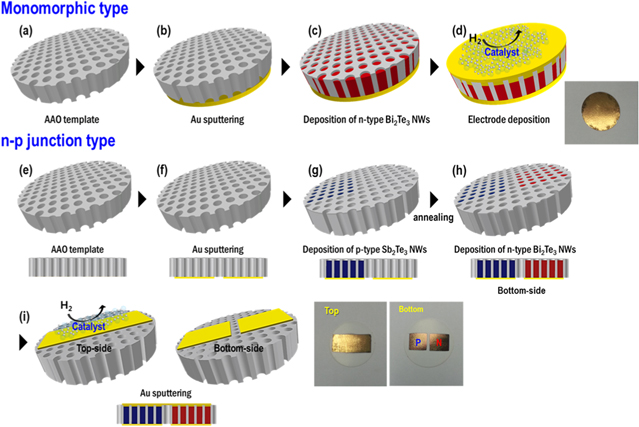
Figure 1. Schematic illustrations of (a)–(d) monomorphic-type and (e)–(i) n–p junction-type thermoelectric layers composed of chalcogenide nanowire arrays synthesized by selective electrochemical deposition into an AAO template.
Download figure:
Standard image High-resolution imageThe second sensor type was an n–p junction-type TCH sensor composed of n-type Bi2Te3 and p-type Sb2Te3 nanowire arrays. Partial masking of the AAO template was required to fabricate this device type; schematic illustrations of the fabrication of n–p junction TE layers by electrochemical deposition into the AAO template are given in figures 1(e)–(i). Two square gold films (total area: 50 mm2) were deposited onto the bottom of the AAO template by means of sputtering (figure 1(f)). The template area over one of these two gold electrodes was sealed with stop-off lacquer (Microstop, Pyramid Plastics, Inc.) and then the template was dried for 1 h in an ambient atmosphere. Then, SbxTe1−x nanowires were deposited into the area over the other gold electrode by electrochemical deposition (figure 1(g)). After deposition, the SbxTe1−x nanowire-deposited AAO template was dipped in acetone to remove the lacquer. And then the device was annealed at 120 °C for 1 h to synthesize the Sb2Te3 phase. Next, the side of the AAO template filled with the SbxTe1−x nanowires was sealed with lacquer, and BixTe1−x nanowires were electrochemically deposited into the open area of the template over the other gold electrode (figure 1(h)). And then a top-side gold nanowire arrays were deposited over both nanowire regions by electrochemical deposition. Finally, gold electrode was deposited using sputter equipment (figure 1(i)).
2.2. Preparation of mesoporous Pt/γ-Al2O3 catalyst
A Pt/γ-Al2O3 catalyst was used to oxidize hydrogen gas on the surface of the devices, thereby providing a heat source that would create a temperature gradient across the TE layer of the devices composed of either n-type only or both n- and p-type chalcogenide nanowire arrays. In other words, the Pt/γ-Al2O3 catalyst responded to hydrogen gas exposure by heating the device, thereby inducing a detectable electric current through the TE nanowire arrays. A catalyst precursor solution of Pt/γ-alumina was prepared by a sol–gel method, using a method based on that reported by Yoldas et al [18]. Aluminum hydroxide was obtained by the hydrolysis of aluminum isopropoxide (AIP, ≥99.9%, Sigma Aldrich) in 90 °C deionized water for 1 h. During this reaction, a condenser was used to prevent loss of the volatile materials from the chemical reactor. Aluminum hydroxide precipitated to the bottom of the reactor after the reaction. To peptize the precipitated aluminum hydroxide, nitric acid (60%, Junsei) was added to adjust the AIP/H2O/HNO3 mole ratio of the solution to 1:100:0.7, and the solution was then stirred at 90 °C for 5 h. The resulting alumina sol was allowed to cool slowly at room temperature and was then dissolved in a solution of H2PtCl (8 wt%, Sigma Aldrich) with additional stirring for 1 h, thereby obtaining a yellowish Pt/γ-Al2O3 precursor solution. This solution was dried at 80 °C for 24 h in an oven to remove water and other volatile components, and then the dried Pt/γ-Al2O3 precursor was deagglomerated by grinding using a mortar. Finally, it was calcined at 600 °C for 1 h to remove the organic additive. Mesoporous alumina was obtained to use as the heating catalyst on TE layer as-fabricated by electrochemical deposition, this synthesis method of mesoporous alumina catalyst has been reported in our previous investigation [19].
3. Results and discussion
3.1. Selection of the lower thermal diffusion layer
The low thermal conductivity of the AAO template was a necessary property for its use as a matrix for synthesizing the one-dimensional TE nanostructures. If the thermal conductivity of the template were greater than that of the TE materials, the performance of the resulting TE device would be worsened due to heat loss by thermal diffusion into the template. The thermal conductivities of the TE materials bismuth telluride (bulk Bi2Te3) and antimony telluride (bulk Sb2Te3) are 1.5 W mK−1 [20] and 1.6 W mK−1 [21], respectively. Therefore, in this system the template must have lower thermal conductivity than these TE materials. A commercially available AAO template with 200 nm pores (Whatman Anodisc 13, Germany) was used to fabricate the TE layer of chalcogenide nanowire arrays; the thermal conductivity of the AAO template was measured by multiplying its specific heat capacity (Сp), density (ρ) and thermal diffusivity (λ) based upon the laser flash method:

The density of gold deposited on the AAO template was measured by Archimedes' principle, yielding the density of 2.683 ± 0.23 g cm−3. Before this measurement, the AAO template was immersed in boiling deionized water at about 100 °C to fill its pores. Specific heat capacity and thermal diffusivity were analyzed at 25 °C by differential scanning calorimetry (DSC, TA instrument, Q200) and LFA (NETZSCH, LFA 447); the measured values were 0.72 ± 0.14 J g−1 °C−1 and 0.54 ± 0.13 mm2 s−1, respectively. Thus, the thermal conductivity of the gold-deposited AAO template with 200 nm pores was determined to be 1.18 ± 0.22 W mK−1 at 300 K. In previous studies, Borca-Tasciuc et al [22] reported the thermal conductivity of the AAO template to be 1.3 W mK−1 at 300 K, and Ogden et al [23] reported values between 0.5 and 1.0 W mK−1; our present results were similar to these results. These results suggest the possibility of a new type of TCH sensor using an AAO template.
3.2. Synthesis of stoichiometric chalcogenide nanowire
Stoichiometry is important and necessary in chemistry because it can dictate the properties of materials, such as their electrical and TE properties [24]. In other words, optimum stoichiometry of a material leads to high performance in terms of its TE properties. The content of Bi deposited in the nanowires was studied as a function of the potential applied during deposition; the Bi content increased from about 36 to 83 at% Bi with increasing negative potential from 0.125 to −0.075 V (figure 2(a)). In this case, the Bi used to form BixTe1−x was strongly influenced by the Bi3+ concentration when compared to the relatively lower HTeO2+ concentration. The stoichiometric composition was realized by deposition under the potential of 0.075 V in an electrolyte containing 0.07 M Bi3+ and 0.01 M HTeO2+ in 1 M HNO3. Like Bi, the deposited Sb content increased from about 4 to 38 at% Sb with increasing negative potential from −0.10 to −0.19 V in an electrolyte containing 0.02 M SbO+, 0.01 M HTeO2+, 0.5 M C4H6O6, and 1 M HNO3(figure 2(b)). In the fabrication of SbxTe1−x nanowires, it was difficult to obtain the stoichiometric composition. To obtain stoichiometric Sb2Te3 nanowires, we annealed nanowires of a near-stoichiometric composition resulting from deposition at an applied voltage of −0.17 V. Annealing was performed at 120 °C for 1 h in atmospheric conditions. The morphology and composition of the Bi2Te3 and Sb2Te3 nanowires were investigated by field emission scanning electron microscopy and energy-dispersive x-ray spectroscopy (EDS). Figures S1(a)–(c) shows cross-sectional images and EDS composition results of Bi2Te3 nanowire arrays synthesized by electrochemical deposition with an applied voltage of 0.075 V. As shown, the BixTe1−x nanowires grew well and with high density, and their composition approached that of the Bi2Te3 phase. Cross-sectional views and EDS composition results of SbxTe1−x nanowire arrays before and after annealing are shown in figures S1(d)–(i). The composition of as-synthesized SbxTe1−x nanowire arrays synthesized with an applied voltage of −0.17 V were revealed to be 26.11% Sb and 73.89% Te. The annealing at 120 °C for 1 h, changed the composition of the SbxTe1−x nanowire arrays to 37.24% Sb and 62.76% Te, which is near stoichiometric. X-ray diffraction (XRD) patterns were obtained for accurate analysis of the phase components and structure of each nanowire. The XRD pattern of the as-synthesized Bi2Te3 nanowires is shown in figure 3(a). All of the detected peaks were indexed to the rhombohedral structure. The XRD pattern of the phase corresponds with that of Bi2Te3 (JCPDS: 00-015-0863), and no other phases existed in the measured product. Annealing effects of SbxTe1−x nanowires were investigated by XRD analysis (figure 3(b)). Before annealing, a SbxTe1−x nanowire was revealed in which Sb0.405Te0.595 (00-045-1228) and Te (00-036-1452) showed a mixed amorphous structure. However, the crystal structure was changed from amorphous to crystalline by annealing, yielding a Sb2Te3 (00-015-0874) phase without other phases such as tellurium. Figures 4 and 5 show HR-TEM and fast Fourier transform (FFT)-converted SAED patterns of a Bi2Te3 nanowire and a Sb2Te3 nanowire, respectively. Actually, it is difficult to analyze the microstructure of a nanowire with the diameter of 200 nm. Therefore, we used nanowires under 200 nm for TEM analysis; these were grown in an AAO template with 100 nm pore diameter by means of electrochemical deposition, yielding as-deposited nanowires 100 nm in diameter (figure 4(a)). FFT-converted SAED patterns confirmed the synthesis of polycrystalline Bi2Te3 nanowires without elemental Bi or Te (figures 4(b)–(f)); FFT patterns of HR-TEM images of these nanowires were consistent with the d-spacing value of the (015), (110), (0, 2, 10) and (205) lattice planes of the rhombohedrally structured Bi2Te3 phase, consistent with XRD results. HR-TEM images and FFT-converted SAED patterns of a Sb2Te3 nanowire after annealing at 120 °C for 1 h are shown in figure 5. The nanowire was synthesized in an AAO template with the pore diameter of 100 nm, the same as that used to fabricate the Bi2Te3 nanowire, and yielding a nanowire 100 nm in diameter, with d-spacing values of the (110), (015) and (0, 0, 18) lattice planes consistent with the rhombohedrally structured Sb2Te3 phase. EDS analysis of the Bi2Te3 and Sb2Te3 nanowires was conducted to confirm their elemental contents. For the Bi2Te3 nanowire 100 nm in diameter, the EDS dot scan profiles showed the Bi/Te atomic ratio of 40.59 ± 0.6 to 59.41 ± 0.6 (figure S2(a)), indicating that the nanowire was composed of the stoichiometric Bi2Te3 phase. EDS dot scan profiles of the Sb2Te3 nanowire showed the Sb/Te atomic ratio of 34.93 ± 1 to 65.07 ± 1 (figure S2(b)), which was within the error detection range of 5% for stoichiometric Sb2Te3. To characterize the semiconducting behavior at the interface between the as-deposited nanowires and the electrolyte, Mott–Schottky measurement was performed [25] by means of an electrochemical workstation operated using the ac impedance method, which can demonstrate the carrier types (hole, p-type or electrons, n-type) and carrier concentrations of nanowire arrays. All these measurements were conducted in a conventional three-electrode system with the AAO template, using the deposited Bi2Te3 and Sb2Te3 nanowire arrays as the working electrode, Ag/AgCl with saturated KCl as a reference electrode and a Pt electrode as a counter electrode. The electrolyte used consisted of 0.1 M NaClO4 and 0.1 M HClO4 in deionized water. The capacitance of the chalcogenide nanowire-containing AAO template/electrolyte system was measured over the ac frequency range of 10–200 kHz with the potential ranging from −0.1 to 0.1 V versus Ag/AgCl at the scan rate of 1 mV s−1. Mott–Schottky plots of the Bi2Te3 and Sb2Te3 nanowire arrays synthesized by electrochemical deposition show positive slopes for the Bi2Te3 nanowire arrays, indicating n-type semiconducting behavior, and negative slopes for the Sb2Te3 nanowire arrays, indicating p-type behavior (figure S3). The average carrier concentrations of the Bi2Te3 and Sb2Te3 nanowires were revealed to be 1.31 × 10²⁰ (±1.03 × 10²⁰) cm−3 and 3.70 × 10²⁰ (±1.96 × 10²⁰) cm−3, respectively; these values are similar to previously reported results [26, 27].

Figure 2. Dependence of the atomic content of (a) Bi in BixTe1–x nanowires (0.07 M Bi3+, 0.01 M HTeO2+, 1 M HNO3) and (b) Sb in SbxTe1−x nanowires (0.02 M SbO+, 0.01 M HTeO2+, 0.5 M C2H4O4, 1 M HNO3) upon the potential applied during potentiostatic deposition using the bath temperature of 25 °C.
Download figure:
Standard image High-resolution image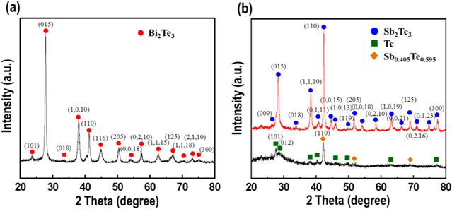
Figure 3. X-ray diffraction patterns of potentiostatically deposited (a) Bi2Te3 and (b) Sb2Te3 nanowire arrays, (black line) before and (red line) after annealing at 120 °C for 1 h.
Download figure:
Standard image High-resolution image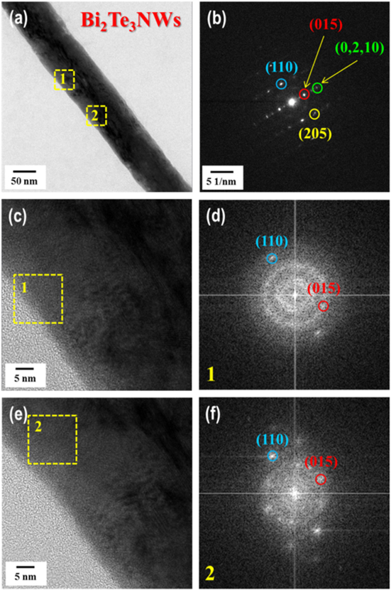
Figure 4. High-resolution TEM images and FFT-converted SAED patterns of a Bi2Te3 nanowire 100 nm in diameter, synthesized by electrochemical deposition.
Download figure:
Standard image High-resolution image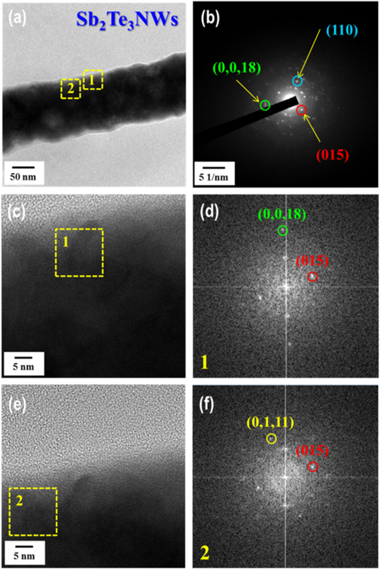
Figure 5. High-resolution TEM images and FFT-converted SAED patterns of a Sb2Te3 nanowire 100 nm in diameter, after annealing at 120 °C for 1 h.
Download figure:
Standard image High-resolution image3.3. Hydrogen gas sensing properties
Sensing properties, including gas detection and response time, were measured using a custom-made apparatus. The output voltage signal of each TCH sensor under test was measured using a nanovoltmeter (2182 A, Keithley) that was placed in contact with the thermochemical sensor. Temperature change due to hydrogen oxidation was monitored by using an IR thermometer (CM sensor, Raytek) located on the top side of the TE layer. As-synthesized 2 vol% mesoporous Pt/Al2O3 catalyst (0.05 g) was placed on top of the TE layer, the nanowire-embedded AAO template. The catalyst played a supporting role in the TCH sensor. The two internal electric wires were made of copper. The release of a H2/air mixture gas for sensing was repeated with regular time interval for 180 s on, 600 s off at fixed a 100 sccm flow rate. Hydrogen sensing properties of the monomorphic-type and n–p junction-type TCH sensors were studied as a function of hydrogen concentration (0.5–5 vol%); for both sensor types, the output voltage signal increased with increasing temperature at the flow rate of 100 sccm (figure 6). For the monomorphic-type TCH sensors, the voltage signal reached 23.7 μV at the hydrogen concentration of 5 vol%, while the n–p junction-type TCH sensor yielded a 215 μV signal at 5 vol%, which is a 9-fold increase compared that of the monomorphic-type TCH sensor. The n–p junction-type TCH sensor was serially connected to n-type and p-type nanowire arrays, which gathered much more output voltage than that of the monomorphic-type TCH sensor under the same temperature gradient. The output voltage profiles were collected for various flow rates (50–300 sccm) of 1% hydrogen gas; like the effect of concentration, the change voltage showed constantly increase with respect to changes in the flow rate of hydrogen. Also, the n–p junction-type TCH sensor was 10.6 times as effective as the monomorphic-type TCH sensor at 1 vol% H2/air (figure 7). For practical applications, the LDL of the hydrogen sensor should be defined. Here, it was determined by using an n–p junction-type TCH sensor to improve the sensitivity under low-temperature conditions. Low-concentration hydrogen detection of the n–p junction-type TCH sensor was studied by plotting its response to various hydrogen concentrations at the constant flow rate of 500 sccm; the sensor was able to detect 400 ppm of hydrogen gas without external interference such as moisture (figure 8).
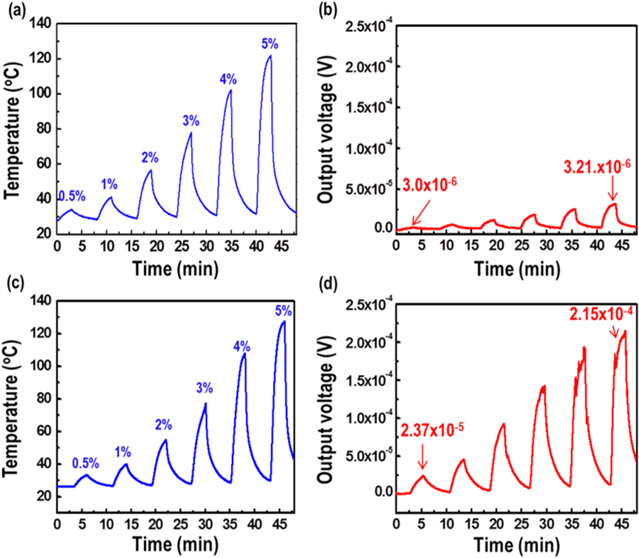
Figure 6. Responses of (a) and (b) monomorphic-type and (c) and (d) n–p junction-type thermochemical hydrogen sensors during exposures to various hydrogen concentrations. The flow rate of hydrogen was fixed at 100 sccm.
Download figure:
Standard image High-resolution image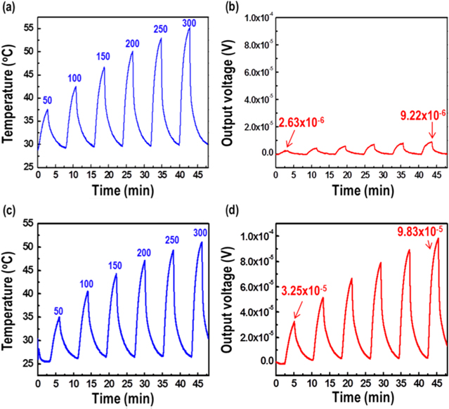
Figure 7. Hydrogen sensing properties of (a) and (b) monomorphic-type and (c) and (d) n–p junction-type thermochemical hydrogen sensors as a function of flow rate. The concentration of hydrogen was fixed at 1 vol%.
Download figure:
Standard image High-resolution image
Figure 8. Low-concentration hydrogen sensing properties of an n–p junction-type thermochemical hydrogen sensor composed of Bi2Te3 and Sb2Te3 nanowire arrays. The flow rate of hydrogen was fixed at 500 sccm.
Download figure:
Standard image High-resolution imageGenerally, the response of TE-type hydrogen sensors is relatively slow compared to that of semiconductor-type hydrogen sensors. Some studies were performed to achieve fast response in TE hydrogen sensors. A response time of 30 s at 3 vol% hydrogen in air was achieved by Luan et al [28], while Nishibori et al achieved an average response time of 2.5 s for 10 000 ppm hydrogen in air by using a Pt catalyst and heating to 100 °C [12]. However, the speed of detecting high concentrations of hydrogen gas at room temperature is still insufficient, and more systematic studies are required for practical applications. Specifically, rapid gas detection at high concentrations is important for practical applications. Output voltage time series of the n–p junction-type TCH sensor in response to hydrogen gas concentrations from 10 to 45 vol% H2/air are shown in figure 9. All experiments were carried out using Pt/Al2O3 catalyst (0.004 g), and included the continuous release of a mixed gas of H2/air for 120 s with a 500 sccm flow rate, which was stopped when voltage signal became saturated. The response times (t90) of TCH sensor with hydrogen concentrations were calculated using this time-dependent voltage signal. It was found that the response time gradually decrease with increasing hydrogen concentration at fixed a 500 sccm flow rate. The upper TE layer was heated by the Pt/Al2O3 catalyst when it reacted with hydrogen, so the reaction with higher concentrations of hydrogen gas increased the output voltage signal of the TCH sensor within a shorter time. In other words, the temperature difference between the upper and lower part of the TCH sensor was reduced by increasing the temperature of upper part resulting in fast voltage saturation due to decline of delta-T (temperature difference) of the TE layer. This allowed fast response by the TCH sensor. Also, for concentrations studied above 30 vol% H2/air, output voltage rapidly decreased and the sensor responded very rapidly. These results are caused by the use of dry air, which contains 79% nitrogen and 21% oxygen, and enables the n–p junction-type TCH sensor to detect the maximum 30 vol% hydrogen because this blend achieves the maximally efficient ratio of 2:1 hydrogen:oxygen. Consequently, rapid response times of TCH sensor were achieved because a small amount of catalyst easily reached the saturation temperature. Further, it is possible to adjust the response time by varying the catalyst amount without requiring the use of another system.

Figure 9. Time-dependent output voltage signal of an n–p junction-type thermoelectric hydrogen sensor composed of Bi2Te3 and Sb2Te3 nanowire arrays exposed to high hydrogen concentrations of (a) 10 vol%, (b) 15 vol%, (c) 20 vol%, (d) 25 vol%, (e) 30 vol%, (f) 35 vol%, (g) 40 vol%, and (h) 45 vol%. The flow rate of hydrogen was fixed at 500 sccm.
Download figure:
Standard image High-resolution image
4. Conclusions
We fabricated a new type of TCH sensor composed of a TE layer of stoichiometric, one-dimensional chalcogenide nanowire arrays, synthesized by electrochemical deposition to embed them into an anodic aluminum oxide (AAO) template, coated with a Pt/γ-Al2O3 catalyst acting as a heating element. In hydrogen sensing tests, the sensor's output voltage increased with increasing temperature upon exposure to hydrogen. Also, the sensor had a wide range of detection (from 400 ppm to 45 vol%) and a fast response time of 1.3 s at 45 vol% H2/air gas at room temperature. The output voltage of n–p junction-type TE hydrogen sensors, which was more than 9 times that of monomorphic-type TCH sensors, results from an n–p junction consisting of two types of nanowire arrays connected in series, i.e., n-type Bi2Te3 and p-type Sb2Te3 nanowires. Consequently, we believe that this type of TCH sensor can be widely used for supersensitive of hydrogen gas detection by employing a large number of inexpensive n–p junction chalcogenide nanowire arrays.
Acknowledgments
This work was supported by a grant from the Fundamental R&D Program for Core Technology of Materials (10050890, Chalcogenide nanostructure-based room-temperature (25 °C) H2 & H2S gas sensors with low power consumption) and The Energy Efficiency & Resources program (20112010100100) and supported by the Industrial Strategic Technology Development Program (10045177, Development of Resistive Ceramic Thin Film using Solution Process and Low Temperature Thin Film Vacuum Getter) funded by the Korea government Ministry of Trade, Industry.