
Abstract
The availability of reliable and well-engineered commercial instruments and data analysis software has led to development in recent years of robust and ergonomic atom-probe tomographs. Indeed, atom-probe tomography (APT) is now being applied to a broader range of materials classes that involve highly important scientific and technological problems in materials science and engineering. Dual-beam focused-ion beam microscopy and its application to the fabrication of APT microtip specimens have dramatically improved the ability to probe a variety of systems. However, the sample preparation is still challenging especially for emerging nanomaterials such as epitaxial nanowires which typically grow vertically on a substrate through metal-catalyzed vapor phase epitaxy. The size, morphology, density, and sensitivity to radiation damage are the most influential parameters in the preparation of nanowire specimens for APT. In this paper, we describe a step-by-step process methodology to allow a precisely controlled, damage-free transfer of individual, short silicon nanowires onto atom probe microposts. Starting with a dense array of tiny nanowires and using focused ion beam, we employed a sequence of protective layers and markers to identify the nanowire to be transferred and probed while protecting it against Ga ions during lift-off processing and tip sharpening. Based on this approach, high-quality three-dimensional atom-by-atom maps of single aluminum-catalyzed silicon nanowires are obtained using a highly focused ultraviolet laser-assisted local electrode atom probe tomograph.
Export citation and abstract BibTeX RIS
1. Introduction
Atom-probe tomography (APT) is an analytical technique that provides a three-dimensional (3D) view of the internal structure of nanoscale materials with a near atomic spatial resolution [1–5]. A 3D atom-probe tomograph combines a field-ion microscope with a special time-of-flight (TOF) mass spectrometer. The ability to determine the TOFs of individual ions allows establishing their mass-to-charge (m/n) ratios and hence their chemical identities. This is followed by reconstruction in 3D of a given volume of material using proper software programs. Recent years have known the development and commercialization of the sophisticated local electrode atom-probe (LEAP) tomographs [6–10], which enable the application of APT to a broader range of materials classes that involve highly important scientific and technological problems in materials physics and engineering. For example, APT is being employed to investigate heretofore unexplored problems concerning metallic structural materials, semiconductor thin films and nanomaterials, metal oxides, organic/inorganic interfaces, and organic and biological materials (for a review see [2]).
The key step in APT analysis remains the preparation of needle-shaped specimens. Although the preparation process is well-established for thin films and bulk materials [1], it remains highly challenging for nanoscale materials and devices. In this manuscript, we describe a step-by-step procedure to achieve a precisely controlled, damage-free transfer of individual semiconductor nanowires onto microtips for LEAP analysis. Semiconductor nanowires are quasi-one-dimensional nanostructures that have been attracting a great deal of interest as versatile building blocks for innovative nanoscale devices enabling a vast variety of applications in nanoelectronics, biosensing, and environment-friendly energy conversion [11]. These emerging nanotechnologies exploit size-related effects, the flexibility in the fabrication and design offered by the use of nanowires and the concomitant progress in probing nanoscale properties. Besides their technological importance, nanowires also provide a rich playground to explore the basic properties of important semiconductors on the quantum and nanometer scales. A precise probe of the composition of a nanowire is thus of paramount importance in these studies and applications. Transmission electron microscopy-based techniques are widely employed to serve this purpose. These techniques provide inarguably the highest spatial resolution. However, they are unable to resolve elements having close atomic numbers and their 3D imaging capabilities remain limited. Additionally, the state-of-the-art energy dispersive x-ray spectroscopy requires concentrations that are typically higher than ∼0.5 at%. Because of its superior detection sensitivity of <10 atomic ppm with a near atomic-scale spatial resolution, APT can be employed to achieve a more accurate and rigorous analysis of the composition of semiconductor nanowires.
2. Experimental details
In these studies, we utilized Northwestern University's UV laser-assisted LEAP tomograph (LEAP 4000XSi (Cameca, Madison, WI)). Pulsed-evaporation of individual atoms is achieved employing a focused picosecond UV (λ = 355 nm) laser with a laser beam waist of <5 μm at the e−2 diameter. The pulse repetition rate is variable in steps from 1 to 500 kHz and a detection rate of up to 5 × 10⁶ ions min−1 can be obtained. The maximum cross-sectional area of a microtip specimen analyzed can be 200 nm × 200 nm, at the minimum distance of a microtip from the MCP. Thus, the system is capable of examining the total cross-sectional area of a single nanowire.
The nanowires investigated in this work are aluminum-catalyzed silicon nanowires. The nanowire growth was accomplished by using monosilane, SiH4, (diluted to 5% in argon) as a precursor at a substrate temperature of ∼410 °C [12–14]. The partial pressure of the monosilane was held below 0.15 mbar during growth. Under these conditions, the grown nanowires have a length of ∼(241 ± 15) nm and a diameter of ∼(37 ± 11) nm (figure 2(a)). Although the temperature used is below the aluminum–silicon macroscopic eutectic temperature [15], the growth is believed to occur via the classical vapor–liquid–solid mechanism involving undercooled aluminum–silicon nanodroplets. For the preparation of nanowire LEAP specimens, we have developed a focused ion beam- (FIB-) based damage-free process methodology to attach individual nanowires to the commercially available silicon microposts (figure 1). A step-by-step description of this preparation process is provided in the following section.
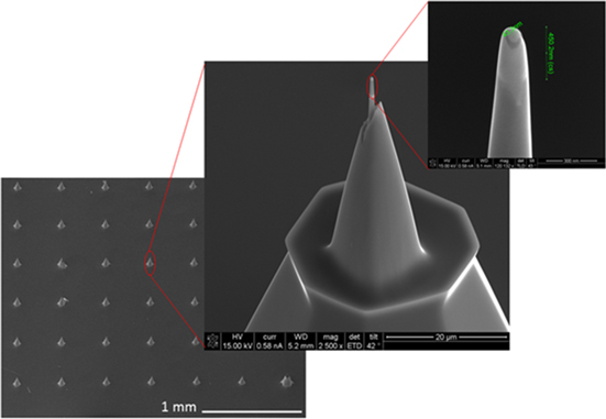
Figure 1. SEM image of an array of silicon microposts used for APT analyses of silicon nanowires. The close-up images show a single nanowire attached on the top of a micro-post. The nanowire is located in the bright region at the tip apex. The nanowire is capped by a Ni protective layer and the attachment was achieved using FIB processing as described in the text.
Download figure:
Standard image High-resolution imageFIB processing was conducted in a FEI dual-beam Nova Nanolab 600 SEM/FIB. The silicon microtips were subsequently inserted into the LEAP tomograph's ultrahigh-vacuum chamber and cooled to 60 K prior to pulsed UV laser-assisted evaporation analyses. The evaporation rate (ion pulse−1), the laser pulse repetition-rate, and energy pulse−1 were 0.01, 500 kHz, and 40 pJ, respectively. The use of a highly focused UV laser beam decreases local heating, thereby improving the detection limits and mass resolving power (m/Δm), where m is the mass of an isotope [16]. The 3D reconstructions and statistical analysis of concentration frequency were performed using Cameca's IVAS program.
3. Preparation of LEAP nanowire specimens
A few successful examples of LEAP 3D imaging of single nanowires were recently demonstrated [17–25]. Two methods were mainly employed to prepare nanowire specimens, namely, direct growth of nanowires on silicon microtips [17–20] and the pluck-and-place approach [23–25]. In the latter, a micromanipulator is employed to detach nanowires from the growth substrate and transfer them to silicon microtips. Our tests employing this method have indicated that the use of a micromanipulator to pluck-and-place nanowires is very sensitive to vibrations and can only be effective for nanowires with sufficiently high aspect ratios. The method of direct growth of nanowires on APT microtips is very laborious and requires a substantial number of trials in order to find a well positioned nanowire. To circumvent all of these difficulties, we developed a reliable methodology process to transfer individual very thin and short nanowires using FIB nanomachining. FIB processing is an ideal tool to prepare APT specimens provided that the sample is properly protected against Ga ion-induced damage. For bulk materials or thin films that are sufficiently thicker than the damaged layer (typically ∼20 nm), needle-like specimens can easily be engineered by FIB following a circular milling procedure even without prior deposition of protective layers [26, 27]. For these samples often the APT data of the topmost damaged layers are not of interest and simply omitted in the analysis. However, radiation damage cannot be tolerated in nanoscale structures such as nanowires, which can be easily amorphized or severely contaminated during the preparation. Therefore, developing a damage-free FIB processing is highly critical to achieve a reliable 3D mapping of semiconductor nanostructures.
In order to optimize the FIB preparation, we first performed detailed simulations of Ga-ion induced damage in silicon nanowires using SRIM program [28]. The ion energy used in these simulations is 30 keV under the two different configurations of normal and 88° incidences thus mimicking the conditions used in typical FIB processing. The nature and the thickness of the protective layer were also considered in these simulations. The calculated profiles clearly show that a 40 nm thick Ni layer is effective in protecting silicon nanowire from radiation damage. The use of epoxy instead of Ni as a capping layer leads to Ga implantation in silicon nanowires. Note that FIB-deposited Pt layers were also explored. Although they can limit the nanowire damage, APT analysis using nanowires capped with these layers has always failed. In fact, this electron beam deposited Pt is in reality a composite of mainly carbon and small Pt crystallites with less than 20% Pt content, and during the circular milling these Pt layers are preferentially etched. Moreover the electrical conductivity of this layer is rather small which has led to a systematic breaking of the tip once subjected to the strong electrical field during the APT measurement. Consequently, we decided to use pure Ni as a first protection layer. Moreover, Ni also acts as an excellent marker in the APT analysis as Ni atoms are detected with a very clear signal. In an early study [29], Ni was also employed as a protection layer during the FIB transfer of single several microns long nanowires. In that work, Ni was removed chemically prior to APT analysis. This approach cannot, however, be extended to samples with high density of tiny nanowires. In the following, we outline the multi-step FIB preparation to transfer individual nanowires on silicon microtips.
The first step in nanowire specimens' preparation consists of the deposition of a uniform shell of Ni around silicon nanowires. Based on Monte Carlo simulations, a 40 nm thick Ni protective layer was deposited to prevent Ga ions from reaching silicon (figure 2(b)). The deposition was performed by a Gatan ion sputtering machine (PECS) were a Ni target is irradiated by 10 keV Ar ions and the sputtered atoms slowly form a complete layer uniformly capping the nanowires. The thickness of the deposited Ni layers was continuously verified using SEM measurements. The estimated Ni deposition rate is about 1 nm s−1. After Ni deposition, the remaining free space between the Ni-capped nanowires was filled by an ion beam-deposited Pt layer to form a 1 × 7 μm2 area just as used in case of TEM lamella preparation. The thickness of the layer was adjusted to about 500 nm such as the nanowires can still be distinguished in SEM images (figure 2(c)). Subsequently, a set of aligned individual nanowires (typically 3–8 nanowires) separated by ∼2.5 μm are selected and each of them was marked by a circular 500 nm thick Pt pad with 1 μm in diameter with a central hole exactly at the selected nanowire position (figure 2(d)). As described below, such markers have a good contrast in ion beam SEM image and remain stable throughout the following steps thus enabling the visual control needed to correct for any possible drift during FIB processing. Figures 2(e) and (f) display the fabrication of a lamella with preselected three nanowires. This step corresponds to the usual preparation of TEM lamellae. Between two vertical pits at both sides of the Pt layer a 1 μm wide bar is defined, which after a 'U' cut is lifted out using the Omniprobe micromanipulator onto which the bar is welded by ion beam assisted deposition of Pt.
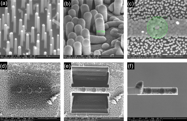
Figure 2. SEM images of FIB processing for nanowires LEAP specimens. (a) As-grown aluminum-catalyzed silicon nanowires. (b) Ni-capped as-grown nanowires. The Ni layer thickness is ∼40 nm. (c) Nanowire sample after FIB deposition of an additional Pt protection layer. (d) Deposition of circular markers each centered on a single nanowire for subsequent fine positioning of a milling pattern. (e) Coarse milling by the common FIB TEM process. (f) Lift-out of a lamella with three pre-defined nanowire specimens.
Download figure:
Standard image High-resolution imageOnce the bar with the embedded nanowires has been lifted out, segments of the bar containing one pre-selected nanowire each are transferred one by one onto the previously FIB-modified APT microposts (figures 3(a) and (b)) using a piecemeal glue and cut procedure. First the front segment of the bar with one nanowire is fixed onto the microtip by two small Pt patches. The process is repeated until all segments are attached to microtips. After fixing all the pieces at the posts it is important to fill up the empty space below the pieces completely with additional Pt as the initially deposited side patches will be milled off during the following cylindrical milling to reduce the diameter of the pillars (figures 3(c) and (d)). To precisely form cylindrical pillars, the pre-defined ring-shaped milling routines of the FIB are used which allow free variation of the outer and inner radius of the milling area. The outer radius should be set in the beginning at least to 4 or 5 μm to avoid the formation of sharp circular ridges close to the central region of the microtip. Finally, pillars with a diameter of ∼1 μm and a height of ∼10 μm each containing one preselected silicon nanowire are obtained (figure 3(d)). The nanowire to be probed is positioned just below the central hole of the marker. Ideally, this hole should be accurately centered and the pillar sidewalls should be aligned with the sidewalls of the supporting micropost. Particularly, the apex of the pillar has to be adjusted to form a tip with diameter below 100 nm while keeping the Ni-capped preselected nanowire at the center of the tip (figures 3(e) and (f)). Here, the circular milling procedure at 30 kV ion beam energy was applied. The ion beam live monitor image of the marker's hole enables centering the milling pattern directly onto the position of the buried nanowire. This allows to manually compensate for lateral drifts by the electrical fine shift controls. Gradually, the circular Pt marker will be removed during this process. The control of the tip symmetry is achieved by secondary electron imaging of the sidewalls where the Ni cap layer becomes visible when Pt is milled off. Even at the lowest possible ion beam current (1.5 pA at 30 kV) the milling of the tips would be very fast, thus one has to reduce the local ion dose by choosing a quite large outer diameter of the circular milling pattern to be able to control the process. At the end of this process, the Pt protection layers should be milled off, whereas the Ni is preserved to a large extent. Alternatively, once the pillar has been shaped to an intermediate state (figure 3(d)), the final preparation step can be performed by a simple low kV, large area milling. Indeed, a broad 5 kV or 2 kV ion beam with perpendicular incidence produces, in a very short time and without any adjustments, a very sharp tip while keeping the preselected nanowire at the center of the tip. An additional advantage is that this low-energy milling leaves only a very thin damage layer of few nm. However, if the targeted nanowire is only slightly out of the pillar center of the starting pillar, there is no way to correct or readjust its position at this stage.

Figure 3. SEM images of the process of nanowire transfer onto a silicon micropost for LEAP analysis. (a) Transfer of a lamella segment to the FIB-modified APT micropost. (b) Repeated Pt glue and cut to attach a segment containing a single marked nanowire. (c) Coarse milling of circular pillar around the marked nanowire. (d) Close-up image of a pillar containing several silicon nanowires partly visible at the edge, but the nanowire to be probed is located just below the central hole. (e) Fine milling of a sharp tip (radius < 40 nm) containing one nanowire capped with Ni and Pt layers. (f) Final tip ready for LEAP measurement. The bright contrast corresponds to the Ni protective layer.
Download figure:
Standard image High-resolution image4. 3D atom-by-atom mapping of single nanowires
Using the methodology process described in the previous section, successful APT analyses of individual aluminum-catalyzed silicon nanowires was achieved using UV-LEAP. Figure 4 displays a representative mass spectrum recorded during a typical LEAP analysis. Despite the very close atomic masses of aluminum and silicon, peaks associated with these two elements are well resolved in the mass spectrum. A 3D atom-by-atom map of a single nanowire covered by a protective Ni layer is shown in figure 5(a). The figure also displays the 3D distribution of Ga atoms during FIB processing (figures 5(b) and (c)). It is important to note that Ga atoms are predominantly (>99.95 at%) confined in the Ni protective layer. Achieving APT analysis for nanowires provides valuable insights into their structure and composition. For instance, the nature and distribution of impurities within a tiny system such as a nanowire can be quantitatively obtained as demonstrated in figure 6. This figure displays the concentration of aluminum in a silicon nanowire (figure 6(a)) as well as the profiles of aluminum and silicon in a catalyst nanoparticle (figure 6(b)). Interestingly, the average aluminum concentration measured in the investigated silicon nanowires is ∼(2.0 ± 0.5) × 1020 atom cm−3 (∼0.4 at%). Strikingly, this is about four orders of magnitudes greater than the extrapolated equilibrium solubility of aluminum in silicon. Based on APT data, the underlying physics of this phenomenon of catalyst atom incorporation in nanowires is addressed in details in [12].
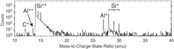
Figure 4. A representative mass spectrum recorded during LEAP analysis of a single as grown aluminum-catalyzed silicon nanowire. Peaks associated with silicon and aluminum are indicated. Note the logarithmic vertical scale.
Download figure:
Standard image High-resolution image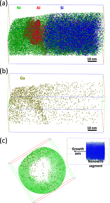
Figure 5. (a) 3D APT atom-by-atom map of a nanowire grown at 410 °C. For the sake of clarity only a limited number of atoms is displayed (2.5 × 10⁴ atoms of each element). (b) 3D distribution of Ga atoms introduced during the FIB preparation. More than 99.95% of Ga atoms are confined in the Ni layer. (c) View along the growth axis of a segment of the nanowire (inset) showing the distribution of Ni and Ga atoms.
Download figure:
Standard image High-resolution image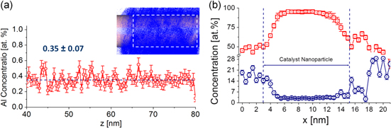
Figure 6. (a) Aluminum axial concentration-profile in a single nanowire measured for a cylindrical segment with a diameter of 20 nm. The horizontal dashed line denotes the average concentration, 0.35 ± 0.07, and error bars represent ±1s.d. The number of Al atoms in the sampling volumes varies between ∼2000 and 4500. (b) Radial concentration profiles of Al and Si in the catalyst nanoparticle. The error bars present the standard deviation calculated for the analyzed volume containing 2.9 × 10⁵ Al atoms and 8 × 10³ Si atoms.
Download figure:
Standard image High-resolution imageTo quantitatively address the distribution of aluminum atoms in silicon nanowires, APT 3D maps provide the possibility to perform detailed statistical analysis of catalyst atoms spatial distribution in individual silicon nanowires. We defined arbitrarily spherical volumes with a diameter d in a single nanowire and counted the number of aluminum atoms within each sphere using the IVAS program. The process was repeated for about a hundred times for two sets at d = 0.6 and 0.8 nm. The results of our statistical analysis are displayed in figure 7(a) and demonstrate that aluminum does not form clusters in silicon nanowires. Thus, despite the sizable amount of aluminum detected in the nanowire, aluminum clusters and precipitates do not form. Impurity clustering can also be studied through statistical analyses of the spatial distribution of aluminum atoms and partial aluminum–aluminum radial distribution function [30, 31]. The binomial analysis was performed with sampling blocks of 200 atoms. The entire volume is first divided into columns along the z-axis, with a cross-section in x- and y- directions, so that the volume dxdydz contains 200 atoms on average. For obtaining blocks with exactly 200 atoms, each column with cross-section dxdy is then cut into sections with 200 atoms as dz is varied. Example of statistical analysis of concentration frequency is displayed in figure 7(b). This analysis shows that the concentration frequency distribution is not different from a binomial distribution [31] with the same mean at 99% confidence and thus confirms that aluminum does not form clusters in silicon nanowires.

Figure 7. (a) Histograms of the statistical analysis of aluminum catalyst clustering in a silicon nanowire. (b) Results of statistical analysis of aluminum concentration frequency (histogram) and of binomial analysis (solid line). The binomial analysis was performed by sampling blocks containing 200 atoms.
Download figure:
Standard image High-resolution image
5. Conclusion
APT is a powerful tool to analyze the emerging nanomaterials with an unprecedented sensitivity and a near-atomic resolution. The major challenge to achieve 3D atom-by-atom mapping of these systems remains the difficulty in specimen preparation. In this work, we provide a step-by-step description of a methodology process to fabricate APT specimens from high density, thin, and short semiconductor nanowires. Using FIB nanomachining, we introduced a sequence of protective layers and markers to identify the nanowire to be transferred and probed while protecting it against Ga ions during lift-off processing and tip sharpening. Based on this approach, high-quality 3D atom-by-atom maps of single aluminum-catalyzed silicon nanowires are obtained using a highly focused ultraviolet laser-assisted local electrode atom probe tomograph. The developed approach can be employed for a variety of nanoscale materials and devices for a controlled preparation of APT specimens.
Acknowledgement
OM acknowledges support from NSERC, the Canada Research Chair, and Ecole Polytechnique de Montreal (PIED). The LEAP tomograph at NUCAPT was purchased and upgraded with funding from NSF-MRI (DMR-0420532) and ONR-DURIP (N00014-0400798, N00014-0910781) grants. Instrumentation at NUCAPT was supported by the Initiative for Sustainability and Energy at Northwestern. This research made use of the Shared Facilities at the Materials Research Center, supported by the NSF's MRSEC program (DMR-0520513 and 1121262).