
Abstract
One-dimensional Sn-3.5Ag alloy nanosolders have been successfully fabricated by a dc electrodeposition technique into nanoporous templates, and their soldering quality has been demonstrated in nanoscale electrical welding for the first time, which indicates that they can easily form remarkably reliable conductive joints. The electrical measurement shows that individual 1D Sn-3.5Ag nanosolders have a resistivity of 28.9 μΩ·cm. The morphology, crystal structure and chemistry of these nanosolders have been characterized at the nanoscale. It is found that individual 1D Sn-3.5Ag alloy nanosolders have a continuous morphology and smooth surface. XPS confirms the presence of tin and silver with a mass ratio of 96.54:3.46, and EDX elemental mappings clearly reveal that the Sn and Ag elements have a uniform distribution. Coveragent beam electron diffractions verify that the crystal phases of individual 1D Sn-3.5Ag alloy nanosolders consist of matrix β-Sn and the intermetallic compound Ag3Sn. The reflow experiments reveal that the eutectic composition of the 1D Sn-Ag alloy nanowire is shifted to the Sn rich corner. This work may contribute one of the most important tin-based alloy nanosolders for future nanoscale welding techniques, which are believed to have broad applications in nanotechnology and the future nano-industry.
Export citation and abstract BibTeX RIS
1. Introduction
Individual nanoobjects, such as nanoparticles, nanowires and nanotubes, can now be routinely fabricated by a number of physical, chemical and biological methods. An urgent task and one of the central challenges for the realisation of practical applications in nanotechnology is the development of reliable routes to construct and integrate these nanoobject building blocks into nanoscale systems because secure, functional and long-lasting bonds are a necessity for devices with a long lifetime. Bonding techniques that work on individual nanomaterials or nanounits at the nanoscale have lagged behind and become a bottleneck, obstructing the fabrication of diverse nanoeletronics and nanosensors that use various nanoobject building blocks, in comparison with nanomaterials' synthesis and self-assembly techniques, which are relatively mature [1–5]. Nanowelding techniques, including electrical nanowelding [6], cold welding [7], ion beam deposition of material [8], laser heating [9], ultrasonic irradiation [10], high-energy electron beam bombardment [11] and electrical Joule heating [12], provide the reality of developing a novel basis of 3D nanoscale fabrication lines for the exploitation of prototype nanoelectronics, nanosensors and nanodevices [1, 2, 13]. High-quality nanosolders are one of the most key factors in determining the success of forming reliable nanobondings, which serve the same roles of traditional solders in various macro- and microscale welding techniques.
The reported nanosolders can be roughly classified into two main groups according to their applications: nanoparticle-doped solders and nanoscale solders. Nanoparticle-doped solders are prepared by mixing various nanoparticles into traditional solders, solder pastes, soldering lugs and welding rods. After lead was banned from use as an elemental composition in the electronic industry on 1 July 2006 due to its high toxicity and environmental pollution [14], doped nanoparticles have mainly been used to improve the qualities of conventional solders, including their good solderability, low surface tension, high ductility, good wettability, good electrical properties, low melting temperature and corrosion resistance. So far, various nanoparticles, such as Ni, Cu, Ag, Co, TiO2, Al2O3, ZrO2, SiC, Cu6Sn5, Ni3Sn4, carbon nanotubes, and so on, have been applied into conventional solders [15]. Most of the literature named these nanoparticle-doped solders as nanosolders. However, these solders are still applied in conventional welding technologies from macro- to microscale size because their own sizes are typically larger than 100 nm. To the best of the authors' knowledge, there has thus far been no report on the application of nanoparticle-doped solders into welding nanobuilding blocks or nanopatterns at the <100 nm nanoscale. The fundamental reason for this is believed to be due to the size mismatches among the nanoparticle-doped solders, nanobuilding blocks and welding equipment.
Nanoscale solders means that their size is on the nanoscale (smaller than 100 nm) in at least one of their characteristic dimensions. Diverse nanoscale solders, including 0-dimensional (0D) particles of Sn [16], Sn-Ag-Cu [17], Sn-57Bi, Sn-Ag [18, 19], Sn-0.7Cu-0.4Co, Sn-3.8Ag-0.7Cu [20], Sn-3.5Ag-0.5Cu nanoparticles [21] and 1-dimensional (1D) wires of Sn nanowire, Sn/Ag alloy nanowires [22], Sn/Ag/Cu alloy nanowires [23], Sn99Au1 alloy nanowires [6], Au-Sn/Ag, Au-Cu-Sn, Au-Ni-In and Sn-Ni-Au-Ni-Sn multi-segmented nanowires [24], have been prepared. These 0D nanoparticles have been further developed into nano-solder pastes, which are still applied in macro- and microscale electronic interconnecting functions. The majority of the cited work focuses on the preparation and the morphological, structural and thermal properties of 1D nanowire solders. The application of individual 1D nanosolders into welding nanobuilding blocks and nanopatterns at the <100 nm nanoscale has been surprisingly lacking—except in our previous reports [6]. This is believed to be because the application of individual nanosolders at the nanoscale involves the precise manipulation of nano-building blocks and nanosolders, the simultaneous and dynamical monitoring of whole processes and the reliable controllability of nanowelding and of a high-vacuum environment, all of which exceptionally increase the difficulites of experimental technologies.
Sn-Ag [18, 19] is one group of commerical solders with significant material qualities, such as ductility, creep resistance, thermal resistance and the ability to remain high levels of brightness, which have been widely used in the applications of high temperature, high reliability interconnects, including electronic assemblies, die attachments, central heating, jewelry soldering and hot water pipe welding. They are especially irreplacable in soldering applications in which lead usage is prohibitive, such as in pipe joints that come into contact with water and/or foodstuffs [19]. Their typical composition contain 3–5% silver. Microscale and nanoscale Sn-Ag particles are often commercially availalable [18, 19]. However, they are still applied in conventional welding technologies. There are a lack of reports about the applications of 0D or 1D Sn-Ag nanosolders at nanoscale size.
In this work, we develop a novel 1D Sn-Ag alloy nanosolder fabricated by a dc electrodeposition technique using anodic aluminum oxide (AAO) and polycarbonate (PC) templates. The morphological, structural and chemical characterizations of 1D Sn-Ag alloy nanosolder have been systemically investigated. The quality of 1D Sn-Ag alloy nanosolder has been tested through a range of practical applications in nanoscale nanowelding. We believe that our work contributes an important nanosolder for the future nanoindustry and provides the first step toward the establishment of a future 3D nanoscale fabrication line. It is also significant for the current and future bottom-up localized assembly and for the integration and repair of micro/nanodevices, nanoelectronics, nanosensors and nanoelectromechnical systems.
2. Experimental section
2.1. Preparation of 1D SnAg alloy nanosolder
The Sn-Ag alloy nanowire solders were fabricated by dc electrodeposition into AAO and PC templates with about 50 nm diameter pores. The AAO templates were fabricated by anodizing 99.999% pure Al sheets in a 0.6 M oxalic acid electrolyte for 12 h at room temperature with continuous stirring. An amalgamation process was adopted to peel off the Al substrates. The peeled AAO templates were then immersed into 0.5 M phosphoric acid for 90 min to remove the barrier layers. A gold film (approximately 50 nm thick) that served as a working electrode was evaporated onto one side of the non-barrier layer AAO template. The electrodeposition was achieved in a three-electrode glass cell on a CHI630B electrochemical workstation at room temperature in which the reference electrode was a saturated calomel electrode (SCE), and the counter electrode was a platinum plate. The electrodeposition electrolyte is composed of 0.30 M Sn(CH3SO3)2, 4.5 mM AgI, 0.60 M K4P2O7, 1.0 M KI, 0.4 M TEA, 6.4 mM heliotropin (HT) and 2 g L−1 hydroquinone. The K4P2O7 is a complexing agent for Sn2+ and is also used to prevent Sn2+ hydrolysis and oxidation. The KI is a complexing agent for Ag+, which contributes to the success of the co-deposition of Sn and Ag, inhibiting the replacement between Sn and Ag. Both K4P2O7 and KI also act as a conductive salt, which increases the conductivity of the plating solution. The TEA acts as an assistant brightener and can decrease cathodic polarization. The HT is a main brightener, and the hydroquinone is an antioxidant. The pH value of the electrodeposition electrolyte was adjusted to 5.5–6.0 by adding methanesulfonic acid. The voltammetric experiments (figure 1(a)) in which a Cu sheet was used as a working electrode were completed to determine the optimal electrodeposition potentials for the co-electrodeposition SnAg alloy. When the potential was swept to negative values, two cathodic peaks were observed at −0.606 V and −0.932 V. An EDX quantification analysis revealed that the atomic weight ratios of Sn and Ag at −0.606 V, −0.77 V and −0.932 V potential were approximately 4.5:95.5, 18:82 and 95.7:4.3, respectively; this indicates that peak A is the initial codeposition stage of the Sn-Ag alloy, and the Ag content within the Sn-Ag alloy decreases as the cathodic potential becomes increasingly negative. In this work, a −1.1 V potential was applied to obtain 1D Sn-3.5Ag alloy nanosolders, of which a typical curve of the time dependence of the observed current during the growth of Sn-3.5Ag alloy nanowires in an AAO template is shown in figure 1(b). The typical deposition time for each specimen was set to 30 min, and the electrodeposition electrolyte was continuously agitated throughout by a magnetic stirrer.

Figure 1. (a) A representative CV curve of Sn-Ag electrodeposited from weakly acidic baths containing 0.30 M Sn(CH3SO3)2, 4.5 mM AgI, 0.60 M K4P2O7, 1.0 M KI, 0.225 M TEA, 6.4 mM heliotropin (HT) and 2 g L−1 hydroquinone at a scan rate of 50 mV s−1; (b) A typical curve of the time dependence of the applied deposition potential vs. the SCE during the growth of the 1D Sn-3.5Ag nanosolders; (c) SEM image of bundles of nanosolders, of which AAO templates have been fully dissolved. Inset: top-view and cross-sectional SEM images of an AAO template; (d) SEM image of bundles of 1D Sn-3.5Ag nanosolders fabricated by PC templates; (e) HAADF-STEM image of 1D Sn-Ag nanosolders dissolved from AAO templates. Inset: magnified view of one nanosolder; (f) HAADF-STEM image of 1D Sn-Ag nanosolders dissolved from PC templates.
Download figure:
Standard image High-resolution image2.2. Characterization
The morphological, crystal structural and chemical characterisations of 1D SnAg nanosolder were analyzed at the nanoscale using field emission scanning electron microscopy (FESEM, Hitachi S-4800 II, Japan), a high-resolution transmission electron microscope (HRTEM, TecnaiTM G2 F30, FEI, US) equipped with energy-dispersive x-ray analysis (EDAX, AMETEK Co., LTD), high-angle annular dark-field and scanning transmission electron microscopy (HAADF-STEM) and x-ray photoelectron spectroscopy (XPS, Kratos Axis Ultra DLD, Japan). The AAO templates or PC templates were completely dissolved in a 0.1 M sodium hydroxide solution or in dichloromethane to release the nanowires, which were then rinsed with distilled water and dispersed on Si wafers and holey carbon-coated gold grids for SEM, TEM, STEM, EDX and XPS analysis.
2.3. Welding performance test
The quality tests performed by applying individual 1D SnAg nanosolders into welding nanopatterns at nanoscale size were carried out using two in situ SEM nanomanipulators (Kleindiek Nanotechnik, Germany) equipped with nichrome nanoprobes/nanotips and a Keithley 6487 picoammeter. The data acquisition and nanowelding signal were automated using a dedicated multifunctional program.
2.4. Reflow performance test
The nanowire solder reflow experiments were carried out in a programmable high-temperature tube furnace using the standard industrial reflow profile strategy, which includes preheating, a thermal soak, reflow and cooling steps. The solder nanowires were dropped onto Si wafers and holey carbon-coated copper grids. A glass of no-clean liquid soldering flux was used to clean up the surface oxides of the nanosolders during the reflow experiments, which were placed to the nearby 1D Sn-3.5Ag nanosolders. Nitrogen purging was used to avoid further oxidation of the nanosolders during this process. The temperature was firstly increased to the approximate range of 150–180 °C for 5 min to preheat the wires; then, the temperature was briefly raised to 240 °C for 5 min to ensure a complete reflow. The Si wafer was then brought out of the furnace and cooled down to room temperature.
3. Results and discussion
3.1. Electrode behavior and nanowire morphologies
The morphologies of 1D Sn-3.5Ag nanosolders were observed by SEM and HAADF-STEM. Figure 1(c) shows a representative SEM image of a bundle of flower-like SnAg solder nanowires sticking to a gold template replica at the end, from which the AAO template have been completely dissolved. One can see that the individual SnAg nanowires have a continuous structure and virtually uniform diameter. The size statistics reveal that the average diameter of the prepared SnAg nanowires is approximately 50 nm, which corresponds to the pore diameter of AAO templates, as shown in the inset of figure 1(c). The average length for most of the nanowires is around 10 μm. As shown in figure 1(b), the time of the nanowire growth in the pores (the stable stage) is approximately 1500 s; so, the growth rate of the SnAg nanowires is estimated to be 6.7 nm s−1.
Figure 1(e) shows a representative HAADF-STEM image. The contrast of incoherent high-resolution HAADF-STEM images directly depends on the atomic number and thickness of the materials; in the nanowire images, the SnAg nanowires show a continuous structure and uniform size, which is in agreement with the SEM observation. Their surfaces are smooth and do not show obvious defects, revealing good quality. The magnified HAADF-STEM image (inset of figure 1(e)) shows that individual SnAg nanowires have an even contrast, revealing an even chemical composition along the nanowire's length. Figure 1(d) shows a representative SEM image of a field of wheat-like Sn-Ag nanowires prepared from PC template. The magnified HAADF-STEM image (figure 1(f)) shows that individual SnAg nanowires have uneven diameter-like cylinders. The size statistics reveal that the top diameter is approximately 50 nm, and the bottom diameter is approximately 120 nm. The average length for most of the nanowires is around 5 μm.
3.2. Nanosolder welding performance test
Individual SnAg nanowires have been used in the application of welding nanopatterns at the nanoscale to test their quality as nanosolder. Figure 2 illustrates the whole process. Two gold nanowires that are 55 nm in diameter and about 6 um in length were mechanically manipulated and assembled into a simple nano-pattern such as Chinese number eight '八' on a SiO2(100 nm)/Si wafer; then, a sacrificial Sn-3.5Ag nanowire 100 nm in diameter and 2 um in length, which was used as nanosolder (figure 2(a)), was placed onto the assembled '八' nanopattern at the weld point, as shown in figure 2(b). Before welding, the resistance of the assembled nanostructure was measured as isolating due to the structural disconnection.

Figure 2. Nanowelding two 50 nm gold nanowires using a sacrificial 1D Sn-3.5Ag nanosolder. (a) Release of a Sn-3.5Ag solder nanowire from a Si/SiO2(100 nm) wafer using a nanomanipulator probe to mechanically push the chosen nanowire and lift the released nanowire by van der Waals force; (b) placement of the sacrificial solder nanowire in contact with the nanostructure to be welded; (c) pre-weld softening of the solder nanowire and contact to the two nanowires to be welded; (d) nanowelding the nanowires together by a rectangular voltage pulse through the solder nanowire, causing significant material diffusion onto the junction; (e) immediate quality check of the welded nanojunction; (f) I–V curves showing the resistance of the SEM tip-tip circuit (bule curve 55 Ω), the resistance of the sacrificial Sn-3.5Ag solder nanowire (red curve 110 Ω) and the resistance of the welded '八' pattern (green curve 116 Ω).
Download figure:
Standard image High-resolution imagePrior to welding, a moderate current (about 75% of the maximum current density of a single 120 nm SnAg nanowire) was applied to soften the SnAg solder nanowire for 1–2 min, which was done to induce the first join to the pattern (figure 2(c)). The softening of the sacrificial solder nanowire is due to Joule heating and can greatly improve the controllability and reliability of the nanowelding procedure. A linear pulse −1.5 V signal 300 ms in width was then run through the solder to utterly form the weld. The short voltage pulse causes significant Joule heating and associated rapid material diffusion of the solder nanowire onto the chosen junction (figure 2(d)).
The immediate check of the nanoweld's quality, as shown by the green curve in figure 2(f), reveals a 116 Ω resistance of the whole welded structure before the 55 Ω calibrated tip-to-tip contact resistance is subtracted. As measured in our previous report [25], the resistivity of the 55 nm Au nanowire is 2.26 μΩ·cm. The resistance of the gold nanowire for the same length as the whole welded structure is theoretically calculated to be 57.1 Ω (27.8 Ω for nanowire A and 29.3 Ω for nanowire B in figure 2(e)). Therefore, the resistance of the welded junction is only 3.9 Ω, which reveals that a very good ohmic contact was formed. This nanoweld resistance is quite lower than that of 1D Sn99Au1 and pure Au nanosolders, which were used in our previous work [6]; this indicates a better wettability property than the nanosolders of Sn99Au1 and Au. In addition, the 1D SnAg nanosolder also shows a better mechanical strength, controllability and reliability during the nanowelding process. The mechanical strength of the SnAg solder nanojoint is strong enough to enable welded structures to be directly lifted by a SEM nanomanipulator. The whole welding processes and quality checks are similar to those in our previous report [6]. This result proves that 1D SnAg alloy nanosolder is a reliable and high-performance nanosolder material when applied in nanoscale size.
The electrical properties of 1D SnAg alloy nanosolder were also characterised. The resistance of the sacrificial SnAg solder was measured at 110 Ω, as shown in figure 2(f) (blue curve). This experimentally measured resistance includes the 1D SnAg solder's intrinsic resistance (R0), the resistance of all contacts (R1) and the feed line resistance of circuitry (R2). The calibrated tip-to-tip resistance should be the sum of the resistance of all contacts (R2) and the feed line resistance of circuitry (R3). According to our previous experiences [6, 25], the values of the contact resistance between the nichrome tips and the 1D SnAg solder were not found to be detectably larger than that of the tip-touching-tip during our experiments; so, we take the simple treatment that the contact resistance of the tips/nanowire is equal to that of the tip-touching-tip. Therefore, the intrinsic resistance of this 1D SnAg solder is determined to be 55 Ω after the calibrated tip-to-tip contact resistance (55 Ω, the red curve in figure 2(f)) is subtracted.
As determined by the morphologicial and structural characterisation, the individual 1D SnAg solders prepared in this work are polycrystals and possess numerous grains with an average diameter of about 20 nm. Considering this surface scattering, the grain boundary and the impurity scattering, In order to accurately analyse their resistivity, Matthiessen's rule [26], which combines the Dingle [27] and MS [28] models, was adapted to analyse the intrinsic resistivity of our individual 1D SnAg solders under κ ≫⃒ 1:
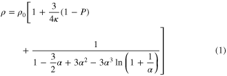


where ρ0 is the resistivity of the bulk material, and 12.3 μΩ·cm is the value for the SnAg alloy [29]; P is the fraction of electrons scattered specularly at the surface, which takes values between 0 and 1; d is the diameter of the wire; λ is the mean free path of the bulk material, and 5.366 nm is the value for the SnAg alloy [30]; R denotes the scattering coefficients at the grain boundary, which takes values between 0 and 1; D is the mean grain size. In our case, the diameter and mean grain size of each individual 1D SnAg solder is 100 nm and 20 nm, respectively, as determined by the above and below morphogical analyses. As far as we know, there is no report on the fraction of the P electrons and the scattering R coefficients of the SnAg alloy nanowires. Steinhögl et al [31] reported that the P and R of the electrodeposited copper nanowire is 0.2–0.6 and 0.5, respectively. If we assume that the P and R of the 1D SnAg nanosolder is 0.5 and 0.5, a value of 28.9 μΩ·cm was obtained for the resistivity of the 1D SnAg nanosolder. This value is higher than the above standardized bulk value of 12.3 μΩ·cm [29]. Two main reasons were deduced to have caused this difference. Firstly, a layer of 4–7 nm SnO2 oxide covers the outer surface of individual SnAg nanosolders, according to the detailed characterization of the 1D SnAg nanosolders below; this forms a metal-semiconductor contact and may cause fringing field effects on the electrical resistivity of the nanosolder. Secondly, there are at least three phases: β-Sn, Ag3Sn and SnO2 in a 1D SnAg nanosolder. Also, there are different grain sizes and crystallographic properties that may change from sample to sample. More detailed investigations of the electrical properties of 1D SnxAg1 − x nanosolders are ongoing and will be reported soon. Nevertheless, this result shows that the electrical property of the 1D SnAg is good enough to be used as a high-quality nanoscale solder. The detailed electrical testing method of the individual nanowires is described in our previous report [6, 25]. In addition, the current versus voltage behaviors of both the probes and the nanowire circuit are linear, as shown in figure 2(f), which indicates remarkably low-resistance ohmic contacts.
3.3. Nanowire chemical and crystal structural characterization
The chemistry of the 1D SnAg nanosolder was characterized in detail by EDX, XPS and STEM mapping on a 300 kV HRTEM. Figure 3(b) shows a representative EDX spectrum of three 1D SnAg nanosolders, which are shown in figure 3(a). The Sn and Ag peaks come from the 1D SnAg nanosolders. The O peak should originate from the 1D nanosolder, which is deduced to be due to the partial oxidization of the 1D SnAg nanosolders. The C and Mo peaks are believed to derive from the holey carbon-coated molybdenum grid, which was confirmed by the measurement of an EDX baseline of an empty holey carbon-coated molybdenum grid. A quantitative analysis of this spectrum reveals that the chemical composition of individual 1D SnAg nanosolders is a 96.5:3.5 weight ratio of Sn:Ag, which is the same as the standardized eutectic phase of bulk SnAg alloy [32].

Figure 3. Chemical analysis of the 1D Sn-3.5Ag nanosolders: (a) HAADF–STEM image of an investigated 1D Sn-3.5Ag nanosolder. The red square shows the scanning area of the elemental mapping; (b) the EDX spectrum acquired from the nanowire marked by a red square; (c) the EDX line-scan spectrums of Sn-K/L and Ag-K/L from the nanowire marked by the red line; (d)–(f) the EDX elemental mappings of O-K, Ag-L and Sn-L; (g) the XPS spectrums for Sn3d and Ag3d after Ar ion sputtering for 0, 50, 100, 150, 200, 300, 400, 500, 600 s, respectively. The colors represent various values: purple for 0 s, orange for 50 s, yellow for 100 s, turquoise for 200 s, fuchsia for 300 s, blue for 400 s, green for 500 s and red for 600 s; (h) the XPS depth quantification after Ar ion sputtering.
Download figure:
Standard image High-resolution imageThe chemical distributions of the 1D Sn-3.5Ag nanosolder were subsequently studied by an EDX elemental line-scan and a mapping analysis technique. Figure 3(c) shows the EDX line-scan spectra of Sn-Kα/Lα and Ag-Kα/Lα taken across the 1D nanosolder, acquired using a 3.5 μm scan line parallel to the nanowire axis (as marked by the red line in figure 3(a)) and a 1.5 nm beam spot-size. We determined that the intensities of Sn and Ag are stable in error and are equal along the wire axes, revealing a uniform chemical phase. In addition, the intensity of Sn is higher than that of Ag, revealing that the chemical content of Sn is higher than Ag. Figures 2(d)–(f) further show the EDX elemental mappings of Sn-Lα (3.44 keV), Ag-Lα (2.98 keV) and O-Kα (0.52 keV), respectively. The elements of Sn and Ag are nearly evenly distributed throughout the whole nanosolder, indicating a uniform Sn-3.5Ag chemical phase. The even distribution of the oxygen element reveals that individual 1D Sn-3.5Ag solders are slightly oxidized after they are released from the AAO or PC templates.
In order to accurately determine the chemical states, the as-grown 1D SnAg nanosolders were further examined by XPS while they were still embedded in situ in the PC templates by Ar ion beam sputtering. The templates were cross-sectioned in parallel to the 1D SnAg nanosolder length axes by sputtering away (layer by layer) the top surface of the PC template. Figure 3(g) shows the relevant XPS spectra of Ag 3d and Sn 3d after Ar ion beam sputtering for 0 s, 50 s, 100 s, 150 s, 200 s, 300 s, 400 s, 500 s and 600 s, respectively; the corresponding depth profile analysis is shown in figure 3(h). The binding energies were calibrated using the C 1 s peak of 284.6 eV as the standard. The SnAg alloy 3d spectrum has two peaks because the spin–orbit of the 3d state is coupled with a spin-orbital separation of 8.5 eV for Sn and 6.0 eV for Ag [33]. For simplicity, only Sn 3d5/2 and Ag 3d5/2 were studied. The published binding energy of SnAg 3d5/2 indicated that the peak, which was in the range of 484.5 eV−485.2 eV, is attributed to Sn, the range of 486.0 eV−486.8 eV is attributed to SnO, the range of 486.4 eV−486.9 eV is attributed to SnO2, the range of 368.1 eV−368.3 eV is attributed to Ag and the range of 367.3 eV−368.0 eV is attributed to Ag oxides [33]. One can see that the Ag 3d5/2 peaks at 368.3 eV bonding energy in figure 3(g) can be attributed to metallic Ag, and there is no peak shift before and after the Ar ion beam sputtering; this indicates a stability of the Ag chemical phase along with the nanowire length. The Sn 3d5/2 spectra consist of two peaks located at 484.3 eV and 486.4 eV, indicating a formation of metallic Sn and SnOx, respectively. A quantitative analysis of the Sn3d5/2 spectrum before the Ar ion beam sputtering (purple spectrum) reveals the area fractions of Sn and SnOx to be 24.8% and 74.2%. This result indicates that the top end of the 1D SnAg alloy solders, which were exposed to air, were partly oxidized. After Ar ion beam sputtering at 50 s, the peak of the Sn drastically increases, and a quantitative analysis indicates a 65.2:34.8 area ratio of Sn:SnOx. The proportion of the Sn metallic state continues to grow over the sputtering time. After the sputtering time increased beyond 500 s, the quantitative analysis of the XPS wide spectrum revealed that the 1D SnAg nanosolders reached a stable 96.54:3.46 mass ratio of Sn:Ag and the oxygen peak could not be detected. This result is the same as the above EDX measurement in error. Therefore, the chemical composition of the 1D SnAg nanosolders in this work is inferred to be Sn-3.5Ag.
Figure 4(a) shows a TEM image of two single 1D Sn-3.5Ag nanosolders, which were exposed to air for 1 day after they were dispersed on the holey carbon-coated copper grid. One can see that a 5–7 nm oxide layer is covered on the surface, which is due to be oxidized and is consistent with the above EDX measurement. Due to the similar binding energies of SnO and SnO2, it is impossible to experimentally distinguish them by XPS at this stage. However, it is known that the Gibbs free energy of formation for SnO2 (−515.8 kJ mol−1) is much lower than that of SnO (−251.9 kJ mol−1) [34], which indicates that SnO2 is more thermodynamically stable. Therefore, it is deduced that the observed tin oxide film covered on the outer surfaces of the two 1D SnAg nanosolders should be SnO2.

Figure 4. TEM structural analysis of the 1D Sn-3.5Ag nanosolders: (a) Two investigated 1D SnAg nanosolders covering a 4–7 nm oxide layer; (b) magnified view of the red square in (a); (c) SAED pattern of (b); (d)–(f) lattice images of the areas marked by the square 'D', 'E' and 'F' in (b), respectively; (g)–(i) CBED patterns of the area marked by the square 'D', 'E' and 'F' in (b), respectively. The insets of the relevant crystal models of the CBED patterns are included.
Download figure:
Standard image High-resolution imageThe crystalline structures of individual 1D Sn-3.5Ag nanosolders were characterized in detail using selected area electron diffraction (SAED), convergent beam electron diffraction (CBED) and high-resolution TEM (HRTEM). Figure 4(b) shows a magnified TEM image of the area marked by a red square in figure 4(a). Its corresponding SAED pattern is shown in figure 4(c), which reveals that the individual 1D Sn-3.5Ag nanosolder is a multi-crystal. In order to obtain clearer details of the crystalline phases in a 1D Sn-3.5Ag nanosolder, an HRTEM technique was employed. Figure 4(d)–(f) show lattice images of the areas marked by the square 'D', 'E' and 'F' in figure 4(b), respectively. The interplanar distances are measured as 2.37 Å and 2.67 Å for area D (figure 4(d)), which matches the (200) and (101) planes of tetragonal SnO2; as 2.61 Å for area E (figure 4(e)), which matches the (002) planes of orthorhombic Ag3Sn; and as 2.05 Å and 1.48 Å for area D (figure 4(d)), which matches the (−200) and (−112) planes of body-centered tetragonal (BCT) β-Sn.
To further verify the accuracy of the crystal measurements, CBED using a 0.5 nm spot size configuration was used to analyze these three detected areas. The corresponding CBED patterns of the 'D', 'E', and 'F' areas are shown in figures 4(g)–(i), which can be well indexed into the [010] crystallographic orientation of the tetragonal structure (inset of figure 4(g)), the [100] orientation of the orthorhombic structure (inset of figure 4(h)) and the [110] orientation of the body BCT structure (inset of figure 4(i)), respectively. These results are well matched with the HRTEM observations. We then concluded that the 1D Sn-3.5Ag nanosolder is comprised of matrix β-Sn and intermetallic compound Ag3Sn, which is similar with the crystal phases in a bulk Sn-3.5Ag [32].
3.4. Nanosolder reflow performance test
The melting point and melting behavior are the critical factors that determine the quality of a solder. In this work, we further investigated the melting point and melting behavior of the 1D Sn-3.5Ag nansolders. Figure 5(a) shows a representative DSC curve of 1D Sn-3.5Ag nansolders within the PC template, which was heated from 50 °C to 550 °C at 10 °C min−1; the inset displays the magnified view of the red region in figure 5(a). The curve trend rises due to the presence of the PC template. Also, three peaks can be seen that correspond to the three melting points 215.5 °C, 220.7 °C and 390.6 °C. With consideration to the above crystal phase analysis and the Sn-Ag phase diagram [32], these three peaks could be attributed as melting points of eutectic β-Sn plus Ag3Sn and monovariant Sn and Ag3Sn, respectively. Considering that the eutectic β-Sn plus Ag3Sn is the dominant phase in the individual 1D Sn-3.5Ag nanosolders, as detected by the above chemical and structure analyses, we concluded that the melting point of the 1D Sn-3.5Ag nanosolders is about 215.5 °C. This value is lower than the bulk Sn-3.5Ag solder of 221 °C [32], which indicates that the 1D Sn-3.5Ag nanosolders prepared in this work have good flow and wettability. This result confirms that the 1D Sn-3.5Ag nanosolders can be used as a high-performance nanoscale solder. The melting behavior of the tin oxide shell was not reflected in the curve due to the melting point of the SnO and SnO2, which are 1080 °C and 1630 °C, respectively. Therefore, it was deduced that the eutectic composition of the 1D Sn-3.5Ag naosolder should be shifted to the Sn rich corner, which is in agreement with the study of Sn-Ag nanoparticles [35, 36].

Figure 5. Melting behavior of the 1D Sn-3.5Ag nanosolders: (a) A representative DSC curve of Sn-3.5Ag solder nanowires in a PC template heated from 50 °C to 550 °C at 10 °C min. Inset: a magnified view of the red square; (b) SEM image of 1D Sn-3.5Ag nanosolders after preheating. Inset: a magnified view of the four nanosolders; (c) SEM image of 1D Sn-3.5Ag nanosolders after reflowing in the N2 environment under the usage of no-clean liquid flux. Inset: a magnified view of one sphere; (d) HAADF-STEM image of 1D Sn-3.5Ag nanosolders after reflowing; (e)–(i) EDX elemental mappings of O-K, Ag-K/L and Sn-K/L.
Download figure:
Standard image High-resolution image
To further understand the melting behavior of the 1D Sn-3.5Ag nanosolders, reflow experiments were carried out. Figure 5(b) shows a representative SEM image of a bundle of 1D Sn-3.5Ag nanosolders after preheating at 150 °C–180 °C. One can see that the nanowires nearly retain their original shapes but stick together more closely. The magnified image reveals the formation of a few protuberances along the naowire due to the movement of the molten Sn. Figure 5(c) is a representative SEM image of the 1D Sn-3.5Ag nanosolders after they were reflowed in the N2 atmosphere under the usage of no-clean liquid flux, which shows a dramatic morphological change from a wire shape to a spheroid shape due to the minimized surface energy at the liquid phase. The size of the reflowed Sn-Ag solders varied from hundreds of nanometers to several microns; this is is believed to be due to the random and nonuniform distribution of the nanowires and the merging of the liquid droplet. The inset of figure 5(c) shows a magnified view of one sphere, revealing that there is a translucent thin film covered on its surface.
The chemical distributions of the reflowed Sn-3.5Ag nanosolder were subsequently studied by the EDX elemental mapping technique using 300 kV HRTEM. Figure 5(d) shows a HADDF-STEM image of 1D Sn-3.5Ag nanosolders after complete reflowing; this image clearly reveals a cluster of spheres enclosed in translucent thin shells, as observed above. Figures 5(e)–(i) shows the corresponding EDX elemental mappings of oxygen, silver and tin. One can clearly see that oxygen exists on the whole structure, indicating that the surfaces of the reflowed solders have been oxidized; these solders may be formed during the cooling or storage process after reflowing. The Sn mappings (figures 5(i) and (h)) show a uniform distribution in each sphere. However, the Ag (figures 5(f) and (g)) appears segregated in the sphere. One can derive this result from the lower cooling rate (naturally cooled to room temperature), which prolongs the solidification period and thus makes Ag3Sn IMCs grow into a massive block [37].
4. Conclusion
In summary, we have demonstrated a fabrication method for 1D Sn-3.5Ag nanosolders. The practical application of welding nanopatterns at the nanoscale to test their quality as nanosolders reveals that 1D Sn-3.5Ag nanosolders can easily form remarkably reliable conductive joints, of which wettability, mechanical strength, controllability and reliability during the nanowelding process are proved to be much better than our previously reported Sn99Au1 and Au nanowires. The resistivity of the 1D Sn-3.5Ag nanosolder is measured to be 28.9 μΩ·cm, which should be in the first report. The XPS measurements confirm that the mass ratio of Sn:Ag is a stable 96.54:3.46. The EDX elemental mappings show that both the Sn and Ag elements are evenly distributed throughout the whole nanosolder. The reflow experiments reveal that the eutectic composition of the 1D Sn-Ag alloy nanowire is shifted to the Sn rich corner. We believe our work will contribute an important nanosolder for the future nanoindustry, which will be significant for the bottom-up localized assembly, integration, and repair of micro/nanodevices, nanoelectronics, nanosensors and nanoelectromechnical systems.
Acknowledgments
This work was supported by the National Basic Research Program of China (2012CB933104), the National Natural Science Foundation of China (11274145 and 11034004), the Program for Changjiang Scholars and Innovative Research Team in University (Grant No. IRT1251) and the Fundamental Research Funds for the Central Universities (lzujbky-2013-19, and 2022013zrct01).